and methodologies of automatic instruction set extension for configurable processors, recent study has shown that the limited data bandwidth available in the ...
Architecture and Compilation for Data Bandwidth Improvement in Configurable Embedded Processors Jason Cong, Guoling Han, Zhiru Zhang Computer Science Department University of California, Los Angeles, CA 90095
{cong, leohgl, zhiruz}@cs.ucla.edu
ABSTRACT Many commercially available embedded processors are capable of extending their base instruction set for a specific domain of applications. While steady progress has been made in the tools and methodologies of automatic instruction set extension for configurable processors, recent study has shown that the limited data bandwidth available in the core processor (e.g., the number of simultaneous accesses to the register file) becomes a serious performance bottleneck. In this paper we propose a new low-cost architectural extension and associated compilation techniques to address the data bandwidth problem. Specifically, we embed a single control bit in the instruction op-codes to selectively copy the execution results to a set of hash-mapped shadow registers in the write-back stage. This can efficiently reduce the communication overhead due to data transfers between the core processor and the custom logic. We also present a novel simultaneous global shadow register binding with a hash function generation algorithm to take full advantage of the extension. The application of our approach leads to a nearly-optimal performance speedup (within 2% of the ideal speedup).
1. INTRODUCTION Application-specific instruction-set processors (ASIPs) are a promising approach to combining the flexibility offered by a general-purpose processor and the speedup (and power savings) offered by an application-specific hardware accelerator. Generally, an ASIP has the capability to extend the instruction set of the base architecture with a set of application-specific instructions implemented by custom hardware resources. These hardware resources can be either runtime reconfigurable functional units, or pre-synthesized circuits. The recent emergence of many commercially available embedded processors with both configurability and extensibility (e.g., Altera Nios/NiosII [17], Tensilica Xtensa V/LX [18], Xilinx MicroBlaze [19], etc.) testifies to the benefit of this approach. A crucial step to achieving high performance in an ASIP design is to select an optimal custom instruction set. However, for large programs, this is a difficult task to manage by manual designs, and is further complicated by various micro-architectural constraints. This has motivated a large body of recent research to address the automatic instruction set extension problem. Most of the existing approaches attempt to discover the candidate extended instructions by identifying common patterns in the data flow graph of the given application, and then to select an appropriate subset of the candidate instructions to maximize performance under certain architectural constraints (e.g., the number of input and output operands, area constraints, etc.). Kastner et al. [12] proposes a simultaneous template generation
and matching method that constructs the candidate instruction set by clustering the nodes based on edge-type frequencies. Sun et al. [16] enumerates the possible extended instructions by repeatedly combining the smaller templates to form the larger templates. A comprehensive priority function is computed to rank and prune the candidate instructions. The method was recently extended by [6] to speed up the exploration process. Atasu et al. [4] imposes further constraints on the instruction topology and performs a branch-and-bound algorithm on a binary tree to determine whether or not to include a node into the candidate instruction. Although the existing techniques are efficient in identifying the promising candidate instructions, [11] points out that most of the speedup (about 60%) comes from the cluster with more than two input operands. This exceeds the number of read ports available on the register file of a typical embedded RISC processor core. Strictly following the two-input single-output constraint generally leads to small clusters with limited speedup. Generation of larger clusters with extra inputs is allowed in [16] by using the custom-defined state registers to store the additional operands. Unfortunately, at least one extra cycle is needed for each additional input to be loaded into a custom-defined state register. The communication overhead incurred because of these data transfers between the core processor and the custom logic can significantly offset the gain from forming a large cluster. A quantitative analysis of the data bandwidth limitation is given in [8], and the problem is directly addressed by augmenting the processor’s register file with an extra set of registers that are written transparently by the processor and used by the custom instructions. This avoids explicit move instructions from the core register file to the custom logic. Experiments show that a small number of shadow registers is sufficient to compensate a major portion of the performance degradation caused by the port number limitation. However, additional bits (two to three bits) need to be added in the instruction format, which is difficult to be encoded without increasing the instruction word length. A shadow register binding algorithm is also proposed as the associated compilation technique in [8]. This algorithm limits its scope within the basic block boundary. Our contributions in this paper are twofold. First, we propose a new low-cost architectural extension called hash-mapped shadow registers, which enables and significantly enhances the shadowregister-based scheme using a single control bit. Second, we present a simultaneous global shadow register binding with a hash function generation algorithm which fully exploits the benefits of shadow registers across the basic block boundaries. The remainder of the paper is structured as follows. We first present our architectural extension in Section 2. The algorithmic details for solving the global shadow register binding problem together with the hash function construction problem are
described in Section 3. Experimental results are shown in Section 4, followed by conclusions in Section 5.
very limited opportunities for compiler optimization to further improve performance.
2. ARCHITECTURE EXTENSION 2.1 Motivation
Shadow Registers with Multiple Control Bits: Shadow registers have been recently proposed [8] as an architectural extension to overcome the aforementioned limitations and difficulties. Figure 1 shows the block diagram of this architecture, in which the core register file is augmented by an extra set of shadow registers that are conditionally written by the processor in the write-back stage and used only by the custom logic.
However, such a scheme would restrict the custom instruction to having only two input operands, thus limiting the complexity of the computations. Generally, when the input number constraint is relaxed, higher performance speedup can be achieved by clustering more operations in one custom instruction to exploit more parallelism. Unfortunately, if a custom instruction needs extra operands, the processor core has to explicitly transfer the data from the register file to the local storage of the custom logic through the data bus, which may take multiple CPU cycles. This communication overhead will significantly offset the performance gain experienced by using the custom instruction.
2.2 Existing Solutions Several architectural approaches can be adopted to tackle the speedup degradation caused by the port number limitation. We shall discuss three existing approaches below. Multiport Register File: A straightforward method to increase data bandwidth for an instruction is the use of a multiport register file to introduce extra read ports. This allows the custom instruction to increase simultaneous accesses to the core register file. However, adding ports to the register file will have a dramatic impact on the energy and die area of the processor. As pointed out in [15], the area and power consumption of a register file grows cubically with its port number. Register File Replication: Register file replication is another technique used to increase data bandwidth. By creating a complete physical copy (or partial copy) of the core register file, the custom instructions can fetch the encoded operands from the original register file and the extra operands from the replicated register file. By using this approach, Chimaera [10] is capable of performing computations that use up to nine input registers. The reconfigurable logic is given direct read access to a subset of the registers in the processor by creating an extra register file which contains copies of those registers values, thus allowing complicated computations to be performed. Since the basic instructions cannot use the replicated register file, the complete register duplication approach will introduce considerable resource waste in terms of area and power. For the partial duplication approach, it enforces a one-to-one correspondence between a subset of registers in the core register file and those in the replicated register file, and the computation results are always copied to the replicated registers. This leaves
Core register file
Shadow registers
Data bus controller
Execution units
Processor core
Custom logic
The architectural model targeted in this paper is a classical singleissue pipelined RISC core processor, with a two-read-port and one-write-port register file. Under this processor model, a custom instruction follows the same instruction format and execution rules, which include: (1) The number of operands and results of a custom instruction are pre-determined by the base architecture; (2) The custom instruction cannot execute until the input operands are all ready; (3) The custom instruction can read the core register file only during the decode/execute stage, and can commit the result only during the write-back stage. This extensible architecture simplifies the implementation since the base instruction set architecture can be retained.
Figure 1. Shadow registers with multiple control bits. Any instruction (basic or extended) can either skip or copy the computation result into one of the shadow registers in the writeback stage. The copy/skip option and the address of the target shadow register need to be encoded as additional control bits in the instruction format. Table 1 shows one possible encoding for the extension with three shadow registers, in which two bits are needed. Table 1. An instruction encoding for three shadow registers. Operation Copy to shadow register Skip Instruction subword 00 01 10 11 Target shadow 0 1 2 Since the data is copied to the shadow registers transparently during the write-back stage, the communication overhead between the processor core and the custom logic can be greatly reduced. Moreover, under the above encoding scheme, each shadow register can be the physical copy of any register in the core register file, which creates a great amount of freedom and opportunities for the compiler optimization. Experiments in [8] have shown that a small number (typically less than four) of shadow registers is sufficient to compensate a major portion of the performance degradation caused by the port number limitation. However, additional bits (log2K+1 bits for K shadow registers) are required in the instruction format. Since the unused opcodes are usually limited in the common instruction format, it is not trivial to encode two or three extra bits without increasing the word length. In fact, we need to represent four distinct versions of one instruction to accommodate two extra control bits and eight versions for three bits, which is not practical in general.
2.3 Proposed Approach Shadow Registers with Single Control Bit Note that the shadow registers essentially act as a tiny cache located in the customer logic to temporarily store the recent computation results from the core processor. In this sense, the multiple-bit controlled shadow register set resembles a fully associative cache since each core register can be mapped to any entry of shadow register set. This full associativity requires the presence of multiple control bits in the instruction word to
identify the target shadow register. In this subsection, we propose to use a hash-mapped shadow register scheme to significantly reduce control bit overhead.
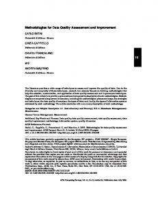
Hashing Unit
Shadow registers
Data bus controller
Core register file
Custom logic
Execution units
Processor core
Figure 2. Shadow registers with single control bit.
2.3.1 Hash-Mapped Shadow Registers Scheme Figure 2 shows the block diagram of our proposed enhancement. In this scheme, every instruction can also choose to either skip or copy the result into the shadow registers during the write-back stage. The key difference is that only the copy/skip option needs to be encoded as an additional control bit in the instruction format. The actual shadow register that will be written is determined by a pre-specified many-to-one hash function. Namely, the execution result to register R[i] in the core register file will be conditionally copied to register SR[j] in the shadow register set where j = hash(i). For example, one simple hashing scheme can be directed mapping where j = i mod K, assuming that we have K shadow registers. In general, the particular hash function can be performed by the hashing unit which resides in the custom logic using a fast and cheap lookup table, and reconfigured for different applications or different domains of applications.
2.3.2 Advantages and Limitations Since the shadow registers will be mainly used for storing the source operands of the custom instructions, the required number of shadow registers is generally much less than that of the core register file. Except for a small amount of extra interconnect and control logic introduced by the conditional copy path, the base datapath will remain the same. Therefore, the implementation tends to be very cost-efficient when compared to the prior approaches of using the multiport register file and register file replication. Note that the target shadow register address is determined by the hashing unit instead of being explicitly encoded in the instruction word. This allows more shadow registers (greater than three) without the penalty of increasing the number of control bits. More importantly, we believe that it is much easier to add (or encode) one single additional control bit without increasing the length of the instruction word. For example, in NiosII [17] R-type instructions there are several reserved bits that can be potentially used for advanced features. For the I-type and J-type instructions, there are 42 encodings specified for the 6-bit OP code field. This leaves more than 20 encodings unused, which are sufficient to accommodate the second versions of those particular instructions (e.g., arithmetic and load instructions) that can forward their results to the shadow registers. Clearly, our proposed single-bit controlled shadow register approach provides a much more viable solution compared to the original multi-control-bit shadow registers approach reviewed in Section 2.2.
One potential limitation of the hash-mapped shadow registers approach is that a predetermined many-to-one correspondence is enforced between the core registers and the shadow registers, which may restrict the opportunities for compiler optimization to further improve performance. However, we believe this limitation is minor because more shadow registers can be allocated to mitigate the problem. Essentially, we can trade off the associativity of the shadow register set for the number of entries.
3. SIMULTANEOUS GLOBAL SHADOW REGISTER BINDING WITH HASH FUNCTION GENERATION Shadow registers should be also considered during the compilation process to fully exploit the benefits of our proposed architectural extension. First of all, the compiler has to guarantee the integrity and the correctness of the program, e.g., it has to ensure that an active shadow register would not be overwritten during the execution of a custom instruction. Moreover, optimization techniques are needed to intelligently assign or bind the variables to the appropriate shadow registers. In [8], a shadow register binding problem was introduced as a special case of register allocation problem to maximize the usage of the shadow registers. Unfortunately, the proposed algorithm limits itself to a data flow graph only (i.e., within the basic block boundary). In this section we first present a global solution that performs shadow register binding across the whole control data flow graph using the predetermined hash function described below in subsection 3.1. We then show that the hash function generation can be carried out simultaneously with the shadow register binding in subsection 3.2.
3.1 Global Shadow Register Binding Under Prescribed Hash Function 3.1.1 Preliminaries Compiler optimization algorithms are usually performed on the control data flow graph (CDFG) derived from a program. On the top level of a CDFG, the control flow graph consists of a set of basic block nodes and control edges. Each basic block is a data flow graph (DFG) in which nodes represent basic computations (or instruction instances) and edges represent data dependencies. Throughout this section, we assume that given the profiling information, the ASIP compiler has generated extended instructions and mapped the application so that every node in the mapped CDFG corresponds to an instruction in the extended instruction set (including basic instructions and custom instructions). We also assume that each instruction produces at most one result, and the instruction scheduling and register allocation for the core registers have already been performed. Thus we know the shadow register to which an operand can be mapped with the given hash function. Our task is to appropriately assign the source operands of the custom instructions to the available shadow registers so that the potential communication overhead (in terms of the number of move operations) can be minimized. Specifically, the problem is solved in three steps: (i) We first perform a depth-first search to produce a linear order of all the instructions; (ii) Then we derive the live intervals for each shadow register candidate (i.e., data use); (iii) Based on the live intervals, we construct a compatibility graph and bind each shadow register independently.
3.1.2 Linear Ordering We adapt a linear scan register allocation technique to compute a global linear order of the instructions and derive the live intervals for the shadow register candidates in the CDFG. Linear scan register allocation was proposed by Poletto and Sarkar in [14]. It is a very simple and efficient algorithm that runs up to seven times faster than a fast graph coloring allocator and produces relatively high-quality code. We employ the depth-first method introduced in [1] to order the basic blocks. The final linear ordering is the reverse of the order in which we last visit the nodes in the preorder traversal of the graph. Figure 3 shows an example CDFG annotated with the linear numbering for each basic block. The complete sequence of basic blocks visited as we traverse the CDFG is 1, 2, 3, 4, 6, 7, 6, 4, 5, 4, 3, 2, 1. In this list, we mark the last occurrence of each number to get 1, 2, 3, 4, 6, 7, 6, 4, 5, 4, 3, 2, 1, which is the final ordering of the basic blocks. Additionally, the instructions inside one basic block are ordered according to the instruction scheduling. By combining these two numberings, we obtain a global sequence number (SN) for each instruction in the CDFG. In fact, the correctness of the algorithm does not depend on the ordering method. However, it may influence the quality of register binding. 1 51: r1 = …;
2
52: r2 = ext1 (…, r1, …); 31: v=…
53: r3 = ...v;
3
54: r4 = ext2 (…, r1, …); 55: r5 = ext3 (…, r3, …); 56: r6 = ext4 (…, r3, …);
4 6
62: v=…
53: …=v
78:…= v
5
7
Figure 3. A CDFG example with linear order.
3.1.3 Live Interval Generation Motivation As mentioned earlier, if the input number of a custom instructions exceeds the available read port count, extra data transfer (or move, for short) operations are needed to copy operands from the register file to the local storage in the custom logic. In our proposed architecture, if an operand is already in the shadow register, one move operation can be saved. 1
i1: r1 = …; i2: r2 = ext1 (…, r1, …);
2
i3: r3 = …v;
3
i4: r4= ext2 (…, r1, …);
4
i5: r5 = ext3 (…, r3, …);
5
i6: r6 = ext4 (…, r3, …); 6 (a)
(b)
Figure 4. An instruction sequence and its data flow graph. In addition, it is not necessarily optimal to keep a variable in the shadow register for its every use as pointed out in [8]. Figure 4
shows the data flow graph of the basic block 5 in Figure 3. Suppose the register file has only two read ports, and all the extended instructions have three input operands, then four move operations will be required without the shadow register. Assuming that there is one shadow register available, only two moves can be saved through the shadow register if we keep the variables in the shadow register for their entire lifetime. Interestingly, one more move can be saved if instruction i3 commits to the shadow register and overwrites the result of i1. Therefore, to achieve the maximum number of move operation saves, we should allow a value to be replaced in the middle of its lifetime. This motivates us to define the life intervals with respect to each data use of a variable instead of the variable itself.
Definition of Live Intervals To derive the live interval of a data use r, we need to consider the following three cases: (1) If variable r is defined (or assigned) within the same basic block of the subject use, and the definition is before the use, then the live interval is [s, t] where the SN of the definition instruction is s and the SN of the use instruction is t; (2) If all the definitions of variable r locate in the preceding basic blocks (precedence relationship is defined in terms of the linear order), then the live interval is [min(si), t] where min(si) denotes the SN of the definition instruction with the smallest numbering in the linear order; (3) If variable r has one definition after the subject use, it implies that r is assigned and used in a loop. In this case, we need to traverse the loop once, extending the live interval to [i*, j*] where i* and j* denote the smallest and largest SNs of any instructions in this loop. For the example in Figure 3, the use v at basic block 7 has two definitions in basic blocks 3 and 6, respectively. The live interval for use v is [31, 78]. We should notice that the life interval is a conservative approximation. Some subranges within [i, j] where variables are not live may also be included and are underutilized. However, the correctness of the program is not affected.
3.1.4 Binding for One Shadow Register The binding problem for one shadow register can be formulated as follows: One-shadow-register binding problem: Given a shadow register sr, a hash function h, and an interval set S in which each interval will be hash-mapped to sr, select a subset of non-overlapping live intervals in S and bind them to sr so that the maximum number of move operations can be saved. To accurately calculate the move reduction, a weighted compatibility graph G(V’, E’) can be built in the following way. Different from the conventional compatibility graph, each vertex v corresponds to an interval in S. We create an edge from v (with interval [i, j]) to v’ (with interval [i’, j’]) if and only if j