INSTITUTE OF PHYSICS PUBLISHING
NANOTECHNOLOGY
Nanotechnology 16 (2005) 913–917
doi:10.1088/0957-4484/16/6/048
Arrays of vertically aligned and hexagonally arranged ZnO nanowires: a new template-directed approach Hong Jin Fan1,3, Woo Lee1 , Roland Scholz1 , Armin Dadgar2 , Alois Krost2 , Kornelius Nielsch1 and Margit Zacharias1 1
Max Planck Institute of Microstructure Physics, Weinberg 2, 06120 Halle, Germany Institute of Experimental Physics, Otto-von-Guericke University, 39016 Magdeburg, Germany 2
E-mail:
[email protected]
Received 9 November 2004, in final form 18 March 2005 Published 19 April 2005 Online at stacks.iop.org/Nano/16/913 Abstract A new template-directed method for large-scale fabrication of hexagonally patterned and vertically aligned ZnO nanowires is demonstrated. The process involves a novel type of metal membrane, gold catalyst templates produced using the membrane as the deposition mask, and catalyst-guided vapour-phase growth of ZnO nanowires. The metal membranes, composed of hexagonal nanotube arrays, are electrochemically replicated from ordered porous alumina. The obtained ZnO nanowires are uniformly aligned perpendicular to the GaN surface and have a distribution according to the pattern defined by the nanotube membrane. We also demonstrate that by modifying the electrochemical parameters and growth conditions, the diameter of the nanowires can be varied in the range 30–110 nm.
1. Introduction ZnO-based one-dimensional (1D) nanoscale materials, as important functional oxide nanostructures, have received increasing attention over the past few years due to their potential applications in optoelectronic switches, highefficiency photonic devices, near-UV lasers, and for assembling complex three-dimensional nanoscale systems [1]. Most of these applications can be advanced if the alignment, distribution and aspect ratio of the 1D nanostructures can be controlled during the growth process. A straightforward approach for this purpose is to create patterned metal nanoparticles, which are used as catalyst templates for the subsequent guided vapour–liquid–solid (VLS) growth of nanowires [2]. In the past few years, a number of approaches have been used to obtain microscale-and nanoscale-patterned metal catalysts for successful large-scale fabrication of nanowires arrays. These microscale catalytic gold patternings were generated by the evaporation of gold through masks such as transmission electron microscopy (TEM) grids [3, 4] 3 Author to whom any correspondence should be addressed.
0957-4484/05/060913+05$30.00 © 2005 IOP Publishing Ltd
and monolayers of sub-micrometre spheres [5]. The gold pattern generated by the latter method was interconnected dots of several hundred nanometres in diameter. Therefore, the obtained nanowires were not totally separated from each other. For truly nanoscale patternings, the electron beam lithography (EBL) technique has been demonstrated for the fabrication of nanowire arrays of InP [6] and ZnO [7]. However, EBL is known as a relatively complicated and costly method, and is thus unsuitable for large-scale fabrication. Nanoimprint lithography (NIL) has also been used in Samuelson’s group to obtain highly ordered and spatially separated metal catalyst dots for subsequent growth of InP nanowire arrays [8]. NIL tends to be more promising for industrial usage as it is in many respects capable of producing structures comparable to those of EBL, but at a considerably lower cost and with a much higher throughput [8]. Recently, Greyson and co-workers [9] reported a soft-photolithographic etching route to obtain gold dot (40– 200 nm in diameter) patterns. The advantage of their method is that the gold dots can be patterned in a large scale (∼1 cm2 ) with variable symmetry (square, hexagonal and rectangular) and spacings. However, the grown nanowires are not straight or uniformly oriented, and several (up to 20) wires grow from
Printed in the UK
913
H J Fan et al
one defined catalyst spot. These drawbacks may hinder the nanowire arrays from device application considerations. In the present paper, a new template method for the fabrication of perfectly arranged arrays of ZnO nanowires is demonstrated. The catalyst gold nanodot templates are produced using a novel type of gold nanotube membrane (GNM) as a deposition mask. Our fabrication method is an inexpensive and generic approach and it is in principle applicable for the fabrication of any semiconductor nanowires on corresponding lattice-matched substrates. Hence, it reinforces the feasibility of creating nanoscale-patterned 1D nanomaterials for applications such as sensor arrays, field electron emitter arrays, and vertical field-effect transistors [7]. For the particular case of the present work on ZnO nanowires, we use highly doped GaN epilayers as substrates. GaN and ZnO have a similar fundamental bandgap energy (∼3.4 eV), the same wurtzite crystal symmetry, and a low misfit of the lattice constant (1.9%). This makes GaN a good candidate for both epitaxial growth [4, 10] and device applications of ZnO nanowires.
2. Experimental details 2.1. Fabrication of gold nanotube membranes First, monodomain anodic aluminium oxide (AAO) membranes were prepared by anodization of nanoindented aluminium foil as described previously [11]. Afterwards, a 3 nm gold film was plasma sputtered onto the AAO template surface, forming a thin conducting layer on the top part of the inner surface of the nanochannel as well as on the top surface of the AAO template. Further electrochemical deposition of gold at a current density of 1.5 mA cm−2 homogeneously thickens the conducting gold layer, resulting in a tubular gold nanostructure inside the alumina channels. Subsequently, the samples were transferred to a 30 wt% H3 PO4 etching solution to remove the alumina template. The released gold nanotube membrane remained floating on the surface of the solution. Then the etching solution was deionized by adding water. Fabrication of GNMs with different tube diameters (Dtube , in the range from sub50 nm to 230 nm) can be realized by using AAO templates with different pore diameters and adjusting the electrochemical deposition time. More details on the GNM will be reported elsewhere [12]. 2.2. Preparation of arrays of gold dots The GNMs floating on the surface of the deionized solution were transferred onto the substrate surface by immersing the substrate into the solution and lifting up the substrate together with the GNM. Thermal evaporation of gold is conducted in a high vacuum chamber during which the deposited film thickness was monitored in situ. A nominal thickness of 2–3 nm was used in our experiments. Subsequently, the GNMs were carefully removed using an adhesive tape, leaving the arrays of gold nanodots on the substrate surface. 2.3. Growth of ZnO nanowire arrays The substrates used are 500 nm thick GaN(0001) layers epigrown on Si(111) by metal organic chemical vapour 914
deposition [13]. Synthesis of ZnO nanowires was conducted via vapour deposition in a double tube system. A similar setup has been independently adopted by Geng and co-workers [14] in their growth of aligned ZnO nanowires on Si substrates. A mixture of ZnO and graphite powder (1:1) was put inside a small alumina tube (1.5 cm inner diameter and 10 cm length) at its closed end, and the gold-coated substrates at the other open end with about 8 cm distance in between. The whole system was transferred into a large quartz tube (5 cm inner diameter and 20 cm length) with the source being at the centre and the substrate downstream near the end of the heating zone. The tube was heated up by a resistance furnace to 920–950 ◦ C and kept there for 20 min. Due to a temperature gradient, the substrate temperature was correspondingly 730–810 ◦ C, as measured by a thermocouple. The residual and/or leaky O2 , with a partial pressure ∼10−4 mbar, in our standard setup provides the oxygen source for the oxidation of Zn. After the reaction, the furnace was switched off and cooled slowly down to room temperature. During the whole process, the tube pressure was maintained at 200 mbar by a constant flow of pure Ar gas (25 sccm). Scanning electron microscopy (SEM) images were acquired using a JEOL JSM-6300F (operating at 10 kV). Highresolution TEM images and diffraction patterns were obtained on a JEOL JEM-4010 (operating at 400 kV).
3. Results and discussion The whole fabrication process involves three main steps, as is schematically demonstrated in figure 1. First, GNMs comprising hexagonally arranged nanotubes were electrochemically fabricated by replicating the master structure of porous AAO. Subsequently, gold nanodot arrays were produced by thermal evaporation of gold using the GNMs as shadow masks. Finally, ZnO nanowires were grown on GaN(0001)/Si(111) layers directed by the catalytic gold nanodots. Details of each step are described in the experimental section. 3.1. Pattern of catalytic gold nanodots Free-standing GNMs were replicated from monodomain AAO membranes through an electrochemical process (see section 2.1). Figure 2(a) presents a low-magnification top view of the backside of a thus obtained GNM. A perfect hexagonal arrangement and uniform alignment of the nanotubes is achieved on a large scale, mirroring the initial monodomain pore arrays of the master AAO template. In fact, the overall size of GNMs can be as large as some square centimetres, as defined by the large AAO template. The inset in figure 2(a) shows an enlarged view of the front side of a tube array whose inner diameter is around 130 nm with an inter-tube distance of 500 nm. The bird’s-eye view of the membrane (figure 2(b)) clearly illustrates the highly ordered alignment of the monosized nanotubes. Using the GNMs as shadow masks, arrays of catalytic gold nanodots were obtained through a simple thermal evaporation process followed by removal of the masks. Figure 2(c) shows the gold dot arrays with the same hexagonal pattern as the mask. When a GNM with Dtube = 130 nm was used, the
Arrays of vertically aligned and hexagonally arranged ZnO nanowires
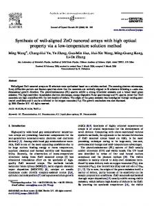
a)
AAO membrane
Au mask
a)
500 nm
Au mask
b) GaN/Si substrate
7 µm
Au dots b)
ZnO nanowires
c)
Figure 1. Schematics of the fabrication process of homogeneous arranged ZnO nanowire arrays. (a) A gold nanotube membrane is electrochemically replicated from the monodomain porous aluminium oxide. (b) The gold nanodot array is thermally evaporated using the gold nanotube membrane as a shadow mask. (c) Vapour transport and deposition growth of ZnO nanowires using the gold nanodots as catalyst. Through this fabrication process, the initial monodomain hexagonal pattern of the aluminium oxide is preserved. (This figure is in colour only in the electronic version)
printed gold nanodots have a mean size of 100 nm and an inter-dot separation of about 500 nm (figure 2(c)). In order to prepare arrays of smaller gold nanodots, membranes with reduced tube diameters (Dtube ≈ 60 nm) were fabricated by adjusting the electrochemical deposition parameters to thicken the wall of the nanotubes. It is worth noting that such noble nanotube membranes are advantageous over AAO membranes in their applications as shadow masks. Due to the stiffness and the hydrophilicity, AAO membranes allow only inhomogeneous pattern transfer. Voids of mm2 areas usually occur, although µm2 areas of ordered arrays are basically possible. In contrast, the GNMs are flexible, easy to handle, and additionally the gold surface can be easily functionalized. This assures a high accuracy of the pattern transfer. In our experiment, the smallest pore diameter of the AAO template applicable for the eventual growth of nanowire arrays is about 90 nm. In addition, although the mask could be reused for multiple depositions, the deposited Au dots would become smaller and smaller and the arrays become incomplete as some nanotubes would be clogged up. In our experiments, all the GNM masks used are freshly fabricated.
2 µm c)
2 µm Figure 2. (a) SEM image of a gold nanotube membrane viewed from the front side. Inset: enlarged top view. The inner diameter of the nanotube is about 130 nm. (b) Inclined view of the gold nanotube membrane showing the perfect alignment of the nanotubes. (c) Gold dot arrays obtained by thermal evaporation using the gold membrane as a shadow mask followed by removal of the membrane.
3.2. Periodic arrays of ZnO nanowire Growth of ZnO nanowires were conducted via vapour deposition in a double tube system by carbothermal reduction of ZnO powder. The relatively low temperature at the substrate position, due to the existence of temperature gradient, was effective to minimize the thermally induced movement of nanosized liquid gold, thus preserving the initial nanodot gold pattern. It should be mentioned that the use of a small tube 915
H J Fan et al
wire axis [0001]
0001
1120
[1010]
2 nm Figure 4. HRTEM lattice image recorded from a segment of an individual nanowire. Inset: corresponding electron diffraction pattern.
Figure 3. A general view of the ZnO nanowire arrays. (a) Top view, (b) inclined view. (c)–(d) The corresponding high-magnification views. Scale bars: 1 µm.
is essential in our experiments for successful fabrication of periodic nanowire arrays. A high Zn vapour pressure is created at the open end of the small tube where the substrates are located, which assures a sufficient vapour supersaturation of Zn and thus an increased growth rate for the ZnO nanowires. Growth at a temperature >800 ◦ C for a prolonged time usually results in a continuous layer or network of ZnO, in addition to nanowires or short rods. The SEM images in figure 3 present a general view of the ZnO nanowire arrays obtained by using the gold template in figure 2(c). It is clear from figures 3(a) and (b) that the nanowires are arranged in a periodic hexagonal pattern in a large scale, which preserves the initial gold pattern after the growth process. The high-magnification images in figures 3(c), (d) reveal that the nanowires have hexagonal ends, indicating that their main axis is oriented along [0001]. The wires are oriented perpendicular to the substrate surface. This is a result of the epitaxial growth of ZnO at the (0001) GaN surface [4]. The interwire distance is constant at 500 nm, as predefined by the hole-to-hole distance of the membrane mask. 916
The average height of the wires after a growth time of 20 min is 1.5 µm. A pyramidal film was noted at the base of the wires. This appears to be a typical phenomenon in the vapourphase epitaxial growth of nanowires [5, 15]. In our case, the film is determined to be ZnO by TEM investigations. The film forms in an early stage and serves as nucleation sites for subsequent growth of vertical nanowires, in a way similar to the self-organization process we reported previously [16]. The crystallographic orientation of the nanowires was determined using TEM. From the high-resolution TEM image recorded from a segment of an individual nanowire (figure 4), the distance between the parallel planes along the wire axis corresponds to a d-spacing of the (0001)-planes of 0.52 nm. The selected area electron diffraction confirms that the nanowires are wurtzite single crystals with the main axis along the [0001] direction. The above template-directed approach also allows an alteration of the diameter of the nanowires. By changing the electrochemical deposition parameters, a GNM with reduced tube size can be easily fabricated. By using these small Dtube masks for gold deposition, as well as under adjusted growth conditions (see the following), small diameter nanowires can be fabricated. Figure 5 illustrates an example of the size variations. The mean values of Dtube of the deposition mask shown in figures 5(a) and (c) are 130 and 60 nm, respectively. Figures 5(b) and (d) show the corresponding ZnO nanowires obtained. The mean values of the nanowire diameters are 85 nm for figure 5(b) and 50 nm for figure 5(d). Note that some spots in the hexagonal pattern are missing in figure 5(d). This is because some holes in the 60 nm membrane are nearly closed at their ends (see figure 5(c)), which blocks the gold vapour atoms during the thermal evaporation process. Nevertheless we believe that this can be improved if other Au deposition methods are used, for example, pulsed laser deposition. It is worth mentioning that, while growth of thin nanowires needs small catalytic gold, i.e., a deposition mask with reduced Dtube , the wire diameter is also strongly dependent on temperature. From repeated experiments with different temperatures and GNMs, we found a range of temperatures correspond to a given Dtube . In order to grow a single wire at the 110 nm gold nanodot site (corresponding to Dtube = 130 nm), a source temperature of about 935–950 ◦ C (growth temperature ≈ 800 ◦ C) is necessary (see figure 5(b)). However, for the growth of sub-70 nm nanowires at the catalytic sites obtained from the Dtube = 60 nm mask, the source temperature should be kept below 930 ◦ C (growth temperature ≈ 730 ◦ C;
Arrays of vertically aligned and hexagonally arranged ZnO nanowires
Figure 5. Size variation of the nanowires. Top view of the gold nanotube membranes with inner tube diameters of (a) ≈130 nm and (c) ≈60 nm. (b), (d) ZnO nanowire arrays with a mean diameter of 95 and 50 nm by using the shadow masks in (a) and (c), respectively. The source temperatures were set at 950 ◦ C in (b) and 920 ◦ C in (d). Scale bars: 500 nm. Note that some spots in the hexagonal pattern are missing as can be seen in (d). This is because of the small diameter of the nanotubes, which blocks the gold vapour atoms during the thermal evaporation process.
see figure 5(d)). Such a temperature effect is also demonstrated in figure 6, in which a gold array obtained from a Dtube = 130 nm mask was used at a source temperature of 920 ◦ C. As seen, 2–3 nanowires, ≈40 nm in diameter, grow from a single gold site. This is a consequence of the splitting of original Au pads into tiny particles (see the inset in figure 6), so that each tiny particle itself guides the growth of one thin ZnO nanowire [4]. Based on the above results, there seems to be a delicate balance between the gold dot size and temperature and/or vapour pressure, in order to realize only one wire from one gold dot. A possible reason is that Au nanodroplets in a certain size range are thermodynamically more favourable than others during the nucleation and growth process under specific conditions (e.g., vapour supersaturation) [2, 17]. However, our fabrication approach also possesses drawbacks. First, the spacing of the ZnO nanowire arrays is not adjustable because of the fixed lattice constant and symmetry of the initial AAO template. This might be overcome by combining the nanoindentation and self-organization process of porous alumina [18], so that GNMs with reduced lattice constants can be obtained. Second, our nanowires have a relatively broad size distribution (see figure 5) despite the homogeneity of the deposition mask. Improvement of the growth conditions, e.g., sampling geometry, is necessary, and work on this is in progress.
4. Conclusion We have demonstrated a new template method for reproducible fabrication of hexagonally patterned and vertically aligned ZnO nanowires on conducting GaN layers. The gold catalyst nanodot templates were produced using a novel type of metal nanotube membrane as the deposition mask. The obtained ZnO nanowire array has the same hexagonal pattern as that
Figure 6. ZnO multiple nanowire arrays obtained using the shadow mask with Dtube = 130 nm but at a source temperature of 920 ◦ C. Inset: result of annealing the catalytic Au template under the same condition except that there is no ZnO and carbon source. The initial Au pads split into tiny particles.
of the initial membrane. By choosing different-sized masks and suitable growth conditions, the diameter of the ZnO nanowires can be varied from 30 to 110 nm. Such vertically aligned ZnO nanowire arrays may have potential applications as nanoactuators and piezoelectric transducers. More importantly, our technique could be extended to the fabrication of other one-dimensional semiconductor nanostructures (e.g., Si, Ge, GaN).
References [1] Xia Y, Yang P, Sun Y, Wu Y, Mayers B, Gates B, Yin Y, Kim F and Yan H 2003 Adv. Mater. 15 353 [2] Wagner R S and Ellis W C 1965 Trans. Metal. Soc. AIME 233 1053 [3] Yang P, Yan H, Mao S, Russo R, Johnson J, Saykally R, Morris N, Pham J, He R and Choi H J 2002 Adv. Funct. Mater. 12 323 [4] Fan H J, Fleischer F, Lee W, Nielsch K, Scholz R, Zacharias M, G¨osele U, Dadgar A and Krost A 2004 Superlatt. Microstruct. 36 95 [5] Wang X, Summers C J and Wang Z L 2004 Nano Lett. 4 423 [6] Martensson T, Borgstrom M, Seifert W, Ohlsson B J and Samuelson L 2003 Nanotechnology 14 1255 [7] Ng H T, Han J, Yamada T, Nguyen P, Chen Y P and Meyyappan M 2004 Nano Lett. 4 1247 [8] Martensson T, Carlberg P, Borgstrom M, Montelius L, Seifert W and Samuelson L 2004 Nano Lett. 4 699 [9] Greyson E C, Babayan Y and Odom T W 2004 Adv. Mater. 16 1348 [10] Park W I and Yi G C 2004 Adv. Mater. 16 87 [11] Choi J, Chilling J, Nielsch K, Hillebrand R, Reiche M, Wehrspohn R B and G¨osele U 2002 Mater. Res. Soc. Symp. Proc. 722 L5.2.1 [12] Lee W, Alexe M, Nielsch K and G¨osele U 2005 Chem. Mater. submitted [13] Dadgar A et al 2003 Phys. Status Solidi c 0 1583 [14] Geng C, Jiang Y, Yao Y, Meng X, Zapien J A, Lee C S, Lifshitz Y and Lee S T 2004 Adv. Funct. Mater. 14 589 [15] Nguyen P, Ng H T, Yamada T, Smith M K, Li J, Han J and Meyyappan M 2004 Nano Lett. 4 651 [16] Fan H J, Bertram F, Dadgar A, Christen J, Krost A and Zacharias M 2004 Nanotechnology 15 1401 [17] Givargizov E I 1975 J. Cryst. Growth 31 20 [18] Choi J, Nielsch K, Reiche M, Wehrspohn R B and G¨osele U 2003 J. Vac. Sci. Technol. B 21 763
917