Based on overload tests of our analog nanovoltmeter, the input stage typically ... 2. Cryocooled programmable Josephson voltage standard. Two nominally identical .... A polarity set consists of 15 DVM readings at 10 power line cycles each.
Automated Direct Comparison of Two Cryocooled 10 Volt Programmable Josephson Voltage Standards
Alain Rüfenacht1, Yi-hua Tang2, Stéphane Solve3, Anna E. Fox1, Paul D. Dresselhaus1, Charles J. Burroughs1, Robert E. Schwall1, Régis Chayramy3, and Samuel P. Benz1 1
National Institute of Standards and Technology, NIST, Boulder, CO 80305, USA National Institute of Standards and Technology, NIST, Gaithersburg, MD 20899, USA 3 Bureau International des Poids et Mesures, BIPM, Pavillon de Breteuil, 92312 Sèvres Cedex, France 2
ABSTRACT We have performed direct dc comparisons between two cryocooled 10 V programmable Josephson voltage standards utilizing an automated synchronization scheme for the voltage reversals, which enables the use of a high-sensitivity analog null detector on its 10 µV range. No switches or manual operations are necessary to protect the null detector from overload signals. The agreement measured between the two voltage standards at 10 V is 9 parts in 1012 with a relative combined uncertainty of 29 pV/V (k=2). Since both systems can be operated floating from Earth potential, various grounding configuration of the measurement circuit were investigated, allowing evaluation of the comparison result on various leakage current paths to ground. Comparing the two systems under various grounding conditions enables minimization of the leakage current errors, optimization of the system performance by revealing leakagelimiting components, and verification of key elements of the uncertainty budget for the measurement method.1
Index Terms — Digital-analog conversion, Josephson arrays, standards, superconducting integrated circuits, voltage measurement.
1
Contribution of the U.S. government, not subject to copyright.
Page 1 of 25
1. Introduction The National Institute of Standards and Technology (NIST) programmable Josephson voltage standard (PJVS) [1] with an output voltage of 10 V has recently been fully implemented on a cryocooler [2]. Turnkey cryocooled PJVS systems are replacing conventional Josephson voltage standards, not only in national metrology institutes (NMIs), but also in primary calibration laboratories (PCLs). Combining intrinsic stability and larger immunity to external noise, PJVS systems offers a larger palette of applications beyond the calibration of secondary voltage standards, including accurate voltage references in electronic kilogram experiments (Kibble balances and Joule balances) [3-6], and lowfrequency stepwise-approximated waveforms for electric power standards [7-8]. With the forthcoming redefinition of the SI [9], PJVS systems will become a direct realization of the unit volt. Consequently, direct PJVS to PJVS comparisons [10] are becoming prevalent, not only to support the NMIs calibration and measurements capabilities (CMCs) within key comparisons of the Consultative Committee for Electricity and Magnetism of the Bureau International des Poids et Mesures, but also to qualify the performance of PJVS systems disseminated to the PCLs. The lowest Type-A uncertainty in direct voltage standard comparisons is generally achieved with the use of an analog null detector [10-11]. However, use of an analog detector often demands fastidious manual operations to prevent overloading during PJVS polarity reversals, which are required to eliminate the contributions of thermal electromotive forces. Based on overload tests of our analog nanovoltmeter, the input stage typically takes several minutes to completely recover. This paper presents results of the first fully automated direct comparison of two cryocooled 10 V PJVS systems. We have developed a synchronization method to switch simultaneously the polarity of both Josephson arrays without overloading the input stage of the analog null detector. The main advantage of this method is the ability to automatically acquire larger data sets, thus improving the statistical uncertainty of the comparison and eliminating the risk of incorrect manual operation causing accidental overloads. To ensure the quantum locking range of the quantized voltages, all comparison measurements were performed with an offset current applied to both Josephson arrays. Analysis of the results when grounding one node of the measurement circuit versus leaving both arrays floating is presented. Various grounding configurations of the measurement circuit were investigated and found to influence the leakage current path. Finally, since the leakage current is often the largest source of voltage error in direct JVS comparisons, we present a summary of the best practices for grounding the Josephson arrays that minimize leakage current errors.
Page 2 of 25
2. Cryocooled programmable Josephson voltage standard Two nominally identical cryocooled PJVS systems were used for this direct comparison. These systems were identified as PJVS(1) and PJVS(2). Each PJVS was equipped with the same instruments for biasing and cooling the Josephson junction arrays, including dc current sources, microwave sources, temperature controllers, cryostats, and Gifford-McMahon cryocoolers. Details about the 24-channel dc current bias sources can be found in Ref. [12]. The cooling power available with each system at a temperature of 4 K was about 200 mW [2]. Unlike the PJVS systems cooled with liquid helium, which require manual cooldown and warm-up of the arrays and manual connection and disconnection of the bias leads, the cryocooled PJVS is a true turnkey system which includes self-checks of the bias current operating margins for all 23 sub-arrays, self-diagnostics, and automated optimization of the microwave bias and operating temperature. Each 10 V PJVS array contains more than a quarter million Nb/NbxSi1x/Ni Josephson junctions (JJs) [13]. The device packaging for the 10 V arrays was designed to provide back-side cooling when mounted on the cryocooler [14], but is also compatible with the 2.57 cm diameter clearance of our standard liquid helium dip probe shield can. The device packaging is fitted with a 30-pin cryogenic-compatible connector to provide the bias current to the selected 23 sub-arrays [15]. This feature enables testing of the device in liquid helium before mounting the package on the cold head of a cryocooler. The dc bias current distribution within the array, the coldhead temperature (T), and the selected microwave bias frequency (fCW) and bias power were different for each system and array because the system automatically optimizes all bias parameters and operating temperature for each chip operated in the PJVS system [2]. The number of junctions for each subarray of both PJVS systems are reported in Table 1. •
•
The PJVS(1) array, operated at T = 4.25 K and fCW = 20 GHz, has a quantum locking range (formerly described as flat-spot [12]) of 0.94 mA when all subarrays, except #12, are biased in series and opposition (0 V across the entire device). The PJVS(2) array, operated at T = 4.1 K and fCW = 18.38 GHz, has a quantum locking range of 1.45 mA when all subarrays are biased in series and opposition (0 V across the entire device).
Each PJVS uses a different total number of junctions, bias frequency, and dc bias configuration to produce comparable output voltages. The microwave frequency of each PJVS is precisely tuned to the same 10 V output voltage to within 0.1 nV by adjusting the microwave frequency of each system using the 12 digits of resolution provided by the microwave synthesizer. The frequencies were set to fCWPJVS(1)= 19.999 913 151 365 GHz and fCWPJVS(2)= 18.379 925 659 035 GHz. The current bias polarities distributed to the sub-arrays of PJVS(1) and PJVS(2) are shown respectively in columns 3 and 6 of Table 1. Prior to performing the comparison measurements, the leakage currents of both systems were individually evaluated with the method described by Solve [10]. The leakage currents to Earth ground (LCG) reported in Table 2 was extracted from the measurement of the voltage drop across a 2 kΩ resistor connected between the PJVS array and Earth ground, and with the PJVS array producing a voltage of 10 V. Significant differences in the LCG depend on whether the resistor is connected to the low or high side of the PJVS arrays (DAC 0 or 23, respectively). However, the LCG values measured for Page 3 of 25
both PJVS systems are similar. The determination of LCG is highly sensitive to external perturbations (electrostatic fields, microphonic noise); the relative accuracy of the value reported is of the order of 5 %. The last column of Table 2 reports the equivalent leakage resistance (RL), calculated from the leakage current measurements at 10 V. 3. COMPARISON MEASUREMENT SETUP AND SYNCHRONIZATION The comparison measurement setup is presented in Fig. 1. An analog nanovoltmeter (NVM), EM N11 2, was used as a null detector to measure the voltage difference between the two cryocooled voltage standards, PJVS(1) and PJVS(2). Analog nanovoltmeters can provide a factor of 2 improvement in the measurement noise compared to that of the best digital null detectors [16, 17]. Analog null detectors are routinely used by BIPM in option A of the protocol of BIPM.EM-K10 key comparison framework [18]. Another type of NVM [19] has also been developed for such application, but it was not evaluated in this study. If the input stage of the NVM is overloaded, then the recovery time is related to the magnitude of the overload voltage and overload duration. To avoid overloads, all previously reported NVM voltage standard comparisons had been manually performed [10] and a protection circuit was required at the input to the NVM that was engaged at each PJVS polarity reversal. We avoid overloads with an innovative approach that simultaneously reverses the polarity of both PJVS arrays, such that the magnitude of the voltage at the NVM input remains within the selected 10 µV range. Our NVM measurements are fully automated without any manual intervention, allowing acquisition of large data sets and removal of potential errors in manual operation. Each synchronous change of voltage uses a four-step waveform (Table 3) triggered by four successive clock pulses at 5 kHz3 (Fig. 2). In fact, a twostep waveform would be adequate, but since the 24-channel current source implemented with our PJVS requires at least 4 steps in memory to run a waveform, the waveform used is twice repeated (step #1 = step #2 and step #3 = step #4). The waveform is loaded in the memory of both current sources and is programmed to run for a single cycle. Once the first cycle is completed, the PJVS voltage remains at the last voltage of the waveform. The microwave frequency of both PJVS circuits is adjusted prior to the start of the waveform (when the arrays are at 0 V). This waveform synchronization method can also be modified to generate a more gradual voltage ramp. However, since the two arrays (Table 1) have different fCW, one cannot guarantee that the differential voltage at every incremental step of the ramp will remain within the range of the NVM. Such a ramp may also be difficult to implement when comparing two PJVS systems of different type [11, 20-28]. The waveform presented in Fig. 2, has only two voltages, and can be generalized for the comparison of different types of PJVS arrays. We tested the overload recovery of our NVM by deliberately delaying the clock pulse sent to PJVS(2) relative to the one sent to PJVS(1). Even if the current sources of the two PJVS systems have different settling durations, there were no noticeable systematic errors in our voltage measurements provided that the beginning of each transition is synchronized and the overload duration 2
Certain commercial equipment, instruments, or materials are identified in this report to facilitate understanding. Such identification does not imply recommendation or endorsement by NIST or BIPM, nor does it imply that the materials or equipment that are identified are necessarily the best available for the purpose. 3
Frequency value chosen arbitrarily. Frequencies within the 1 Hz to 100 kHz input range of the current source electronics may be selected.
Page 4 of 25
is less than 50 µs. With the use of two identical bias current sources 4 for PJVS(1) and PJVS(2), the timing of the onset of the voltage output transition was matched within 5 ns. The isolated output of the NVM was connected to a digital voltmeter (DVM) for digital readout. The NVM was operated on battery. The NVM external power supply connector was modified by BIPM to receive an external nickel-cadmium battery pack to extend duration of the NVM operation, allowing continuous measurement for periods up to 48 hours. The chassis of the NVM was connected to the shield of the twisted-pair cables from the two PJVS systems and was left floating from the ground. We used a BIPM low thermal electromotive force (emf) automated switch to change the polarity of the NVM from normal “N” (PJVS(1)PJVS(2)), to reverse “R” (PJVS(2)PJVS(1)). This automated switch with two positions was activated by a stepping motor and controlled through the GPIB bus. The acquisition computer (ACQ PC) controlled the amplitude of both PJVS systems through an Ethernet connection. The two 24-channel current sources for each PJVS were isolated from ground, and the two microwave generators (not shown) were locked to the same 10 MHz frequency reference (derived from the NIST atomic clock). An arbitrary waveform generator provided two optical clock signals for synchronization, one for each PJVS current-bias source. The two PJVS systems have comparable cable lengths (optical fiber for the clock input, current bias leads, and voltage output leads). Each value reported for the voltage difference between the two systems, V=PJVS(1)PJVS(2) was calculated with a linear fit based on four polarity reversal sets “ “, to remove the contributions of the thermal emf [29]. A polarity set consists of 15 DVM readings at 10 power line cycles each. No overloads occurred during the polarity reversals with the NVM set to the 10 µV range and the filter set to position 1 (maximum bandwidth), which confirms that the synchronization method was successful. To minimize potential error due to dielectric absorption transients, the acquisition of each set started 40 s after switching the voltage polarity. The comparison measurements were implemented with the dither current technique described by Solve [10], to verify that both PJVS systems maintained a sufficient quantum locking range when connected in series to the NVM throughout the measurement duration. The value selected for the applied dither current was di=±0.2 mA, corresponding to 43 % of the smallest quantum locking range measured on the PJVS(1) system. The dither current sequence used with the comparison measurement is reported in Table 4.
4
Both PJVS(1) and PJVS(2) current sources have a 2 µs settling duration (10 % to 90 %).
Page 5 of 25
4. COMPARISON MEASUREMENT RESULTS
The comparison measurements at 10 V were performed with an automated switching of the polarity of the NVM (N = normal and R = reversed) after each data acquisition set of V. With the N polarity of the NVM, the low side of the NVM is connected to the low side of the PJVS(1) array (Fig. 1). In this configuration the NVM measured V=PJVS(1)PJVS(2). With the reverse polarity R, the NVM measures V. Figure 3 presents the results of 2512 polarity reversals of both PJVS arrays, 629 NVM polarity reversals, and 315 values of V recorded for each polarity of the NVM. The two PJVS systems and the NVM were all floating from Earth ground. For the normal polarity of the NVM, the mean measured value (N mean) is V = 0.04 nV, and V = 0.14 nV for the reversed polarity of the NVM (R mean). No outliers appeared during the 28 hour period of comparison and all individually measured V values were within ±1 nV, with a standard deviation of 0.3 nV (k=1), which is a very-low-noise result. No deviations in V were correlated with the three applied dither current values (0 mA, 0.2 mA and 0.2 mA), verifying that both PJVS systems were quantized within V during the measurement period. Nevertheless, a small voltage difference between the two polarities of the NVM is the subject of a discussion in a later section. Figure 4 presents the dither-current quantum locking range measured with both PJVS systems at 10 V. The dither current is sent to both PJVS systems with the opposite sign (as described in Table 4) The data reported were measured with the N polarity of the NVM. The measurement for each dither current setting was repeated four times to test their reproducibility. The voltage of the arrays at 10 V, measured with a resolution better than 1 nV over a current range of 0.9 mA, is consistent with the smallest current range of the two systems measured independently, PJVS(1) with a current bias range of 0.94 mA. This result confirms that the quantum locking range is not reduced when both systems are connected in series-opposition with the NVM. With the use of multi-hour-long datasets, the Type-A uncertainty extracted from the standard deviation of the mean is often largely underestimated [30]. To evaluate the 1/f noise floor of the NVM, we performed an Allan deviation on a dataset of 8192 readings, acquired with the NVM input shorted (Fig. 5). The same settings used with the PJVS comparison measurements were applied to the NVM and DVM. The 1/f noise floor of the NVM was reached after 60 s with a value of 0.1 nV. As previously reported [11], additional noise inherent in the measurement circuit used for the comparison may also increase slightly the Type A uncertainty. We attempted to extract the Allan variance from the datasets shown in Fig. 3. Since the time stamps of the measurements were not uniformly spaced in time (variation up to 45 ms, peak to peak, between two datasets), we applied a method for unequal spaced time data [30]. Unfortunately, the 1/f noise floor could not be readily extracted from the Allan variance computed in this condition.
Page 6 of 25
When two PJVS systems are compared, the NVM always remains very close to 0 V. This is in contrast to most comparisons between conventional Josephson voltage standards (CJVS) and PJVS systems, where the voltage measured by the NVM could be several multiples of 150 µV, depending on the stability of the CJVS [31]. The mean offset value (thermal emf) measured by the NVM for the data presented in Fig. 3 is respectively 156 nV and 145 nV for the N and R polarity of the detector. Even in the presence of this sub-microvolt voltage offset, the gain error and non-linearity characteristics of the tandem NVMDVM (the DVM being connected to the amplified isolated output of the NVM) needs to be evaluated. Since the PJVS voltage is quantized in 230 µV increments, a single PJVS system cannot by itself calibrate the gain of the 10 µV range of the NVM. A few measurements reported in the literature accomplish this low range calibration with PJVS systems [32-36]. However, with two PJVS systems setup as described in Fig. 1, the gain of the NVM can easily be calibrated by keeping both PJVS systems nominally at 10 V and then slightly detuning the microwave frequency of one PJVS [10]. Figure 6, shows (A) the measured gain and (B) the non-linearity of the NVM over a range of ±1 µV, measured with the N polarity of the NVM. The quantity is the calculated PJVS voltage difference directly proportional to the varied microwave frequency of PJVS(1). The gain error of the NVM extracted from Fig. 6(A) is 3.2 nV at = 1 µV. The linearity of the NVM (Fig. 6(B)) is flat within ±0.12 nV over = ±1 µV range and is comparable to the noise floor of the NVM extracted from the Allan variance (Fig. 5). This measurement confirms that the Type-A uncertainty is dominated by the noise floor of the NVM. Comparing two cryocooled PJVS systems has the advantage that the thermal emf is very stable over the duration of the comparison. In contrast, liquid helium cooled PJVS systems are inherently affected by pressure and temperature fluctuations due to helium gas escaping from the dewar and near the measurement leads [10]. These variations are non-existent with cryo-cooled systems. If a supercritical helium buffer is implemented between the cold head and the cryo-package [2], the PJVS device is isolated (thermally buffered) from the temperature fluctuations induced by the mechanical cooling stage. There was no correlation between the voltage measured by the NVM and the 1.2 Hz repetition rate of the cryocooler during the PJVS comparisons.
Page 7 of 25
5. PJVS GROUNDING CONFIGURATIONS Measurement circuit directly connected to the Earth ground potential To generate a voltage, the multiple channels of the PJVS bias electronics are always physically connected to the various nodes of the PJVS array. Each node of the array and of the electronics has its own isolation resistance to the Earth ground potential, and contributes to a small fraction of the total leakage current to ground. Because of the multiple connections, the resistance to Earth ground of each node cannot be easily evaluated. For comparison, a CJVS can be operated for short periods of time with its bias circuit disconnected; in this state, the only leakage current paths are those within the cryoprobe (bias leads and low-pass filter). Low-pass filters are not required with the two PJVS systems in this work, since such voltage standards are intrinsically stable and have current margins (> 0.94 mA) typically tenfold larger than that of CJVS systems. Leakage from filters is generally the main contributor to the CJVS leakage current. Comparisons of Josephson voltage standards are usually performed with one point of the circuit connected to Earth ground potential. The grounding point is generally fixed by the equipment since, by design, some bias electronics can be reliably operated only with the low side of the Josephson array connected to ground. With the two fully floating PJVS systems used in this work, the grounding point can be arbitrarily chosen. By successively grounding various nodes of the circuit, the distribution of the leakage current paths is modified and, thus, their contributions to voltage errors. To evaluate these effects, we measured the voltage difference PJVS(1)PJVS(2) with the N polarity of the detector, for four PJVS voltages (10 V, 6 V, 3 V, and 0 V) and four grounding configurations: A: B: C: D:
Ground potential connected to the low side of the PJVS(1) Josephson array Ground potential connected to the low side of the NVM input Ground potential connected to the high side of the NVM input Ground potential connected to the low side of the PJVS(2) Josephson array
The results are presented in Fig. 7 and show, at 10 V, a voltage difference between the two PJVS arrays varying from 1.3 nV to 1.5 nV (the two worst cases), respectively, if the low input or high input of the NVM is connected to Earth ground. As expected, the control measurement at 0 V is independent of the grounding configuration. The results obtained with both systems floating are shown for comparison and will be discussed in the next section. A simple model of the leakage current path, assuming a total LCG I1 for PJVS(1) and I2 for PJVS(2), is presented in Fig. 8. I1 and I2 are, in this schematic, defined as the LCG through the equivalent leakage resistance to Earth ground of each system (RL1 and RL2). The equivalent leakage resistance is a simplified circuit model that enables one to visualize some of the multiple paths and isolation resistances connected in parallel and at various voltages (Table 1). Although predicting I1 and I2 from a model is rather difficult, the LCG of each system and for a given PJVS voltage can easily be measured [10]. The values at 10 V: I1=350 pA and I2=370 pA were independently measured and reported in Table 2. If the low side of the PJVS array is connected to Earth ground as shown in Fig. 8(A), only the LCG I2 flowing in the voltage lead connecting the high sides of the two PJVS systems contributes to a voltage error. The LCG I1 is self-contained within the PJVS(1) system and does not contribute to a voltage error in Page 8 of 25
the measurement circuit. The presence of a LCG flowing through the PJVS array does not introduce a measurable error, since this current is several orders of magnitude less than the current bias quantum locking range. The Earth grounding configurations A and D require direct connections to the low sides of their respective array circuits, independent of the voltage lead. This is the case if the bias electronics are designed to refer to the Earth ground potential [37]. If we estimate the voltage difference due only to the LCG flowing in the wire, then V = I2 × 1.75 = 0.65 nV, an estimation in good agreement with the measured value: V = 0.73 nV (Fig. 7). If the low side of the NVM is connected to ground (Fig. 8(B)), then both I1 and I2 contribute to a voltage error. In addition to the error mentioned above, the voltage drop across the wiring resistance between the low of the array and the NVM input, driven by both I1 and I2, contributes to the voltage error: V = I2 × (1.75 0.85 ) I1 × 0.85 = 1.26 nV. The difference measured is V = 1.37 nV. Based on these observations and measurements performed with various Earth grounding configurations, we recommend the following best practice to minimize the voltage error induced by LCG. -
Minimize the wiring resistance of the voltage leads for both PJVS systems. Connect the Earth ground to the low side of the PJVS, with the use of an extra grounding wire or by using one of the current bias leads. Avoid connecting the Earth ground to the NVM input. Connect the Earth ground on the PJVS system with the largest LCG.
To quantify the effect of the LCG on the comparison results, two options are possible: (1)
- Correct the comparison voltage result for the leakage error based on the measured LCG. - Add an uncertainty on the applied voltage correction in the uncertainty budget.
(2)
- Report the leakage error directly as a Type-B uncertainty component in the uncertainty budget (no correction).
Both options require an independent measurement of the LCG [10] and the value of the output voltage lead resistances5, for both PJVS systems. Based on the LCG path (Fig. 8), the leakage error on the comparison voltage can be estimated. Note that it is critical to determine the leakage current at the exact PJVS voltage value used during the comparison measurement. The LCG of a PJVS is not linear with the programmed PJVS voltage. The LCG may also change over time, and can vary due to the aging of some component (a cable, electronics, etc.) or with changes in the local environment. For these reasons, it is recommended that the LCG be measured shortly before and shortly after each PJVS comparison. We are presently working on improving some components of our PJVS bias system to further reduce the leakage current contributions. For example, if the leakage current to ground of the PJVS system is reduced by a factor 6 compared to the value reported in Table 2, then the leakage error with the grounding configuration A or D becomes less than 0.1 nV for a PJVS biased at 10 V. As discussed earlier, 5
High accuracy measurement of the lead resistances is not required since the voltage error is dominated by the LCG accuracy.
Page 9 of 25
a resolution voltage of 0.1 nV with Josephson voltage standard comparison measurements can presently be obtained only with the use of an analog NVM. Measurement circuit floating from the Earth ground potential With both systems floating from the ground potential, the leakage currents I1 and I2 are mostly contained within their respective systems. Assuming the ideal case of two identical PJVS arrays6 and symmetrical leakage resistances for every node of each system, then no current flows in the wire between the two high sides of the PJVS systems. This condition is not completely met with the two PJVS systems described in Table 1 and Table 2, and a differential leakage current is flowing in the 1.75 Ω resistance between the two PJVS systems, causing a voltage error in the comparison measurement. However, the differential leakage current is only a small fraction of I1 and I2. The differential current is a consequence of the balance of the potential relative to ground of the two arrays. The consequence of leaving both arrays floating is that the NVM input is at a potential with respect to ground between 0 V and –5 V, when both arrays are biased at 10 V. Therefore, the influence of the common mode rejection ratio (CMRR) of the NVM and the contribution of its leakage resistance to ground must be taken into consideration. One method of measuring the magnitude of the differential leakage current (ILD) is to insert an additional resistance in the wire connecting the two high sides of the PJVS arrays. Figure 9 shows the results obtained with the N polarity of the detector, with and without an additional 10 resistance in the measurement circuit and for various PJVS voltages. At 10 V, the differential leakage current extracted from the voltage difference between the two measurements (0.33 nV) is ILD =33 pA. With the two PJVS systems tested, leaving the measurement circuit floating from ground reduces the leakage error on the voltage difference by at least a factor 10. Note that the magnitude of ILD is not linearly proportional to the PJVS voltage. For instance, at 3 V the measured ILD = 43 pA is larger than the value measured at 10 V. The non-linear dependence of voltage difference as a function of the PJVS voltage is clearly visible in Fig. 10, thus emphasizing the need to measure the differential leakage current at the PJVS voltage used for the comparison. Due to the asymmetry of the voltage and leakage resistance at every node of the arrays, it is particularly important to measure the differential leakage current when comparing PJVS arrays of different type or when different types of current bias electronics are used. The differential leakage current and the resistance of the voltage leads will cause errors in the output voltage and need to be accounted for in the uncertainty budget. Since the error due to the differential leakage current is relatively small, its magnitude is listed as a Type-B contribution in the uncertainty budget rather than correcting the final result. Effect of the leakage between the output leads. Another leakage error to consider is due to the current flowing between the isolation resistance of the output voltage leads of each PJVS system. The measurement consists of independently measuring for 6
Identical implies that both PJVS systems have the same distribution of subarrays and are biased with the same microwave bias frequency. With this scenario, the voltages at every node are symmetric between the two arrays.
Page 10 of 25
each system the value of the isolation resistance from one bias lead to the other. This measurement is performed with the PJVS array disconnected and can be done with a commercial high resistance meter or with the method described in [38]. We measured a typical isolation resistance of the output leads RLW ≥ 500 G. No low pass filters were implemented in our PJVS cryostat. The upper bound of the voltage error (ULW) due to the leakage between the output leads at VPJVS = 10 V and a lead resistance of 1.8 is given by ULW = (VPJVS 1.8 ) / RLW = 0.036 nV. 6. Direct comparison results and error components Figure 3 presents the individual measurements collected over a period of 26 hours, with the measurement circuit floating from ground. The average voltage difference measured with both polarities of the NVM is PJVS(1)PJVS(2) = 0.09 nV. The calculated standard deviation of the mean is eight times smaller than the 1/f noise floor of the NVM extracted from the Allan deviation measurement (Fig. 5). Therefore, the measured 1/f noise floor of the NVM is taken into consideration for the statistical uncertainty reported in Table 5. Type-B uncertainties contributors are the frequency accuracy, the leakage current effects, the gain error of the NVM, and the voltage difference measured with the polarity reversal of the NVM. With all the uncertainty components combined, the expanded uncertainty obtained with this measurement (k=2 coverage factor) is 0.29 nV, corresponding to a relative uncertainty of 2.9 parts in 1011. 6.1 Frequency accuracy No investigation was carried out specifically on the relative frequency accuracy between the two microwave synthesizers implemented with the PJVS(1) and PJVS(2) systems. The frequency uncertainty reported, 4.5 parts in 1012, is derived from a previous measurement of the relative frequency accuracy of two identical models of microwave synthesizer locked to a common 10 MHz [10]. For the PJVS arrays biased at 10 V, the corresponding voltage uncertainty is uf = 0.045 nV. 6.2 Differential leakage current From the measurement results at 10 V with an additional 10 resistor, a differential leakage current of ILD=33 pA was measured flowing in the wire connecting the two high terminals of the PJVS arrays (Fig. 9). This current induces a voltage drop ULD in the 1.75 resistance of the voltage output lead wire. The voltage error ULD = 0.058 nV is considered as a Type-B component in the uncertainty budget with a rectangular distribution. 6.3 Leakage current between voltage leads Leakage currents flowing from one voltage lead to another voltage lead contribute to voltage errors in the comparison measurement. If the magnitude of the leakage current is comparable for both systems, the effect on the voltage error may be canceled. The voltage error ULW reported in section 5.3 is the upper bound for a single PJVS system and represents the worst-case scenario. The value uLW= ULW/3 is reported in the uncertainty budget, where ULW is the largest contribution from the two systems.
Page 11 of 25
6.4 NVM gain error The gain error of the NVM (10 µV range of the NVM), determined with = ±1 µV dynamic range is 3.2 × 10³ V/V, as previously shown in section 4. Assuming a rectangular distribution around the maximum voltage difference measured in Fig. 3 (±1 nV), the uncertainty associated with the gain of the NVM remains very small; ugain= (2 × 3.2 × 103)/3 nV = 0.004 nV. 6.5 NVM polarity reversal The voltage difference obtained for the N and R polarity of the detector at 10 V differ by 0.1 nV (Fig. 3). A similar effect occurs across various PJVS voltages, especially for values from 5 V to 10 V (Fig. 10). This voltage difference may be due to an unaccounted combination of a leakage current through the NVM inputs and common mode effect (arrays floating). Additional investigations are necessary to confirm this hypothesis and will be the focus of a future study. For the meantime, an uncertainty component based on the largest difference measured between the two polarities of the NVM, extracted from Fig. 10 (0.15 nV), is added to the uncertainty budget with a rectangular distribution.
7. Recommended PJVS inter-comparison best practices Comparing two PJVS systems capable of operating floating from Earth ground allowed us to test the effect of various grounding configurations in the measurement circuit. Selecting the low side of the PJVS array with the highest leakage to be referenced to the Earth ground potential is crucial to minimize the leakage-current-to-ground error in the voltage comparison result. Leaving the measurement circuit floating from ground reduces the influence of the leakage current induced by the bias current electronics, minimizing the error on the voltage difference measurement. The residual leakage current flowing between the two systems can be estimated by adding a 10 resistor in the measurement circuit. Secondly, leaving the measurement circuit floating from Earth ground slightly reduces the noise measured by the NVM in our measurement setup [39]. For these two reasons, the floating measurement circuit configuration was chosen for the final result presented in this paper. However, when the measurement circuit is left floating, the potential of the NVM input stage with respect to Earth ground is unknown. In this configuration, the leakage resistance to ground of the input stage of the NVM induces a new voltage error. This error comes from the leakage currents to Earth ground flowing in the wires connecting respectively the low side of each array to the corresponding input terminal of the NVM. To verify this effect, additional measurements need to be performed. In this study, we quantified this effect by successively introducing an additional 10 test resistance, (1) between the low side of the PJVS(1) array and the NVM input terminal, and (2) between the low side of the PJVS(2) array and the NVM input terminal. Since the analog NVM used in this study was operated on batteries and its chassis was left floating from Earth ground potential (the chassis was connected only to the shield of the voltage leads cable), this leakage effect may not contribute significantly to an error in the comparison results presented in Table 5. However, this effect, as well as the CMRR cannot be Page 12 of 25
ignored completely, therefore a Type-B contribution for the NVM was introduced in the uncertainty budget (as discussed in Section 6.5). To avoid complications associated with a PJVS comparison when the measurement circuit is floating, the best option is to carefully choose the most appropriate grounding point. Grounding the low side of the PJVS array having the highest leakage current minimizes the leakage to ground error due to the bias electronics and eliminates the voltage error associated with the NVM (NVM leakage to ground and CMRR). To further improve the agreement between two PJVS systems, the next step is to separately reduce the leakage current to ground of each PJVS system. If the leakage current to ground of one of the two PJVS systems is less than 100 pA (or an equivalent leakage resistance to ground at 10 V larger than 100 G), the voltage error associated with this current will be less than 0.2 nV. In this case, grounding the measurement circuit at the low of the other PJVS system should result in a sub-nanovolt systematic error (even with the use of a digital NVM) and would be the best recommended option. There are two reasons that it is important to independently measure the leakage currents to ground of both PJVS systems prior to the comparison measurements: (1) to select which system to refer to the Earth ground potential, and (2) to evaluate the expected magnitude of the voltage error. In the presence of leakage current flowing in the measurement circuit, the voltage difference between the two systems is expected to be different than 0 V. Depending on the magnitude of the leakage current, producing a precise null voltage of 0 V may hide an unaccounted systematic error. 8. Conclusion Two cryocooled voltage standards were compared at 10 V and found to agree to 9 parts in 1012 with a relative combined uncertainty of 29 pV/V (k=2). Reaching this small uncertainty required a number of improvements to the measurement system. First, we implemented an analog nanovoltmeter in the measurement circuit and a corresponding synchronization method that together enabled a long series of data to be automatically acquired, enabling low noise measurement that resulted in a small statistical uncertainty. Second, by floating the measurement from ground and running the NVM on batteries, the systematic errors due to the leakage current (differential leakage between the two systems, leakage current through the NVM and potential CMRR) were minimized. As a good measurement practice, the perfect quantization of the two JJ arrays was verified during the comparison by systematically applying a dither current with opposite sign to both arrays. Reaching a low noise floor is important in order to verify the comparison measurement with meaningful statistical uncertainty and to quantify the systematic error associated with the two systems and the measurement circuit. One example is the ability to measure the leakage currents and their effects on the voltage difference between the two PJVS systems as a function of the grounding configuration. This measurement would have been much harder to complete without the use of an analog voltmeter and the appropriate waveform synchronization necessary for automated measurements.
Page 13 of 25
The synchronization method is not limited to the comparison of nominally identical PJVS systems. The triggered four step waveform can, in principle, be implemented for the comparison of two PJVS systems with different array technology or bias electronics, as long as the two square waveforms are synchronized within a few microseconds to avoid overloading the analog NVM input stage.
Acknowledgments The authors thank Mike Elsbury and David Olaya for contributions in developing the NIST 10 V PJVS array circuits, the NIST Boulder microfabrication facility for assistance in fabrication of the PJVS circuits, and Stefan Cular for useful discussions regarding the comparison results.
References [1]
C. A. Hamilton, C. J. Burroughs, and R. L. Kautz, “Josephson D/A converter with fundamental accuracy,” IEEE Trans. Instrum. Meas., vol. 44, no. 2, pp. 223–225, Apr. 1995.
[2]
A. Rüfenacht, L. A. Howe, A. E. Fox, R. E. Schwall, P. D. Dresselhaus, C. J. Burroughs, and S. P. Benz, “Cryocooled 10 V programmable Josephson voltage standard,” IEEE Trans. Instrum. Meas., vol. 64, no. 6, pp. 1477–1482, Jun. 2015.
[3]
B. M. Wood, C. A. Sanchez, R. G. Green, and J. O. Liard, “A summary of the Planck constant determinations using the NRC Kibble balance,” Metrologia, vol. 54, no. 3, pp. 399–409, 2017.
[4]
M. Thomas, D. Ziane, P. Pinot, R. Karcher, A. Imanaliev, F. Pereira Dos Santos, S. Merlet, F. Piquemal, and P. Espel, “A determination of the Planck constant using the LNE Kibble balance in air,” Metrologia, vol. 54, no. 4, pp. 468–480, 2017.
[5]
D. Haddad, F. Seifert, L. S. Chao, A. Possolo, D. B. Newell, J. R. Pratt, C. J. Williams, and S. Schlamminger, “Measurement of the Planck constant at the National Institute of Standards and Technology from 2015 to 2017,” Metrologia, vol. 54, no. 5, pp. 633–641, 2017.
[6]
Z. Li, Z. Zhang, Y. Lu, P. Hu, Y. Liu, J. Xu, Yang Bai, T. Zeng, G. Wang, and Q. You, “The first determination of the Planck constant with the joule balance NIM-2,” Metrologia, vol. 54, no. 5, pp. 763–774, 2017.
[7]
L. Palafox, G. Ramm, R. Behr, W. G. Kürten Ihlenfeld, and H. Moser, “Primary AC power standard based on programmable Josephson junction arrays,” IEEE Trans. Instrum. Meas., vol. 56, no. 2, pp. 534–537, Apr. 2007.
[8]
B. C. Waltrip, B. Gong, T. L. Nelson, Y. Wang, C. J. Burroughs, A. Rüfenacht, S. P. Benz, and P. D. Dresselhaus, “AC power standard using a programmable Josephson voltage standard,” IEEE Trans. Instrum. Meas., vol. 58, no. 4, pp. 1041–1048, Apr. 2009.
[9]
Resolution 1 of the 25th meeting of the CGPM General Conf. on Weights and Measures, 2014 (Versailles): http://www.bipm.org/utils/common/pdf/CGPM-2014/25th-CGPM-Resolutions.pdf
[10]
S. Solve, A. Rüfenacht, C. J. Burroughs and S. P. Benz, “Direct comparison of two NIST PJVS systems at 10 V,” Metrologia, vol. 50, no. 5, pp. 441–451, 2013.
[11]
S. Djordjevic, O. Séron, S. Solve and R. Chayramy, "Direct comparison between a programmable and a conventional Josephson voltage standard at the level of 10V," Metrologia, vol. 45, pp. 429– 35, 2008.
[12]
C.J. Burroughs, P.D. Dresselhaus, A. Rufenacht A, D. Olaya, M.M. Elsbury, Y. Tang, and S.P. Benz, “NIST 10 V programmable Josephson voltage standard system,” IEEE Trans. Instrum. Meas., 60 2482–2488, 2011. Page 14 of 25
[13]
P. D. Dresselhaus, M. M. Elsbury, D. Olaya, C. J. Burroughs, and S. P. Benz, “10 volt programmable Josephson voltage standard circuits using NbSi-barrier junctions,” IEEE Trans. Appl. Supercond., vol. 21, no. 3, pp. 693–696, Jun. 2011.
[14]
L. Howe, A. E. Fox, A. Rüfenacht, C. J. Burroughs, P. D. Dresselhaus, S. P. Benz, and R. E. Schwall, “NIST 10 V programmable Josephson voltage standard system using a low-capacity cryocooler,” IEEE Trans. Appl. Supercond., vol. 25, 1400404 1-4
[15]
N. E. Flowers-Jacobs, A. E. Fox, P. D. Dresselhaus, R. E. Schwall, and S. P. Benz, “Two-volt Josephson arbitrary waveform synthesizer using Wilkinson dividers,” IEEE Trans. Appl. Supercond., vol 26, 1400207 1-7, 2016
[16]
S. Solve, R. Chayramy, M. Stock, Y. Tang, and J. E Sims, “Comparison of the Josephson voltage standards of the NIST and the BIPM (part of the ongoing BIPM key comparison BIPM.EM K10.b),”Metrologia, 2009, 46, Tech. Suppl., 01010.
[17]
S. Solve, R. Chayramy, M. Stock, D. Avilés, E. Navarrete, and D. Hernández, “Comparison of the Josephson voltage standards of the CENAM and the BIPM (part of the ongoing BIPM key comparison BIPM.EM-K10.b),” Metrologia, 2012, 49, Tech. Suppl., 01011
[18]
“On-site comparison of Josephson arrays: Technical protocol for BIPM.EM-K10.a & b option A comparisons,” http://kcdb.bipm.org/appendixB/appbresults/BIPM.EM-K10/BIPM.EMK10_Technical_Protocol_option_A.pdf
[19]
D. Drung, and J.-H. Storm, ”Ultralow-noise chopper amplifier with low input charge injection,” IEEE Trans. Instrum. Meas., vol. 60, no. 7, pp. 2347-2352, July 2011.
[20]
H. Schulze, R. Behr, F. Müller, and J. Niemeyer, “Nb/Al/AlOx /AlOx /Al/Nb Josephson junctions for programmable voltage standards,” Appl. Phys. Lett., vol. 73, no. 7, pp. 996–998, 1998.
[21]
H. Schulze, R. Behr, J. Kohlmann, F. Müller, and J. Niemeyer, “Design and fabrication of 10 V SINIS Josephson arrays for programmable voltage standards,” Supercond. Sci. Technol., vol. 13, pp. 1293–1295, Sep. 2000.
[22]
F. Mueller, R. Behr, T. Weimann, L. Palafox, D. Olaya, P. D. Dresselhaus, and S. P. Benz, “1 V and 10 V SNS programmable voltage standards for 70 GHz,” IEEE Trans. Appl. Supercond., vol. 19, no. 3, pp. 981–986, Jun. 2009.
[23]
F. Müller, T. Scheller, R. Wendisch, R. Behr, O. Kieler, L. Palafox, and J. Kohlmann, “NbSi barrier junctions tuned for metrological applications up to 70 GHz: 20 V arrays for programmable Josephson voltage standards,” IEEE Trans. Appl. Supercond., vol. 23, no. 3, 1101005, Jun. 2013.
[24]
M. Schubert, M. Starkloff, K. Peiselt, S. Anders, R. Knipper, J. Lee, R. Behr, L. Palafox, A. C. Böck, L .Schaidhammer, P. M. Fleischmann, and H-G. Meyer, “A dry-cooled AC quantum voltmeter,” Supercond. Sci. Technol., vol. 29, 105014, 2016.
[25]
H. Yamamori, M. Ishizaki, H. Sasaki, and A. Shoji, “Operating margins of a 10 V programmable Josephson voltage standard circuit using NbN/TiNx/NbN/TiNx/NbN double-junction stacks,” IEEE Trans. Appl. Supercond., vol. 17, no. 2, pp. 858–863, Jun. 2007.
[26]
H. Yamamori, T. Yamada, H. Sasaki, and A. Shoji, “A 10 V programmable Josephson voltage standard circuit with a maximum output voltage of 20 V,” Supercond. Sci. Technol., vol. 21, no. 10, 105007, 2008.
[27]
V. Lacquaniti, N. De Leo, M. Fretto, A. Sosso, F. Muller, and J. Kohlmann, “1 V programmable voltage standards based on SNIS Josephson junction series arrays,” Supercond. Sci. Technol., vol. 24, 045004, 2010.
[28]
A. M. Klushin, E. E. Pestov, M. A. Galin, and M. Yu. Levichev, “High-Temperature Superconductor Josephson Junctions for Voltage Standards,” Phys. Solid State, vol. 58, no. 11, pp. 2196–2202, 2016.
[29]
C. A. Hamilton, C. J. Burroughs, S. L. Kupferman, G. A. Naujoks, and A. Vickery, “A compact transportable Josephson voltage standard,” IEEE Trans. Instrum. Meas., vol. 46, no. 2, pp. 237–241, Apr. 1997.
Page 15 of 25
[30]
Y. Tang, S. Solve, and T. J. Witt, ”Uncertainty analysis, accuracy, precision, and parameter estimation: Allan variance analysis of Josephson voltage standard comparison for data taken at unequal time intervals”, IEEE Trans. Instrum. Meas., vol. 60, no. 7, pp. 2248-2254, 2011.
[31]
Y. Tang Y, V. N. Ojha V N, S. Schlamminger, A. Rufenacht, C. J. Burroughs, P. D. Dresselhaus, and S. P. Benz, ”A 10 V programmable Josephson voltage standard and its applications for voltage metrology”, Metrologia 49, pp. 635-643, 2012.
[32]
Y. Chong, M.S. Kim, and K. T. Kim, "Fast and almost continuously programmable Josephson voltage standard system with multiple microwave drive," CPEM 2006, Conf. Digest pp 382–3.
[33]
H.E. van der Brom, E. Houtzager,G. Rietveld,R. van Bemmelen, and O. Chevtchenko,"Voltage linearity measurements using a binary Josephson system," Meas. Sci. Technol., vol 18, pp. 3316– 3320, 2007.
[34]
A. Rüfenacht, C. J. Burroughs, and S. P. Benz, “Precision sampling measurements using ac programmable Josephson voltage standards,” Rev. Sci. Instrum., vol. 79, no. 4, 044704, Apr. 2008.
[35]
D. Georgakopoulos, I. Budovsky, T. Hagen, H. Sasaki, and H. Yamamori, "Dual radiofrequency drive quantum voltage standard with nanovolt resolution based on a closed-loop refrigeration cycle," Meas. Sci. Technol., vol. 23, 124003 (6pp), 2012.
[36]
H.Li, Y. Gao, and Z. Wang, ”A differential programmable Josephson voltage standard for lowmeasurement”, Proceedings of Conference on Precision Electromagnetic Measurements (CPEM 2016),, DOI: 10.1109/CPEM.2016.7540473
[37]
S. Solve, R. Chayramy, M. Maruyama, C. Urano, N.-H. Kaneko, and A. Rüfenacht, “Direct DC 10 V comparison between two programmable Josephson voltage standards made of niobium nitride (NbN)-based and niobium (Nb)-based Josephson junctions” Metrologia, in press https://doi.org/10.1088/1681-7575/aaac44, 2018
[38]
NCSLI Recommended Intrinsic Derived Standards Practices - 1 (RISP-1): Josephson Voltage Standard, 4th Edition, August 2001, published by NCSLI, 5766 Central Avenue, Suite 150, Boulder, CO 80301, pp28-29.
[39]
A. Rüfenacht, Y. Tang, A. E. Fox, P. D. Dresselhaus, C. J. Burroughs, R. E. Schwall, and S. P. Benz, “10 Volt automated direct comparison of two cryocooled programmable Josephson voltage standards”, Proceedings of Conference on Precision Electromagnetic Measurements (CPEM 2016), DOI: 10.1109/CPEM.2016.7540474.
Page 16 of 25
Table 1: 10 V junction and bias configuration for the two PJVS arrays. The number of Josephson junctions are distributed as shown for the two PJVS circuits. The two circuits produce 10 V using the different bias current polarities indicated in the “Bias” columns. Note that there are different voltages at the various subarray nodes, but that both circuits have 0 V potential of the low side of their circuits. Least significant bit sub-arrays (LSB) are shown in italics.
Sub-array # 23 22 21 20 19 18 17 16 15 14 13 12 11 10 9 8 7 6 5 4 3 2 1
PJVS (1): fCW= 19.999,913,151,365 GHz PJVS (2): fCW= 18.379,925,659,035 GHz # of JJs Bias Node voltage # of JJs Bias Node voltage @ 10 V (V) @ 10 V (V) 16800 1 10.000 16800 1 10.000 16800 1 9.305 16800 1 9.361 16800 1 8.610 16800 1 8.723 8400 1 7.916 14958 1 8.084 6 1 7.568 16800 1 7.516 18 7.568 16800 1 6.877 1 54 1 7.569 16800 1 6.239 162 0 7.567 16800 1 5.600 486 0 7.567 16800 1 4.962 1458 0 7.567 16800 1 4.323 4374 0 7.567 16800 1 3.685 16797 0 7.567 16800 1 3.046 16800 1 7.567 16800 1 2.408 16800 1 6.872 16800 1 1.769 16800 1 6.177 16800 1 1.131 16800 1 5.482 8400 1 0.492 16800 1 4.787 6 0 0.173 16800 1 4.093 18 0.173 1 16800 1 3.398 54 0 0.172 16800 1 2.703 162 0.172 1 16800 1 2.008 486 0 0.166 16800 1 1.313 1458 0 0.166 14958 1 0.619 4374 0.166 1
Table 2: Measured leakage currents to Earth ground at 10 V, and corresponding equivalent leakage resistance (RL) System PJVS(1) PJVS(2)
Grounded node Low of the array (DAC 0) High of the array (DAC 23) Low of the array (DAC 0) High of the array (DAC 23)
Leakage current (pA) 350 ± 15 390 ± 20 370 ± 20 550 ± 30
RL (GΩ) 28.7 ± 1.2 25.7 ± 1.3 26.8 ± 1.5 18.2 ± 1.0
Table 3: Waveforms used to synchronously switch the voltage output polarity of both arrays Page 17 of 25
Switching mode A (start) B ( ) C ( ) D (end)
Start voltage 0V 10 V 10 V 10 V or 10 V
#1 0V 0V 0V 0V
Waveform (4 steps) #2 #3 0V 10 V 0V 10 V 0V 10 V 0V 0V
#4 10 V 10 V 10 V 0V
Table 4: Measurement sequences and dither currents used during direct comparison between two PJVS systems to check for proper quantization of both PJVS arrays. Dither current nominal di
0
di
PJVS polarity 10 V 10 V 10 V 10 V 10 V 10 V 10 V 10 V 10 V 10 V 10 V 10 V
Dither Current Applied to PJVS(1) di di di di 0 0 0 0 di di di di
Dither Current Applied to PJVS(2) di di di di 0 0 0 0 di di di di
Page 18 of 25
Table 5: Components of the uncertainty budget for the difference voltage measured between the two cryocooled PJVS systems at 10 V, when both arrays are floating from ground. Component / Type Statistical / A Frequency accuracy /B Differential leakage current / B Leakage current between voltage leads / B NVM gain error / B NVM polarity reversal and CMRR / B Combined uncertainty (k=1) Extended uncertainty (k=2)
Distribution Normal Normal Rectangular Rectangular Rectangular Rectangular
Uncertainty (nV) 0.100 0.045 0.033 0.021 0.004 0.087 0.145 0.290
Page 19 of 25
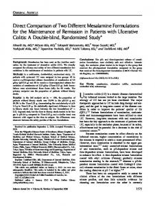
Fig. 1. Block diagram of the automated comparison between the two PJVS systems measured with an analog nanovoltmeter (NVM).
Fig. 2. Schematic of the waveform used to perform the synchronous switching between voltages (A: start 0 V to 10 V, B: from 10 V to 10 V, and C: from 10 V to 10 V). The four clock pulses are shown in red. The data acquisition occurs once both PJVS output voltages are fully settled (gray areas).
Page 20 of 25
Fig. 3. Voltage differences measured at 10 V alternately for the two input polarities of the NVM (N=normal and R=reverse). The dither current (di=0.2 mA) does not affect the measurement, confirming proper quantization of the voltages provided by both systems over the 28 hours of the measurement sequence.
QUANTUM LOCKING RANGE
Fig. 4. Results for the automated comparison measurement at 10 V vs. the dither current applied to both PJVS arrays (N polarity only, NVM polarity reversal switch removed). The step width (0.9 mA) is comparable to the smallest quantum locking range measured independently for the two PJVS systems.
Page 21 of 25
Fig. 5. Allan deviation extracted from 8192 readings with a short on the NVM input (NVM on the 10 µV range DVM 1V range with 10 PLC). The 1/f noise floor of 0.1 nV is reached after one minute.
Fig. 6. Gain calibration and non-linearity (INL) of the NVM. (A) Deviation of the measured difference PJVS(1)PJVS(2) from the calculated voltage difference . The output voltage of PJVS(1) is adjusted to 10 V by slightly detuning the microwave frequency, while PJVS(2) is kept at 10 V. Measurement for each was repeated 6 times. The gain error of the NVM (slope) is 3·103 V/V. (B) Deviation from the fit (INL) of Fig. (A): The value and error reported for the INL are, respectively, the mean value and standard Page 22 of 25
deviation of the 6 readings displayed in plot (A). The two horizontal lines (±0.12 nV) show the k=1 interval of confidence (standard deviation) calculated from all the INL data measured.
Fig. 7. Measured voltage difference between PJVS(1) and PJVS(2) for different grounding locations. The error bars represent the standard deviation (k=1) obtained with a minimum of 30 individual readings for each voltage and grounding configuration.
Page 23 of 25
Fig. 8. Schematic of the leakage current path I1 and I2, through the equivalent leakage resistances to ground RL1 and RL2, associated respectively with PJVS(1) and PJVS(2). The leakage paths to Earth ground of each system are much more complex than the simplified RL1 and RL2 representations (see text). In this model, the current distribution is shown for four different Earth ground positions; (A) the ground is connected to the low side of the PJVS(1) array, (B) the ground is connected to the low input terminal of the NVM, (C) the ground is connected to the high input terminal of the NVM, (D) the ground is connected to the low side of the PJVS(2) array.
Page 24 of 25
Fig. 9. Measurement of the voltage difference (N polarity of the detector) with and without a 10 resistance inserted between the two high sides of the PJVS systems.
Fig 10. Measurement of the voltage differences for both polarities of the detector as a function of the PJVS voltage. The measurement circuit is floating from Earth ground potential.
Page 25 of 25