Automatic Defect Inspection of Patterned TFT-LCD Panels Using 1-D Fourier Reconstruction and Wavelet Decomposition
DU-MING TSAI*, CHUNG-YU HUNG Department of Industrial Engineering and Management, Yuan-Ze University 135 Yuan-Tung Road, Chung-Li, Taiwan, ROC
*Corresponding author. Email:
[email protected] Tel: +886-3-4638800 Ext. 2507 Fax: +886-3-4638907
Abstract Large-sized flat-panel displays have become increasingly important for use in PC monitors and TVs.
In this paper we have considered the problem of automatic visual
inspection of micro-defects including pinholes, scratches and particles in patterned Thin Film Transistor-Liquid Crystal Display (TFT-LCD) panel surfaces.
For large-sized
TFT-LCD panel inspection, high resolution line scan is demanded.
We propose a
global 1-D Fourier-based image reconstruction scheme that directly works on the 1-D line images, instead of the traditional 2-D area images.
The proposed method fully
utilizes the inherent geometric structure of a TFT-LCD panel.
It first eliminates the
frequency components that represent the periodic pattern of a TFT-LCD line image in the 1-D Fourier spectrum, and then back-transforms the 1-D Fourier-domain image to the 1-D spatial domain image using the inverse Fourier transform.
The Fourier
reconstruction process can effectively remove the patterned background and distinctly preserve local anomalies in the resulting 1-D image.
Wavelet decomposition is
further applied to remove uneven illumination in the filtered image so that defects can be easily segmented with simple statistical control limits. Experimental results on a number of micro-defects embedded in TFT-LCD panels show that the proposed method can reliably detect various ill-defined defects without designing and measuring the quantitative features of individual defect types.
Keywords: Defect detection; TFT-LCD; Line scan; 1-D Fourier transforms; Machine vision
1. Introduction Flat-panel displays have become increasingly important in recent years. They can be used as small viewfinders for handheld devices such as cellular phones and PDAs, and as larger monitors for notebook and personal computers.
Thin Film
Transistor-Liquid Crystal Displays (TFT-LCDs) are particularly attractive due to their full-color display capabilities, low power consumption and light weight. To ensure the display quality and improve the yield of LCD flat panels, the inspection of defects in TFT-LCD panels becomes a critical task in LCD manufacturing.
Surface defects of a TFT-LCD panel not only cause visual failure but also cause electrical failure to operate the panel. Appearance defects in TFT-LCD panels can be roughly classified into two categories: macro and micro defects (Nakashima 1994). Macro defects include unevenness of color on a TFT-LCD panel, stains on a panel, and misalignment of a panel.
Micro defects include pinholes, scratches and particles in a
TFT-LCD panel.
The macro defects appear as high contrast regions with irregular
sizes and shapes.
They are generally large in size and, therefore, can be detected by
human inspectors.
However, micro defects are generally very small in size, and cannot
be easily found by human personnel or detected with electrical methods.
There are currently several electrical and optical based inspection techniques available for TFT-LCD defect inspection (Kido 1992, Chen et al. 2000, Hawthorne 2000, Lin et al. 2001).
Kido (1993) and Kido et al. (1995) presented an optical charge
sensing technique for the inspection of active-matrix LCD panels.
Charge sensing
writes a charge to the storage capacitor at the individual TFT array pixel.
1
The charge
is read back and compared with the write charge to determine if the pixel is defective (Hawthorne 2000).
Henly and Addiego (1991) used an electro-optic modulator to
generate voltage images.
The voltage-imaging technique measures the characteristics
of a TFT-LCD array by directly measuring the actual voltage distribution on the TFT pixel and not at the storage capacitor. The advantage of the optical charge and voltage imaging approaches is that each pixel on the TFT panel can be individually tested. The main disadvantage of such approaches is that the probes used for voltage measurement must be separately designed for each panel configuration. With the fast development of LCD technologies, the new-generation polysilicon TFT-LCD displays with integrated drivers (Nakamura et al. 2002, Nishibe 2002) do not need storage capacitors.
The charge-sensing and voltage-imaging methods will become useless
since they cannot test arrays without storage capacitors.
A few vision-based techniques were developed for LCD defect inspection.
The
processing algorithm is typically either a computationally intensive pattern matching, or a more straightforward differencing method (Hawthorne 2000).
Nakashima (1994)
presented an inspection system based on image subtraction and optical Fourier filtering for detecting defects in an LCD color filter panel. The image subtraction method was utilized to detect white and black defects such as black matrix holes and particles, and the optical Fourier filtering was applied for grain defects.
Sokolov and Treskunov
(1992) developed an automated visual system for final inspection of LCDs.
They
compared brightness distributions between a reference LCD image and a test image to detect anomalies in the surface.
The existing vision-based techniques generally need a
pre-stored reference image for comparison. This requires large data storage for the
2
reference image and precise environmental controls such as alignment and lighting for the TFT-LCD panel under inspection. line-type defects in TFT-LCD panels.
Oh et al. (2004) studied the detection of In a low-resolution image, a directional filter
bank (DFB) that finds directional information is used to identify horizontal or vertical line-shaped defects.
In a high resolution image, a multi-level thresholding technique
based on a statistical approach is employed to detect abnormal line defects that are brighter or darker than the surrounding pixels. Their approach is only applicable to line-shaped defects.
Most of the vision-based techniques mentioned previously are based on the analysis of grey levels in two-dimensional area images.
Since there is an ongoing
strong demand for the TFT-LCDs used in large-screen PC monitors and TVs, large-sized TFT-LCD panel manufacturing is getting important.
For automatic visual
inspection of TFT-LCD panels, very high-resolution image acquisition will be mandatory.
High resolution line scan, therefore, will be demanded for the inspection
of large-sized TFT-LCD panels.
In this study, we propose an automatic visual
inspection scheme that identifies defects directly from one-dimensional (1-D) line images of TFT-LCD panels.
The proposed algorithms especially focus on the
detection of micro-defects including pinholes, scratches and particles in TFT-LCD panel surfaces.
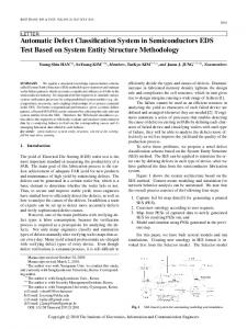
In the LCD manufacturing process, perpendicular data and gate conductive lines are patterned onto the glass substrate. A TFT-LCD panel comprises horizontal gate lines on one plane, and vertical data lines on the other plane. A thin film transistor is
3
located at each intersection of the data and gate lines (Pratt and Hawthorne 1998). Figure 1(a) shows the schema of a single pixel of a TFT-LCD panel (Kido 1993), and Figure 1(b) demonstrates the magnified two-dimensional (2-D) image of a TFT-LCD panel at the resolution of 60 pixels/mm. The geometric structure of a TFT-LCD panel surface involves repetitive, equally-spaced horizontal and vertical lines. Under a given resolution, the horizontal line patterns are repeated for every fixed number of the scan lines.
The repeated cycle corresponds to the vertical spacing between two adjacent
gate lines in a TFT-LCD panel surface. For each horizontal scan line, the distance between two adjacent peaks in the grey-level line image corresponds to the spacing between two neighbouring vertical data lines.
Each scanned line profile exhibits
periodicity and regularity properties. The problem of defect detection in TFT-LCD panel surfaces can now be considered as the identification of anomalies in a periodic 1-D grey-level signal. Note that the periodic pattern for each input line image is different to some extent, as seen in Figure 2.
The proposed method does not rely on the design of quantitative features to describe local anomalies, nor does it require a reference template for comparison. It alleviates all limitations of the feature extraction and template matching approaches.
It
is based on an image reconstruction scheme that directly works on the 1-D input images using the 1-D Fourier transforms.
The Fourier spectrum is ideally suited for
describing the periodicity of the TFT-LCD image signal in question. The proposed 1-D Fourier-based image reconstruction scheme fully utilizes the inherent geometric structure of TFT-LCD panels.
It first eliminates the frequency components that
represent the periodic peak pattern of the 1-D grey level profile of a TFT-LCD line
4
image in the 1-D Fourier spectrum, and then back-transforms the 1-D Fourier-domain image using the 1-D inverse Fourier transform. The Fourier reconstruction process can effectively remove the background of periodic peaks and distinctly preserve local anomalies in the resulting 1-D image.
For a faultless TFT-LCD line image, the
reconstruction process will result in a flat horizontal line. Conversely, high fluctuation of a line will be generated in the reconstruction for a defective TFT-LCD line image. The simple statistical process control limits can then be used to set up the thresholds for distinguishing between defective segments and uniform background in each reconstructed 1-D line image.
This paper is organized as follows. Section 2 first discusses the 1-D Fourier transform and the properties of one-dimensional TFT-LCD line images in the Fourier spectra.
The removal of repetitive background patterns in any scan lines of a
TFT-LCD panel is then analyzed. Section 3 presents the experimental results from a variety of TFT-LCD micro-defects including pinholes, scratches and particles.
Section
4 has conclusions of the paper.
2. The Fourier Reconstruction in 1-D Line Images 2.1. The 1-D Fourier transform The present study uses machine vision to tackle the problem of detecting microdefects embedded in TFT-LCD panel surfaces. The line images, instead of the area images, of a TFT-LCD panel obtained from a line scan system is directly used as the input for inspection in the manufacture of LCDs.
Each scanned line image shows a
periodic grey-level profile corresponding to the uniformly-spaced conductive data lines.
5
Figures 2(a-f) show a cycle of six line images for a faultless TFT-LCD panel at the resolution of 60 pixels/mm. The line images in Figures 2(a) and (b) are the grey-level profiles associated with horizontal gate lines in the TFT-LCD panel.
No significant
periodic peaks are observed in these two line images since they do not cross over conductive data lines.
Figures 2(c-f) are the scanned lines that cross over
equally-spaced data lines.
Visible periodic peaks are observed in the profiles, in which
each peak represents a data line.
For the sake of comparison, Figures 3(a1-f1), 3(a2-f2)
and 3(a3-f3) illustrate, respectively, six consecutive line images that cross over a pinhole, a scratch and a particle in TFT-LCD panels.
The corresponding 2-D
grey-level images of the three defect samples can be found in the experimental section of this paper.
Defects of pinhole, scratch and particle obviously break the regularity of
periodic structures and appear as local anomalies in the 1-D grey-level profiles.
In this study, the 1-D Fourier-based image reconstruction technique is directly applied to the 1-D grey-level line image to remove periodic peaks that represent data-line and gate-line patterns in TFT-LCD panel surfaces. The Fourier transform can characterize the line image of a periodic pattern in terms of frequency components. The periodically occurring features of data lines, gate lines, and TFTs of a TFT-LCD panel can be observed from the magnitude of frequency components. The global periodic pattern of a scan line is easily distinguishable as concentration of high-energy bursts in the Fourier spectrum.
Let f y (x ) be the grey level at pixel location x of a line image y , and N the length of a scan line. The one-dimensional discrete Fourier transform of f y (x ) is
6
given by
Fy (u ) =
1 N
N −1
∑ f (x ) ⋅ exp[− j 2πux / N ] y
x =0
(1)
for frequency variable u = 0, 1, 2,..., N − 1 . The Fourier transform is generally complex; that is
Fy (u ) = R y (u ) + jI y (u )
(2)
where R y (u ) and I y (u ) are the real and imaginary parts of F y (u ) , i.e.,
R y (u ) =
1 N
I y (u ) =
1 N
N −1
∑ f (x ) ⋅ cos(2πux / N ) x =0
y
(3)
N −1
∑ f (x ) ⋅ sin (2πux / N ) x =0
y
(4)
The power spectrum Py (u ) of Fy (u ) is defined by
Py (u ) = Fy (u )
2
= R y2 (u ) + I y2 (u )
(5)
2.2 Removal of periodic patterns
An arbitrary line image scanned from a faultless TFT-LCD panel surface consists
7
of periodic peaks in the grey-level profile. Each peak represents the location of an equally-spaced conductive data line on the plane. Let ∆x be the known spacing in pixel between two adjacent data lines (i.e., the distance between two neighbouring ∆x is the period of a 1-D spatial domain image.
peaks) in the line image.
The
relationship between the frequency components in the Fourier domain image and spatial characteristics of the 1-D grey-level profile in the spatial domain image is given by
∆u =
N ∆x
(6)
where N is the length of a scanned line image, and ∆u is the spacing between two adjacent peaks in the power spectrum.
For illustration, Figures 4(a) and (b) depict ∆x
and ∆u in a faultless line image of the TFT-LCD panel and the corresponding power spectrum, respectively.
In order to eliminate the periodic peaks that represent the data lines in the 1-D spatial domain image, the corresponding frequency components in the Fourier domain image are set to zero, and back-transformed to the spatial domain image using the 1-D inverse Fourier transform. Let U be a set of frequency peaks in the Fourier power spectrum, and
{
U = u1* , u 2* , ..., u n*
where u i* =
}
N ⎡ N ⎤ ± (i ⋅ ∆u ) , for i = 1, 2, ..., n and n = INT ⎢ . 2 ⎣ 2 ⋅ ∆u ⎥⎦ 8
The frequency
components u i* ' s and their neighbours defined by r are set to zero, i.e.,
Fy (u ) = 0 , for u i* − r ≤ u ≤ u i* + r ; i = 1, 2, ..., n
(7)
In this study, the r -distant neighbours are given by 3 at the image resolution of 60 pixels/mm.
With the newly assigned values of Fy (u ) , the 1-D spatial domain image
can be reconstructed using the 1-D inverse Fourier transform:
N −1
fˆy (x ) = ∑ Fy (u ) ⋅ exp[ j 2πux / N ]
(8)
u =0
Figures 5(e) and (f) present, respectively, the reconstructed results of the faultless line image in Figure 5(a), and the defective line image of a pinhole in Figure 5(b). These results exhibit that the periodic peaks representing the data lines in the TFT-LCD panel are well eliminated, while the anomaly associated with the pinhole defect is distinctly preserved.
Both reconstructed line images in Figures 5(e) and (f) present minor variations in the grey-level profiles. Given the Fourier spectrum of a 1-D grey-level image, the frequency components in the neighbourhood of the center of the Fourier spectrum are low frequency bands that represent the coarse approximation of the original signal, and those apart from the center are high frequency bands that represent the details. Figure 5(d) indicates that the frequency components corresponding to a local anomaly in the spatial domain are around the center of the Fourier spectrum. Since a defect results
9
from the local anomaly and the background contains a global repetitive pattern, the Fourier transform will inherently present the details of the global background pattern in high frequency bands and the unique local anomaly in low frequency bands in the Fourier spectrum. To smooth further the resulting 1-D grey-level profile from eqs. (7) and (8), the high frequency components outside the region defined by the parameter w (see Figure 4(b) for the notation) are also set to zero, i.e.,
Fy (u ) = 0 , for 0 ≤ u ≤ w and N − w ≤ u ≤ N − 1
(9)
Eqs. (7) and (9) are simultaneously applied for back-transforming the Fourier domain image to the spatial domain image using eq. (8). Figures 5(g) and (h) illustrate the final reconstruction results of Figures 5(a) and (b) by implementing both eqs. (7) and (9), where r = 3 is applied in eq. (7), and w is
3 N in eq. (9). The results 8
visibly reveal that all periodic peaks are effectively removed in both faultless and defective line images, while high fluctuation of grey levels associated with the defect is very well preserved.
Observing closely the resulting grey-level profiles in Figures 5(g) and (h), we find that the reconstructed line image yields significant grey-level variations in both ends of the profile, which may cause false alarms in defect detection of TFT-LCD panels. This is because that the implicit N -point periodicity of the DFT gives rise to boundary discontinuities that result in substantial high-frequency transform content (Gonzalez and Woods 2002). It causes the end points to take on erroneous values. In order to tackle
10
the problem of boundary discontinuities, each original line image is extended in both ends by duplicating their neighbouring grey-level segments of length ∆x (i.e., the spacing between two conductive data lines). That is,
f y (i − ∆x ) = f y (i ) , i = 0, 1, 2, ..., ∆x − 1 and
f y ( j + ∆x ) = f y ( j ) , j = N − ∆x, N − ∆x + 1, ..., N − 1
The newly extended grey-level line image is applied to the Fourier reconstruction, and only the resulting image in the range [0, N-1] is used as the effective profile for inspection. Figures 5(i) and (j) demonstrate that the extension procedure above can significantly improve the effect of boundary discontinuities.
2.3. Removal of uneven illumination
The proposed Fourier reconstruction procedure has shown its effectiveness on the removal of regularly-patterned background and the preservation of local anomalies in TFT-LCD panel images. However, as observed in Figure 5(i), the reconstructed line image is not a horizontal flat profile due to the unevenness of illumination on the TFT-LCD panel surfaces. This may cause the difficulty in the discrimination between uneven lighting and anomalies using simple statistical process control limits as the segmentation thresholds.
In this study, the unevenness of illumination is removed using the wavelet
11
transform.
The reconstructed 1-D grey-level profile fˆy (x ) is decomposed into
smooth and detailed parts using the Haar wavelet frame.
The discrete wavelet frame
decomposition with a Haar basis proceeds as follows.
sˆ y (x ) =
1 ∑ L( i ) ⋅ fˆy (x + i ) 2 i
1 dˆ y ( x ) = ∑ H ( i ) ⋅ fˆy ( x + i ) 2 i
(10)
(11)
where L( i ) and H ( i ) are the lowpass and highpass coefficients, respectively, of the Haar basis (Burrus et al. 1998).
sˆ y ( x ) is the decomposed smooth version of fˆy (x ) ,
which is an approximation of the original grey-level profile.
dˆ y ( x ) is the decomposed
detail version of fˆy (x ) , which entails only the fine detail of the original grey-level profile.
Note that both sˆ y ( x ) and dˆ y ( x ) have the same length of the original
grey-level profile fˆy (x ) because the filtered 1-D images are not subsampled. Figures 6 and 7 demonstrate the results of the wavelet frame decomposition from faultless and defective line images, respectively. It is apparent from Figures 6(c) and 7(c) that the smooth line image sˆ y ( x ) cannot remove the unevenness of illumination, and the detailed line image dˆ y ( x ) becomes flat for a faultless segment of a TFT-LCD line image, while the higher frequency oscillations corresponding to the defect segment is well signified in dˆ y ( x ) .
12
A simple dual thresholding based on the statistical process control limits can be therefore used to separate the defective segments from the uniform background in the decomposed detail dˆ y ( x ) . The upper and lower control limits for intensity variation in the decomposed detail image dˆ y ( x ) of a filtered line image fˆy (x ) are given by
µ dˆ ± K ⋅ σ dˆ y
where µ dˆ = y
1 N
σ dˆ = { y
(12) y
N −1
∑ dˆ x =0
y
( x) ;
1 1 N −1 ˆ [d y ( x) − µ dˆ ] 2 } 2 ; ∑ y N − 1 x =0
K = a control constant.
Note that the mean µ dˆ and the standard deviation σ dˆ of the decomposed detail y
y
dˆ y ( x ) are calculated for each individual scan line y , i.e., each input line image has its own control limits. In this study, we have used K = 3 for all scan lines to follow the typical 3-sigma standard in the statistical process control. Points in a uniform segment will lie within the control limits, and points in a defective segment will fall outside the control limits.
3. Experimental Results
In this section, we present experimental results from a variety of micro-defects including pinholes, scratches and particles in TFT-LCD panel surfaces to evaluate the
13
efficacy of the proposed 1-D Fourier reconstruction scheme.
To visualize the detection
results, the test images are displayed in two dimensions of size 256 × 256 pixels. That is, a 2-D test image comprises 256 scan lines, each of the length 256 pixels. The 3-sigma control limits were applied to all test images.
Points falling within and
outside the control limits are respectively represented by white and black intensities so that the detected defects can be easily observed and verified in the binarized image.
In
order to remove noise in the resulting binary image, a defect is assumed at least of the size 2 × 2 pixels. Therefore, a true defect must cross two consecutive scan lines at the same location in each of the two scan lines, i.e., a point at location x of a scan line
y is classified as a part of the defect only if both dˆ y ( x ) and dˆ y −1 ( x ) fall outside the control limits. This restriction can effectively remove isolated noisy points in the filtered image.
Figures 8(a-c) show, respectively, three defective 2-D images containing pinhole, scratch and particle blemishes in TFT-LCD panel surfaces at a fine resolution of 60 pixels/mm.
Figure 8(d) illustrates a faultless 2-D image at the same resolution. The
micro-defects of pinholes, scratches and particles can only be detected in images of fine resolution. They become blurred or invisible at resolutions under 50 pixels/mm.
Figures 9(a-d) present the detection results of the four test images in Figures 8(a-d), respectively. The 3-sigma standard is used for every scan line in Figures 8(a-d) to set up the control limits. Each one of the 2-D binary images in Figures 9(a-d) is the result of merging all the 256 filtered line images in their scanning sequence. In the defective images of Figures 8(a-c), pinhole, scratch and particles are well segmented. For the
14
faultless TFT-LCD surface image of Figure 8(d), the resulting binary image is uniformly white and no defect is claimed.
In order to demonstrate further the robustness of the proposed method under varying illumination, Figures 10(a1-e1) show five versions of a pinhole image (with some particles) under illuminations of 500, 1000, 1500, 2000 and 3000 Lux, respectively.
Note that Figures 10(a1) and (e1) are two highly underexposed and
overexposed images for inspection. Figures 10(a2-e2) depict the grey-level profiles of a scan line that crosses over the same region of the pinhole in Figures 10(a1-e1). The detection results as binary images are presented in Figures 10(a3-e3). They show that the defects of a pinhole and small particles are reliably detected for the test images under the illumination in the range 1000-2000 Lux. The pinhole and some particles can also be detected in the overly dark and bright images of Figures 10(a1) and (e1), except that their detected sizes are smaller and scattered.
In the proposed 1-D Fourier reconstruction scheme for TFT-LCD panel inspection, there are two parameters that affect the reconstruction results: the number of neighbouring points r of each peak u i* (see eq. (7)), and the high frequency region w (see eq. (9)) in the Fourier spectrum. w =
Empirical study has shown that r = 3 and
3 N give the best reconstruction results for the inspection images at the 8
resolution of 60 pixels/mm. In order to show that the proposed parameter values for r and w are not sensitive to varying line image length N , Figures 11-13 show additional test images of pinhole, particles, scratch, and a faultless surface in the lengths
15
of N = 256, 320 and 400 pixels.
It is apparent from the experiments that the
resulting binary images are uniform white for a faultless TFT-LCD panel image, and all defects are consistently detected with the same parameter setup, regardless of changes in the length N .
The parameters r and w used for the removal of periodic
patterns in line images of TFT-LCD panel surfaces, however, may have to readjust for TFT-LCD panels at different image resolutions. This is because the structural pattern of a TFT-LCD panel at different resolutions, both coarser and finer, may yield distinct periodic grey-level profiles.
4. Conclusions
The present paper has presented a 1-D Fourier image reconstruction scheme for automatic visual inspection of micro-defects in patterned TFT-LCD panel surfaces. The sensed image for inspection is assumed to be obtained from a line scan system. The proposed method can directly work on line images and, therefore, has the merit in inspecting large-sized TFT-LCD panels.
The proposed method neither requires the design of quantitative features for various defects, nor needs a prestored template image for comparison. It is based on a global approach using 1-D Fourier reconstruction.
By eliminating the frequency
components that correspond to the periodically structural patterns of a TFT-LCD panel, and then back-transforming the remaining frequency components to the spatial domain image, the regularly-patterned background in 1-D grey level profiles can be effectively removed.
A line image of a faultless region in the TFT-LCD panel surface will
become an approximately uniform grey-level profile, while the line image of a defective
16
region will be distinctly preserved in the reconstruction. The Haar wavelet frame decomposition is further applied to remove the effect of uneven illumination. Finally, simple 3-sigma control limits are employed to segment the highly deviated elements (i.e. defects) from the uniform background in the decomposed detail part of the Harr wavelet frame.
At the resolution of 60 pixels/mm, the appearances of pinholes, scratches and particles can be visibly observed in the images.
With the parameter values r =3
(number of neighbouring points of each peak in the Fourier spectrum) and w =
3 N 8
(the region of high frequency components) at the given resolution of 60 pixels/mm, the proposed method has reliably detected pinholes, scratches and particles. Experimental results also demonstrate that the proposed method is robust to detect the micro-defects under varying illumination conditions. The proposed method in this paper mainly aims at the detection of various micro-defects in TFT-LCD panel surfaces. It will be investigated in further research to classify the types of detected defects for in-process quality control.
17
References
Burrus, C.S., Gopinath, R.A., and Guo, H., Introduction to Wavelets and Wavelet Transforms: A Primer, 1998 (Prentice-Hall: New Jersey). Chen, P.O., Chen, S.H., and Su, F.C., An effective method for evaluating the image-sticking effect of TFT-LCDs by interpretative modeling of optical measurement, Liquid Crystals, 2000, 27, 965-975. Gonzalez, R.C. and Woods, R.E., Digital Image Processing, 2002 (Prentice-Hall: New Jersey). Hawthorne, J., Electro-optics technology tests flat-panel displays, Laser Focus World, 2000, 36, 271-276. Henly, F.J., and Addiego, G.., In-line functional inspection and repair methodology during LCD panel fabrication, SID Symposium Digest Paper, 1991, pp. 686-688. Kido, T., In-processing inspection technique for active-matrix LCD panels, in Proceedings of IEEE International Test Conference, Baltimore, MD., 1992, pp. 795-799. Kido, T., In process functional inspection technique for TFT-LCD arrays, Journal of the SID, 1993, 1/4, 429-435. Kido, T., Kishi, N., and Takahashi, H., Optical charge-sensing method for testing and characterizing thin-film transistor arrays, IEEE Journal of Selected Topics in Quantum Electronics, 1995, 1, 993-1001. Lin, C.S., Wu, W.Z., Lay, T.L., and Chang, M.W., A digital image-based measurement system for an LCD backlight module, Optics and Laser Technology, 2001, 33, 499-505. Nakamura, T., Karube, M., Hayashi, H., Nakamura, K., Tada, N., Fujiwara, H.,
18
Tsutsumi, J., and Motai, T., Low temperature poly-Si TFT-LCD with an integrated analog circuit, Journal of the Society for Information Display, 2002, 10, 203-207. Nakashima, K., Hybrid inspection system for LCD color filter panels, in Proceedings of the 10th International Conference on Instrumentation and Measurement Technology, Hamamatsu, 1994, pp. 689-692. Nishibe, T., Future for low-temperature polycrystalline silicon, in SID Conference Record of the 22nd International Display Research Conference, Nice, France, 2002, pp. 269-272. Oh, J.H., Kwak, D.M., Lee, K.B., Song, Y.C., Choi, D.H. and Park, K.H., Line defect detection in TFT-LCD using directional filter bank and adaptive multilevel thresholding, Key Engineering Materials, 2004, 270-273, 233-238. Pratt, W.K., and Hawthorne, J.A., Machine vision methods for automatic defect detection in liquid crystal displays, Advanced Imaging, 1998, 13, 52-54. Sokolov, S.M., and Treskunov, A.S., Automatic vision system for final test of liquid crystal display, in Proceedings of the IEEE International Conference on Robotics and Automation, Nice, France, 1992, pp. 1578-1582.
19
(a) (b) Figure 1. (a) Schema of a single pixel of a TFT panel (see Kido 1993); (b) Surface image of a TFT-LCD panel at the resolution of 60 pixels/mm.
20
300 250 200 150 100 50 254
231
208
185
162
139
93
116
70
47
1
24
0
(a) 300 250 200 150 100 50 254
231
208
185
162
139
116
93
70
47
24
1
0
(b) 300 250 200 150 100 50 254
231
208
185
162
139
116
93
70
47
24
1
0
(c) 300 250 200 150 100 50 254
231
208
185
162
139
116
93
70
47
1
24
0
(d) 300 250 200 150 100 50 139
162
185
208
231
254
139
162
185
208
231
254
116
93
70
47
1
24
0
(e) 300 250 200 150 100 50 116
93
70
47
24
1
0
(f) Figure 2. A cycle of six horizontal grey-level profiles for the TFT-LCD panel image in Figure 1 (b).
21
1
22
300 300 300
250 250 250
200 200 200
150 150 150
100 100 100
50 50 50
0 0 0
(e2)
(e3)
300
300
300
250
250
250
200
200
200
150
150
150
100
100
100
50
50
50
0
0
0 254
(d2)
254
0
231
254
231
(c2)
231
254
231
0 208
0
208
50
0
208
50
208
100
50
185
100
185
150
100
185
150
185
200
150
162
200
139
250
200
162
300
250
139
300
250
162
300
139
(b2)
162
254
231
208
185
162
139
0
139
0 116
50
0
116
50
116
100
50
116
100
93
150
100
93
(a2)
93
150
70
200
150
47
200
70
250
200
47
300
250
70
300
250
47
300
24
1
254
231
208
185
162
139
116
93
70
47
0
24
1
254
231
208
185
162
139
116
93
70
47
1 24
0
24
1
254
231
208
185
162
139
116
93
70
47
1 24
254
50
0
116
1 24
254
231
50
93
50
0
254
231
208
100
50
93
50
231
208
185
100
70
100
50
208
185
162
139
150
100
47
100
185
162
139
93
150
254
231
208
185
162
139
116
93
70
47
24
1
254
231
208
185
162
139
116
93
70
47
24
1
254
231
208
185
162
139
116
200
150
70
150
100
162
116
70
200
47
1
150
139
116
93
47
250
200
24
200
150
116
93
70
47
1 24
300
250
24
254
231
208
185
162
139
200
93
70
47
1 24
300
250
1
254
231
208
185
162
(e1)
139
(d1)
116
250
200
70
(c1)
116
300
250
47
1 24
(b1)
93
70
47
300
24
(a1)
93
70
47
24
0
1
254
231
208
185
162
139
116
93
70
47
1
250
24
1 24
300
1
254
231
208
185
162
139
116
93
70
47
24
300
(a3)
(b3)
(c3)
(d3)
(f1) (f2) (f3) Figure 3. Six consecutive line images that cross over a defect in the TFT-LCD panel: (a1-f1) pinhole, (a2-f2) scratch and (a3-f3) particle.
Py (u )
f y ( x)
∆u
∆x
x
0
N −1
0
w
N −w
N −1
u
(a) (b) Figure 4. The relationship between (a) ∆x in the spatial domain and (b) ∆u in the Fourier spectrum domain.
23
185
208
231
208
231
254
162
185
139
93
162
139
254
254
231
208
185
162
139
254
185 185
231
162 162
208
139 139
254
231
208
116
93
70
1
254
231
208
185
162
0 139
50
0 116
100
50 93
150
100
70
200
150
47
250
200
1
300
250
24
300
47
(h)
24
(g)
116
93
70
1
254
231
208
185
162
0 139
50
0 116
100
50 93
150
100
70
200
150
47
250
200
1
300
250
24
300
47
(f)
24
(e)
116
93
70
1
254
231
208
185
162
0 139
50
0 116
100
50 93
150
100
70
200
150
47
250
200
1
300
250
24
300
47
(d)
24
(c)
116
93
70
1
254
231
208
185
162
0 139
50
0 116
100
50 93
150
100
70
200
150
47
250
200
1
300
250
24
300
47
(b)
24
(a)
116
70
47
1
24
254
231
208
185
162
0 139
50
0 93
100
50 116
150
100
70
200
150
47
250
200
1
300
250
24
300
(i) (j) Figure 5. (a) A faultless line image of the TFT-LCD panel; (b) a defective line image of the pinhole; (c), (d) the respective Fourier power spectra of (a) and (b); (e), (f) the Fourier reconstructed images of (a) and (b), respectively, by setting the frequency components around the peaks u * ' s to zero; (g), (h) the final reconstructed images of (a) and (b) by further setting high frequency components to zero; (i), (j) the reconstructed images from the extended lengths of (a) and (b), respectively.
24
300 250 200
300
150 100 50 0
150
250 200
100
50 254
231
208
185
162
139
116
93
70
47
1
24
0
254
231
185
208
162
185
139
93
162
254
231
208
139
100
116
150
93
200
70
10 8 6 4 2 0 -2 -4 -6 -8 -10
250
47
300
1
(b)
24
(a)
116
70
47
1
24
254
231
208
185
162
139
93
0
116
70
47
1
24
50
(c) (d) Figure 6. Wavelet frame decomposition for a faultless line image: (a) grey-level profile of a faultless line image f y ( x ) ; (b) reconstructed image fˆy ( x ) ; (c) decomposed smooth part sˆ ( x) ; (d) decomposed detail part dˆ ( x) . y
254
231
208
185
162
139
116
93
70
47
1
0 24
162
185
208
231
254
185
208
231
254
139
162
50
139
100
116
150
93
200
70
250
47
10 8 6 4 2 0 -2 -4 -6 -8 -10
300
1
(b)
24
(a)
116
93
70
47
1
254
231
208
185
162
0
139
50
0 116
100
50 93
150
100
70
200
150
47
250
200
1
300
250
24
300
24
y
(c) (d) Figure 7. Wavelet frame decomposition for a defective line image: (a) grey-level profile of a pinhole; (b) reconstructed image fˆy (x ) ; (c) decomposed smooth part sˆ ( x) ; (d) decomposed detail part dˆ ( x) . y
y
25
(a)
(b)
(c) (d) Figure 8. Three defective images and their faultless version at the resolution of 60 pixels/mm: (a) pinhole, (b) scratch, (c) particles and (d) clear surface.
(a)
(b)
(c) (d) Figure 9. (a-d) Detection results as merged binary images for Figures 8(a-d), respectively.
26
300 250 200 150 100 50 0 1
24
47
70
(a1)
93
116
139 162
185
208 231
254
(a2)
(a3)
300 250 200 150 100 50 0 1
24
47
70
(b1)
93
116
139 162
185
208 231
254
(b2)
(b3)
300 250 200 150 100 50 0 1
24
47
70
(c1)
93
116
139 162
185
208 231
254
(c2)
(c3)
300 250 200 150 100 50 0 1
24
47
70
(d1)
93
116
139 162
185
208 231
254
(d2)
(d3)
300 250 200 150 100 50 0 1
24
47
70
93
116
139 162
185
208 231
254
(e1) (e2) (e3) Figure 10. Effect of changes in illumination: (a1-e1) A pinhole image under illuminations of 500, 1000, 1500, 2000 and 3000 LUX; (a2-e2) respective grey-level profiles of a scan image in (a1-e1); (a3-e3) detection results as merged binary images for the test images in (a1-e1), respectively.
27
(a1)
(a2)
(b1)
(b2)
(c1)
(c2)
(d1) (d2) Figure 11. Detection results from line images of length 256 pixels: (a1-d1) clear, pinhole, particles and scratch images for inspection; (a2-d2) detection results as merged binary images for (a1-d1), respectively.
28
(a1)
(a2)
(b1)
(b2)
(c1)
(c2)
(d1) (d2) Figure 12. Detection results from line images of length 320 pixels: (a1-d1) clear, pinhole, particles and scratch images for inspection; (a2-d2) detection results as merged binary images for (a1-d1), respectively.
29
(a1)
(a2)
(b1)
(b2)
(c1)
(c2)
(d1) (d2) Figure 13. Detection results from line images of length 400 pixels: (a1-d1) clear, pinhole, particles and scratch images for inspection; (a2-d2) detection results as merged binary images for (a1-d1), respectively.
30