Michael J. Flynn. Computer Systems Laboratory, Stanford University. Abstract. The evolution of microprocessor architecture depends upon the changing aspects ...
Basic Issues in Microprocessor Architecture Michael J. Flynn Computer Systems Laboratory, Stanford University Abstract
The evolution of microprocessor architecture depends upon the changing aspects of technology. As die density and speed increase, memory and program behavior become increasingly important in de ning architecture tradeo�s. While technology enables increasingly complex processor implementations, there are physical and program behavior limits to the usefulness of this complexity. Physical limits include device limits as well as practical limits on power and cost. Program behavior limits result from unpredictable events occurring during execution. Architectures and implementations that span these limits are vital to the continued evolution of the microprocessor. Keywords: microprocessor architecture, scaling, memory wall, cache limits, program behavior limits.
Successful microprocessor implementations depend upon the processosr architect's ability to predict trends and advances in both technology and user behavior. Selecting an approach for a microprocessor implementation depends on the architect's ability to correctly model the e�ect of new technologies, new applications, and new software and CAD tools. The most successful microprocessor implementations depend not simply on the use of the current state of the art in hardware algorithms, but more importantly in bringing together the knowledge of these algorithms together with projected advances in the technology and user state of the art. This note reviews some of the changing technology tradeo�s, and considers them in light of developments in algorithms, user behavior, and systems cost.
1 The Role of Scaling in Microprocessor Architecture The implementation technology of choice for microprocessors is CMOS. Improvements have been and continue to be made in reducing feature size. The smallest feature size generally corresponds to a dimension of the primary feature of a transistor device as implemented. This is sometimes called the drawn feature size. This feature size, f, is limited by mask resolution and the wavelength of the (ultraviolet) light used in the lithographic process to generate the device de nition. The movement to ever smaller device dimensions implies that signi cantly more devices can be implemented on a given silicon area. While current implementations use feature sizes of about f = 0:25�, it is projected that devices with feature sizes smaller than 0:1� can be available in the next few years. See Table 1 [11] for the Semiconductor Industry Association (SIA) projections on device characterizations for the next few years. For an architect, there are important implications to scaling. As feature sizes shrink, the area a device occupies shrinks as the square of the scaling factor. If the feature size is reduced by a factor of 2, a device need only occupy one quarter the area using the reduced feature size. 1
Journal of Systems Architecture'99
2
Table 1: 1994 SIA roadmap summary. Year of 1st DRAM Ship 1992 1995 1998 2001 2004 2007 Feature Size (�) 0.50 0.35 0.25 0.18 0.13 0.10 VDD (V ) 5.0 3.3 2.5 1.8 1.5 1.2 Trans/Chip 5M 10M 20M 50M 110M 260M Die Size (mm2 ) 210 250 300 360 430 520 Freq (MHz) 225 300 450 600 800 1000 DRAM Bits/Chip 16M 64M 256M 1G 4G 16G SRAM Bits/Chip 4M 16M 64M 256M 1G 4G Maximum power/chip (watts) 60 80 100 120 140 160 On the other hand, device speed is improved linearly with feature size. Thus, a reduction in feature size of a factor of 2 may (under constant eld assumptions) also reduce the device delay by a factor of 2. Local interconnection delay, however, does not scale by the same factor. To interconnect two points in a xed design shrunk by a factor of S on a side, the interconnect lengths will also be reduced by a factor of S (i.e., will shrink linearly). The RC delay per unit length associated with that interconnection will actually increase because of the reduced dimensions associated with the interconnection line. In an e�ort to mitigate this somewhat, most modern designs change the aspect ratio of the interconnection, as the wire size itself is shrunken [7]. That means that instead of both the thickness and the width of the line shrinking by the scale factor S, the thickness of the line may actually increase while the width of the line is shrunk by S. This changing of aspect ratio partially mitigates the e�ect of increasing RC, but certainly not completely. Thus, as scale factors reduce device sizes by 1=S 2 and reduce device delays by 1=S, interconnection delay between two points within a design is reduced only slightly. All this leads to designs that are interconnection limited. For purposes of this discussion, we assume that global interconnections are used for interfunctional unit interconnections, and not used for interconnections within a functional unit. Since cycle time and other basic parameters are largely determined by transit times or delays within a functional unit, for this discussion we assume that global interconnections (which may indeed scale as 1=S) have little direct e�ect on cycle time considerations and delays within functional units.
2 Implications of Scaling Feature Size 2.1 Cycle time SIA projects (Table 1) that, as feature size decreases, clock rates increase at a somewhat slower rate than we have seen in the past. This is because of the lack of linear scaling of local interconnects. Increasingly, functional unit designs are dominated by line delays, and not circuit delays. This may cause designers to rethink their selection of algorithms to implement various functional units. Implementations that use larger numbers of devices or larger number of devices in critical paths, yet o�er more regular layouts, reducing local interconnection delays, may be preferable to older implementations that stressed reduction of the number of gate delays in critical paths.
Journal of Systems Architecture'99
3
Still, we are not limited in our ability to create fast cycle times. Indeed, it appears that some current processor implementations are producing more aggressive cycle times than what would be projected by the SIA roadmap. Indeed, logical techniques such as wave pipelining, which uses sophisticated CAD tools to ensure balanced path delays, can be used to improve cycle time. Wave pipelining is based on the use of delay inherent in combinatorial logic circuits. Suppose a given logic unit has a maximum interlatch (clocked latches) of Pmax and a corresponding minimum delay of Pmin with clock overhead (setup, hold, skew, etc.) of C. Then the maximum achievable cycle time, �t, is �t = Pmax ? Pmin + C: As with conventionally clocked systems, the system clock rate is the maximum �ti over i latched stages. In practice, using special CAD tools [13], it is possible to arrange Pmin to be within about .8 to .9 of (Pmax +C). While this would seem to imply clock speedup of more than 5x, environmental issues (process variation, temperature gradient across a die, etc.) limit realizable clock rate speedup to about 3x [8]. As we will see later, cycle time is probably less important in processor implementations in the future than it has been in the past.
2.2 Memory Access Time As feature sizes shrink, memory designers have aggressively improved device density on chip and memory capacity per chip. For a single memory array, as array size increases, the interconnect line must span a larger number of devices. Since not all interconnections can be global, the access delay tends to be limited by local interconnects. Typically, the average access time has remained relatively constant as memory chip capacities have increased due to scaling of interconnects. Since processor cycle times have generally scaled with shrinking feature size, and memory access time has remained relatively constant, there is increasing pressure on the memory hierarchy| the cache and bu�ering subsystem|to compensate for the increasing number of processor cycles required to access memory on a line miss. There are several responses to this problem on the part of the memory designer. The rst is to design the memory chip so that it consists of not one array, but perhaps four (or n) arrays. Within each array, then, it may be possible to achieve some scaling advantage for improving access time. These \by n" designs can also be coupled with a second improvement. Since memory is usually implementated as a square array of cells, when access is made to a row of cells, rather than simply accessing a simple column bit as an output, one can rapidly move a sequence of bits starting at the originally accessed bit by temporarily storing the accessed row and making it available for fast sequential access mode. Neither of these techniques signi cantly improve the memory access time. The rst technique may improve the relative access time (as measured in processor cycles) to a memory cell slightly. The second technique transfers cache lines more rapidly from memory to cache.
2.3 The Memory Wall As processor speeds increase, the ratio of memory access time to process cycle time increases. The problem is compounded by the execution of multiple instructions in a single cycle. Suppose
Journal of Systems Architecture'99
4
we de ne the logical memory latency as the maximumnumber of instructions that are executable in a memory access time. The logical memory latency has signi cantly increased as processor cycle time improves and processors use enhanced instruction level parallelism. There is a maximum logical memory latency beyond which an application sees no performance advantage. In one form or another, this notion of a memory bound to processor performance has been referred to as the memory wall [10, 14]. It has been described as a latency or a bandwidth limitation of memory. Using large cache sizes to avoid the memory wall is limited. For large caches at least, in order to reduce the hit rate, one is naturally inclined towards using large line sizes. Large line sizes increase the bandwidth required of memory. Burger [1] shows that there is a signi cant opportunity to increase e�ective pin (and memory) bandwidth between one and two orders of magnitude by making better use of on-chip memory. The basis for this improvement is adapting the cache organization (line size, associativity and write policy) to the application. The most important lesson is that large caches blindly implemented (without reference to the application) are not a solution to processor performance.
2.4 Cache Limits Small feature sizes coupled with rather larger die size enable large (> 1 MB) on-chip caches, but these caches are limited in two ways: 1. Large caches cannot be accessed at the fast processor cycle times (e.g., �t � 1 nsec). 2. Applications limit the e�ectiveness of large caches. McFarland [7] has proposed an access time model for caches with feature size f in microns, size C in Kbytes, and associativity A as (approximately): ? � Access time (ns) = (0:35 + 3:8f + (:006 + :025f)C) � 1 + :3(1 ? 1=A3) : At f = 0:1�, we expect cycle time (�t) to be 1 nsec (Table 1). The cache model [7] suggests that at f = 0:1�, we could have a maximum cache size of � 32KB , direct mapped, with access time 1 ns (one cycle). � 128KB , direct mapped, with access time 2 ns (two cycles). The cache access in a processor cycle time problem can be managed with multiple levels of on-chip cache. At f = 0:1�, one might argue for even three levels of on-chip cache. The designer can have the area (for large caches) or the access time (to match fast cycle times), but not both. Notice that when feature sizes were greater than 0:5�, cache sizes were generally limited by chip area. At f = 0:1�, chip sizes are limited by cycle time as interconnect delays dominate the cycle time. The obvious alternatives are multicycle cache access times and relatively larger cache sizes, or small cache sizes coupled with multilevel on-chip cache. While it is relatively easy to improve cycle time, the advantage of such improvements are limited. Since memory access time does not scale with processor cycle time, increasingly processors become memory limited. The technology to bridge this speed di�erence involves multiple levels of cache, but cache can be limited by exactly the same interconnection limitations that limit memory, forcing fast caches to be relatively small and forcing the architect to use multiple levels of on-chip cache to attempt to match the memory access time with the processor cycle time.
Journal of Systems Architecture'99
5
3 Power and Power Density in Microprocessor Architecture Chip power and systems power play important roles in determining both cost and performance of a microprocessor implementation. The SIA roadmap points to increasingly higher power for microprocessor chips. This implies a return to older mainframe and supercomputer type of cooling technology, with heat exchanges or liquid immersion. At a device level (or with scaling on a power-density basis), the power is 2 P = CV 2(freq) ; where C is the device capacitance, V is the voltage and (freq) is the frequency of operation of the device. If we lower the frequency of an existing design, we scale the power linearly with frequency. However, there is an important distinction for scaling power between the existing design and a new design|a power optimized design in which the frequency is reduced to optimize total power consumption. A simplistic way of understanding this di�erence is to imagine that we took an existing design that has been optimized for frequency and we modify that design simply by changing the circuits so that they could operate at half the voltage. This has the e�ect (to a rst order) of also having the frequency, but the resultant design would reduce the power by the cube root of the original power. While this analysis is simplistic, as reduced power implementations rarely just halve the voltage, empirically it seems that power optimized designs (operating with power P1 and frequency freq.1 ) in fact can be characterized by a cube root law: r
freq2 � 3 P2 : freq1 P1 For example, if we increase the power (Pr) by 8x (over P1), we expect to double the clock frequency. Power optimized implementations di�er from performance optimized (power P2 and frequency freq2) implementations in a number of ways: the implementations use less chip area not only because of less requirements for power supply distribution and clock distribution, but more importantly because of reduced performance targets. In performance oriented microprocessor designs, a great deal of area is consumed in achieving marginally improved performance|very large oating point units, or maximally sized caches.
Power optimized designs become increasingly important in any type of battery powered or portable implementations. As this is an important growth area for microprocessors, area optimization and power optimization are closely related. The understanding of this relationship and architectures which satisfy various optimization criteria are an important issue moving forward in microprocessor architecture.
4 Limits on Scaling Somewhere below f = :10�, probably at feature sizes greater than f = :05�, there are physical barriers to simply scaling CMOS circuits as we have done over the past decade.
Journal of Systems Architecture'99
6
There is an obvious concern with both the cost and di�culty in simply providing the lothography to realize devices below .10� in size. That structures can be produced with these sizes is not in question, but the cost of doing so has been raised as a limitation on the ultimate feasibility of doing so. Additionally, there are other problems which arise in this same region [7]. Very thin oxide layers (the oxide scales with the device size) and very small channel widths may compromise the long term stability of some of the dielectric materials and some of the device structures themselves. Additionally, very small structure sizes may result in unacceptable ratios of on{o� current values. Similarly, scaling voltages down to one volt or below may prove di�cult or impossible, since it requires that the switching threshhold voltage must also be scaled and this value also be maintained as a reasonable constant during the device performance. Over the years, device engineers have gotten around many problems, some as formidable as the above. The argument here is not that these limits will impose fundamental realization limits on devices, but rather that the scaling laws and the way architects have anticipated changes in technology may have to be completely reexamined based on the solutions that the device engineers come up with at this point. Some of their problems can be avoided, for example, by maintaining very low junction temperatures across the chip (cool CMOS). Devices chilled to liquid nitrogen temperatures are known to have signi cantly enhanced performance. Similarly, devices operating in the subthreshhold region (always cut o�) use extraordinarily low currents and have therefore low power operation. This is the same technology that is used in microprocessor-based watch implementation, where the total power consumed is on the order of microwatts. Of course, operating in the subthreshhold region usually involves what we now think of as extraordinarily slow cycle times|on the order of perhaps 10 Mhz. Over the years there have been a consistent number of predictions and projections that would point to fundamental limits beyond which our familiar silicon-based technology could not go. Each time, however, technologists have been able to engineer their way around these limitations, moving ahead to new limits. Physical limits again approach in the so-called deep sub-micron region (somewhere between .05� and 0.10�). The architect must realize that as these limits are approached, the technologist may make compromises or changes that are not a direct scaling of our current technology. Changes like this, if and when they occur, are important challenges to the processor architect to quickly understand the implications of the changes and then to use these changes to best advantage.
5 Program Behavior Limits It is generally, but not always, true that processors with faster cycle times provide better overall performance. Consider the case of a simple pipelined processor. For these simple pipelined processors, an estimate of the optimum number of stages in a pipeline has been determined [3] as Sopt : r
T.
(1) Sopt = (1 ?bCb)T : The b term represents the fraction of instructions that cause a pipeline \break" of duration
Journal of Systems Architecture'99
7
The ratio C=T is simply clocking overhead (C) per cycle as a fraction of total instruction execution latency (T). If we make the cycle time too large and have too few stages in the pipeline, we sacri ce overall performance. On the other hand, if we make the cycle time too small, we incur increasing amounts of clock overhead and we su�er from additional long pipeline breaks. One can imagine an analogous equation to describe the selection of a optimum level of ILP, ILPopt : r
(2) ILPopt � (1 ?d d) � O1 : This relationship is developed strictly as an analog to Sopt in equation 1 as the exact form of ILPopt depends on the underlying processor architecture assumptions. Here, O is the overhead of adding another instruction to an ILP machine as a fraction of the total instruction execution. It is assumed that O is constant for each additional instruction added. The parameter d is the fraction of occurrence of signi cantly disrupting events (akin to a misguessed branch) which causes the ILP machine to have to restart with a new instruction count. The tradeo� between VLIW and superscalar machines [2] is simply the tradeo� between reducing overhead with a VLIW machine and potentially nding potential parallelism and hence reducing the disruption with a superscalar machine. As before, latency tolerance reduces for all organizations d, the probability of a disruption, and hence improves the ILP available. For either processor approach (fast �t or increased ILP), the performance is bounded by implementation overhead and program behavior. We can use our understanding of algorithms to advance both of these limits. Non-predictable events, whether they be mispredicted branches, data dependencies, limited ILP, or resource contention, provide a strong limit to what the architect can do in designing a processor. Attempting to push these limits upward and improve performance is very di�cult. Improving the prediction rate for branches over a simple history bit based scheme is extremely di�cult and costly [15]. A great deal of addiitonal die complexity must be introduced to even marginally improve the prediction rate of branches or to accommodate dependencies across branches. There has been recent discussion of the possibilities of making the ILP more visible to the software for better management. This is historically a reasonable approach, especially when the architect is in danger of overwhelming the performance of the processor with complex and perhaps marginally valuable hardware. It is a slippery slope when one overreaches and segments the pipeline beyond Sopt or attempts to create an ILP greater than ILPopt . The designer can have the worst of all worlds: poor performance and very high cost. Simplifying the hardware and placing the responsibility of achieving high levels of concurrency on the software is a reasonable alternative. Several generations of very successful vector processors are based exactly on this principle. Indeed, it may well be that the vector architecture, long the backbone of mainframes and supercomputers, may have a role in microprocessor architectures. The emergence of \MMX" instructions with a type of subword parallelism is in fact a simple form of vector instructions oriented to a particular application. Of course, the limitations of vector processors are well known. The speedup is rather limited (perhaps to twice a pipeline processor), and the memory accessig problems can be formidable. But surely no worse than any other type of highly concurrent processor.
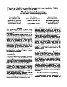
Journal of Systems Architecture'99 Multiprogramming level = 10 Line size = 16 bytes
1
Miss rate
8
Q 100 1K 10K 20K 100K
.1
Single user plus op.sys. effects Design target miss rate [14] .01 10
100
1K 10K Cache size
100K
1M
Figure 1: Miss rate for a warm cache with ten tasks (MP = 10). Ultimately, the e�ectiveness of cache is heavily dependent on the application. In an application consisting of a large number of small transactions, a system cannot e�ectively use a large cache, as before the cache lls, the transaction is complete and the application moves on to another process. The number of instructions between a task switch (Q) has been used as a measure of stability or latency tolerance of an application [12]. Figures 1 and 2 [4], show two multitasked environments, one where control is never returned to a task (a cold or transaction environment), and another where, in high degrees of multiprogramming applications, control does return to an application (this is called a warm cache environment). If applications are indeed latency tolerant, then high degrees of instruction issue and large caches make a great deal of sense. If applications are latency intolerant, such as a transaction or a highly multitasked environment, then the systems become completely memory limited, and the exact processor organizational details are not signi cant.
It is exactly in the server area where performance is at a premium that we frequently encounter a transaction type environment. If we are simply multiprogramming, there may be a solution in either multithreaded multiprocessors on chip, or simply multiple processors on chip where each processor assumes management of a small number of tasks or threads. On-chip multiprocessing [9] may o�er designers an interesting alternative to ILP in improvement in overall systems performance.
6 Cost The last basic tradeo� exists in determining an optimum die size [4]. A die yield is a function of both defect density (�D ) and the die area, A. In a simple Poisson model, the yield is Yield = e?�D A
Journal of Systems Architecture'99 10
9
16-byte line, 4-way associative
0
Q 100
Miss rate
1000 10000 10
20000
-1
100000
Single user plus op. sys. Design target miss rate 10
-2 10
1
10
2
3
4
10 10 Cache size (bytes)
10
5
10
6
Figure 2: Miss rate for a cold-start cache including system activities. and the number (N) of die per wafer (diameter d) is 2 N = �d 4A : If Ng is the number of good chips, then Yield = NNg : A typical defect density is about one defect per square centimeter. Die cost is determined by dividing the wafer cost by the number of good chips realized on the wafer. As die area increases, both the total number of chips on the wafer decrease, and the number of good chips decreases as the yield decreases. An increase in die area of 2 can easily lead to an increase in die cost of 10. Since there is a xed packaging testing cost associated with each die, making a die very small does not signi cantly decrease overall packaged die costs; indeed, having too little functionality on the packaged die decreases the attractiveness of the part to the buyer. This decreases the production run of the part and increases costs. Currently, most processor dies have area between 1.0 and 3.0 cm2. The element of cost creates a cleavage in processor designs. In what can be termed the server market, the processor may be a relatively small component in a much more costly system dominated by costs of memory and storage, etc. In this design area, an increase in processor cost of ten times (from, say, die cost of $10 to dies cost of $100) may be not very signi cant in the overall systems cost. Most processor implementations are more cost sensitive. These processors we could term client processors, and include processors devoted to end-user applications|embedded processors, personal computers and network computers. For these processors, the optimum use of area is
Journal of Systems Architecture'99
10
very important. As technology and costs allow, there will be an increasing need for increasing functionality within the processor so as to incorporate various signal processing (multimedia and graphics) and memory functions that now are assigned to separate chips. This notion of a systems chip is very important in future microprocessor architectures. Server processors will continue to be enhanced with signal processing capability (multimedia, etc.) but the server processor is never an ideal basis for the client processor, since it has not initially made the same cost tradeo�s that must be made for an optimum client implementation. This is especially true in the area of power and the inclusion of items of marginal performance enhancement. Ultimately, the client processor is the systems chip, however. The system or client chip is not simply a processor plus a variety of signal processors plus memory; it must be a carefully crafted processor with signal processing capabilities wherein those capabilities are carefully adapted and adaptable to various application requirements during the course of execution of a workload.
Conclusion As technology scales, there are important new opportunities for microprocessor architects. The simple traditional measures of processor performance|cycle time and cache size|are becoming increasingly meaningless in correctly evaluating application performance. Some of the most signi cant challenges facing the microprocessor architect now include: 1. Creating high performanc eprocessors jointly or cooperatively with enableing compiler software. Whether the resultant architectures are vector processors, VLIW, or other type, it is important that the processors really deliver the speci ed performance across a spectrum of applications. 2. Not explicitly discussed in this paper, but of great importance, is attention to features that preserve the integrity of computation, reliability, and diagnostic features. 3. The increasing use of adaptability in various processor structures such as cache and signal processors. For example, an adaptive cache would not just simply prefetch, but would prefetch according to a history of accessing behavior on the part of the particular program. Similarly, we could see adaptability in arithmetic, where arithmetic functional units can be rede ned, perhaps with the assistance of FPGA elements in function and performance to suit various applications. Microprocessor architecture promises to be as exciting in the future as it has been in the past.
Acknowledgements Some of the ideas expressed in this paper have been previously presented in conferences [5, 6]. This research was supported in part under NSF Grant MIP93-13701.
Journal of Systems Architecture'99
11
References [1] D. Burger, J. R. Goodman, and A. Kagi. Memory bandwidth limitations of future microprocessors. In Proceedings of ISCA'96, pages 78{89. [2] M. Butler and Y. Patt. An investigation of the performance of various dynamic scheduling techniques. In Proceedings of MICRO-25, December 1992. [3] P. K. Dubey and M. J. Flynn. Optimal pipelining. Journal of Parallel and Distributed Computing, 8:10{19, 1990. [4] M. J. Flynn. Computer architecture: Pipelined and parallel processor design. Jones and Bartlett, Boston, 1995. [5] M. J. Flynn. \What's Ahead in Computer Design?" Invited keynote. In Euromicro'97 Proceedings, pages 4{9, Budapest, September 1997. [6] M. J. Flynn. \Time and Area Optimization in Processor Architecture." Invited keynote. In Proceedings of ARCS'97, pages 1{9, Rostock, Germany, September 1997. [7] G. McFarland. CMOS technology scaling and its impact on cache delay. PhD thesis, Stanford University, 1997. [8] Kevin Nowka. High performance CMOS system design using wave pipelining. PhD thesis, Stanford University, August 1995. [9] K. Olukotun, B. Nayfeh, L. Hammond, K. Wilson, and K.-Y. Chang. The case for a single chip multiprocessor. In Proceedings of ASPLOS VII, pages 2{11, October 1996. [10] A. Saulsbury, F. Fong, A. Nowatzyk. Missing the memory wall: The case for processor/memory integration. In Proceedings of ISCA'96 pages 90{100. [11] Semiconductor Industry Association. The National Technology Roadmap for Semiconductors. San Jose, CA, 1994. [12] A. J. Smith. Cache memories. ACM Computing Surveys, 14(3):473{530, September 1982. [13] D. Wong, G. De Micheli and M. Flynn, \Algorithms for Designing High-Performance Digital Circuits Using Wave Pipelining," IEEE Transactions on CAD/ICAS, pages 25-46, January 1993. [14] W. Wulf and S. McKee. Hitting the memory wall: Implications and the obvious. ACM Computer Architecture News vol. 13 no. 1, March 1995. [15] T.-Y. Yeh and Y. N. Patt. Two-level adaptive training branch prediction. In Proceedings of the 24th Annual International Symposium on Microarchitecture, pages 51{61, November 1991.
Journal of Systems Architecture'99
12
is professor of electrical engineering at Stanford University, where he founded the Computer Emulation Laboratory, which has been a leading facility for the analysis of computer architecture. Current research projects include programs on ultra-high-speed arithmetic performance, rapid evaluation of computer architectures, and parallel machines. Dr. Flynn has served on the IEEE Computer Society Board of Governors and as Associate Editor of the Transactions on Computers. He was founding chairman of both the ACM Special Interest Group on Computer Architecture and the IEEE Computer Society's Technical Committee on Computer Architecture. He was the 1992 recipient of the ACM/IEEE Eckert{Mauchly Award and in 1995 received the IEEE{CS Harry Goode Memorial Award. Flynn worked at IBM for ten years in the areas of computer organization and design. He was design manager of prototype versions of the IBM 7090 and 7094/II, and later for the System 360 Model 91 CPU. He received his Ph.D. from Purdue University in 1961 and holds an honorary D.Sc. from Trinity College, Dublin. Michael J. Flynn


![[PDF] Download Microprocessor Architecture ... - Google Sites](https://m.moam.info/img/260x300/pdf-download-microprocessor-architecture-google-si_64771855097c4796708b529f.jpg)

![[PDF] Download Microprocessor Architecture ... - Google Sites](https://m.moam.info/img/260x300/pdf-download-microprocessor-architecture-google-si_6477a664097c4796708befb4.jpg)