CCD/CMOS Lock-In Pixel for Range Imaging: Challenges, Limitations and State-of-the-Art Bernhard Büttgen*, Thierry Oggier, Michael Lehmann, Rolf Kaufmann, Felix Lustenberger Swiss Center for Electronics and Microtechnology, Badenerstrasse 569, 8048 Zurich, SWITZERLAND Abstract Smart lock-in pixels for real-time range imaging have been developed at CSEM during the last few years. These pixels, based on a combined CCD/CMOS process, are capable of demodulating intensity-modulated optical signals in parallel. By integrating some hundreds or thousands of them on one single chip, real-time 3D-imaging becomes possible by indirectly measuring the time-of-flight. The basic challenges and requirements of the pixels, making them usable for a wide range of 3D-applications, are the handling of strong signal variations over the imaged scenery, background light suppression techniques and high distance accuracy. These challenges and according difficulties in real implementations are discussed. Limitations of the pixels, both physically as well technologically, are derived and the basic need for current and future research and development is shown. The state-of-the-art pixel, as implemented in the so-called SwissRanger camera, is used for demonstrating the nature of the before mentioned challenges and limitations. Keywords range image, time-of-flight, lock-in, CMOS/CCD, challenges, limitations, dynamic range, background light, charge transport
1. INTRODUCTION Many applications, such as robotics, biometrics, automobile security and navigation, medical imaging, surveillance and so on, require a three-dimensional representation of the environment to avoid the time-consuming processing steps required in order to ensure the high quality of the specific task. As a consequence, real-time 3D-imaging has become one of the most important challenges in the design of modern electronic image sensors. Thereby, the acquisition of 3D-data with optical systems is favoured over alternative methods based on ultra-sonic or radar for many applications. The reason is that optical systems allow for very fast 3D-data acquisition, an (eye)-safe system set-up and a high lateral resolution. Furthermore, the exploitation of the photo-effect in silicon material enables the realization of cost-efficient electronic 3D-sensors. Optical cost-efficient real-time 3D-cameras are hardly realizable with standard well-known acquisition techniques that are based on either scanning systems or stereo-systems with complex filtering and correlation processing units. Moreover, real-time 3D-imaging needs pixel-matrices composed of “smart” pixels where each pixel is simultaneously capable of delivering the distance information of one point in the scenery. Neither a scanning component nor a complex calculation unit for the distance map should complicate the set-up or lead to an additional processing time-delay, respectively. The need for such 3D-pixels has been investigated already in the early 90s and the investigations resulted in the so-called lock-in pixels, which are presented herein. The lock-in pixels are capable of demodulating an optical wave impinging on the sensor. Based on the time-of-flight principle, the demodulation parameters of the wave, in particular
the phase information are used for the extraction of the distance information to one point in the scenery. The underlying principle of time-of-flight distance measurement with a continuouslymodulated optical signal is briefly described in section 2. After that, section 3 introduces the specific architecture and functioning of the lock-in pixel used for the demodulation process. Section 4 points out the challenges in the design of the pixel when targeted for a highresolution pixel matrix sensor. Both physical as well as technological limitations are described as well. In order to overcome some of the challenges, enhanced lock-in pixel structures have been developed. They are briefly discussed in section 5. Finally, the main aspects of the present paper are summarized in section 6 and a conclusion is provided.
2. TIME-OF-FLIGHT DISTANCE MEASUREMENT The time-of-flight (TOF) technique is one possible method for the fast optical acquisition of distances. Its classification into the wide range of techniques for high-speed optical distance measurement is briefly treated in the first subsection. After that, the basic principle of time-offlight measurement is pointed out and the demodulation by natural sampling is reviewed.
2.1. Classification of TOF Figure 1 shows the raw classification of distance measurement methods. Three methods are distinguished: [1][2] 1. Triangulation: The geometrical relations between the object, the sensor and a known basis line are used for the calculation of the distance. The acquisition of 3D-images without scanning components is done by stereoscopy, meaning the clever combination of two 2Dimages from different points of view. The processing of the distance maps is based on correlation calculations that are strongly time-consuming. [1][2] 2. Interferometry: Constructive and destructive superpositions of at least two light beams are exploited for measuring very small differences of distances in the sub-micrometer range. Accordingly, the accuracies are very high and mainly depend on the coherence length of the light source. Real-time 3D-imaging is possible using modern CMOS photo-sensors [8]. Thereby, the imaging process is reduced from three scanning directions to just one scanning direction. However, interferometry is not suitable for ranges starting from some centimetres up to several meters as the method is based on the evaluation of the very short optical wavelength. 3. Time-of-flight: The time that the light needs to travel from the measurement system to the object and back again corresponds directly to the distance R, and is called time-of-flight (TOF): 2R TOF = , equation 2.1 c where c is the light velocity (c=3*108m/s). The method is very suitable for ranges starting from some centimetres to several hundreds of meters with relative accuracies of 0,1%. That means that standard deviations in the millimetre range are realistically achievable at absolute distances of some meters, corresponding to a time-resolution of 6.6 pico-seconds. Parallel measurement to some thousands of points in the three-dimensional scenery can be realized with image sensors based e.g. on “smart” demodulation lock-in pixels. [3]
contactless distance measurement
Triangulation
Interferometry
Time-of-Flight
Continuous wave modulation
Pulse
Figure 1: Overall classification of the time-of-flight principle within the techniques of three-dimensional imaging
The TOF can be measured either directly or indirectly. Consequently, it is distinguished between two different time-of-flight methods, as depicted in Figure 1: • A light pulse is sent out and its turn-around time is measured directly. • A continuously-modulated, e.g. sinusoidally modulated, light wave is emitted and the phase delay ϕ between the original and received light signal is exploited for the extraction of the time or distance information. The latter method of continuously-modulated (CW) time-of-flight measurement incorporates much lower requirements to the electronic components (e.g. frequency bandwidth, signal generation, etc.) as the operation point of the system is limited to just one frequency, namely the modulation frequency. The principle of CW-TOF is shown in Figure 2. The left figure depicts the whole system set-up, comprising a modulated light source, the scenery which reflects the light signal, the detector array of lock-in pixels and a control unit. Appropriate software tools are used for the data transfer to the PC, the filtering and the visualization. In Figure 2b, the relation between the emitted and received optical modulation signals Pe and Pr points out the fundamental signal behaviour of the overall measurement system: • The phase shift ϕ is the result of the signal round-trip from the measurement system to the scenery and back. It is exploited for the extraction of the distance information. • The received signal is offset-shifted by a mean optical power PB mainly due to additional background light and a non-perfect demodulation. The offset component describes the intensity information. • The amplitude of the detected optical signal component is reduced by a factor k, depending on all optical losses. Its height defines the signal-to-background ratio and hence the achievable accuracy is determined. The emitted mean power of the signal is expressed by PA, so that the amplitude of the received signal corresponds to k * PA.
Control unit
Popt R
In-pixel distance measurement
optical power Pe & Pr
scenery emitted signal received signal k ⋅ PA
ϕ
PA
PB
time
a) Time-of-flight measurement system b) emitted and received optical modulation signals Figure 2: Principle of the time-of-flight measurement based on continuously sinusoidally modulated signals
2.2. Demodulation by Sampling By sampling the incoming sinusoidally-modulated optical signal four times per modulation period with each sample shifted by 90 degrees, the modulation signal can be reconstructed unambiguously. Each sample corresponds to the integration of the photo-generated charge carriers over a fraction of the modulation period. This technique is called a natural sampling process. The summation of each sample over several modulation periods increases the signalto-noise ratio. E.g., using a modulation frequency of 20MHz and a summation over 10ms means that each sampling can be integrated over 200.000 modulation periods. Based on the four samples A0, A1, A2 and A3, the three decisive signal parameters offset B, amplitude A and phase ϕ can be extracted: A0 + A1 + A2 + A3 Offset B= equation 2.2 4
Amplitude Phase
A=
( A0 − A2)2 + ( A1 − A3)2
2 ⎛ A0 − A2 ⎞ ϕ = atan⎜ ⎟ ⎝ A1 − A3 ⎠
equation 2.3
equation 2.4
A and B are represented by numbers of electrons. Whereby the offset describes the total intensity of the detected signal, also including background light, and the amplitude is a measure of the signal itself, the distance R is derived from the phase information (s. equation 2.3.): c R= ⋅ ϕ. equation 2.5 4 π ⋅ f mod Thereby fmod describes the modulation frequency.
2.3. Demodulation Contrast The quality of the pixel-inherent demodulation efficiency is given by the ratio between the amplitude and offset values when no background light is present. In this case the offset B corresponds to the mean number of electrons Asig generated exclusively by the signal component. Equation 2.6 shows the mathematical definition of that parameter: A A cdemod = = equation 2.6 without back B ground Asig light The theoretical maximum depends on the specific nature of the sampling process. The shorter the integration period, the higher the demodulation contrast can be. Considering an integration period of half of the modulation period, as it is implemented in the SwissRanger camera [6], the demodulation contrast can not exceed 64% following the signal theory of natural sampling. [3] In practice, the demodulation contrast of current lock-in pixels is about 50%. The decrease of the contrast is due to additional parasitic effects.
3. LOCK-IN PIXEL FOR OPTICAL TOF DISTANCE MEASUREMENT The lock-in pixel accomplishes the demodulation of the impinging optical signal by sampling the signal at four discrete time steps resulting in four samples A0, A1, A2 and A3. The integration of the photo-generated charges is performed over half of the modulation period for each of the four samples, validating the equations of section 2.2. Both the detection and the complete demodulation are done in the charge-domain using charge-coupled devices. That ensures an almost noise-free demodulation of the light signal and over a wide range of
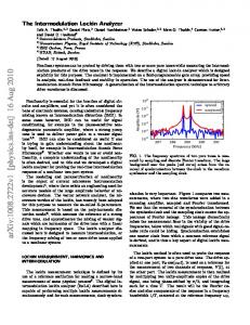
operation conditions results in distance accuracies close to the physical limitations. A closer look at the physical limitations is provided in the subsequent section. Figure 3a explains the pixel architecture and its sampling process. A symmetric subsequence of overlapping poly-silicon gates forms the demodulation pixel that delivers two samples of the impinging optical signal at the same time. The generation of the charges takes place below the left, right and middle photo-gates (PGL, PGR, PGM). Applying appropriate control voltages to the photo-gate, a characteristic potential distribution is built up in the buried channel forcing the charges to drift to the left or right side. On each side, the charges are stored below an integration gate (intg). The left and right photo-gates are toggled synchronously with the modulation frequency so that each charge packet below one integration gate corresponds to one sample of the light signal. In order to read out the charge packets, the voltage on the integration gates is decreased so that the accumulated charges will drop over the out gate (outg) into the sensing diffusion (diff). Standard source follower circuits in complementory-metal-oxide-semiconductor-(CMOS-) technology, implemented within the pixel but not shown in Figure 3, do the necessary amplification of the diffusion voltage for high speed read-out. Figure 3b shows the top view of the pixel. In order to demodulate at frequencies of some tens of Megahertz, the transport paths of the photo-generated charges have to be kept as short as possible. As a consequence, the sensitive area can only be increased by stretching the gates in just one direction, as can be seen in the top view of the pixel.
a) Simulated cross section and potential distribution
b) Top view
Figure 3: Architecture of the lock-in pixel; a) The cross section shows the symmetric CCD gate structure of the outgate, integration gate and photo-gate. On both sides, the diffusions are designed for reading out the accumulated charge packets. In the middle, a third transparent photo-gate is situated. Also given is the simulated potential distribution in the buried channel for two different voltage b) the top view illustrates the longitudinal stretched gate structures
4. TOF RANGE IMAGER - CHALLENGES AND LIMITATIONS Depending on the particular application or operational environment, a 3D-TOF range imager needs to fulfill different aspects at the same time. E.g. in the sector of gaming or virtual reality, 3D-images with a high depth and a high lateral resolution have to be acquired in realtime. Automotive applications for occupant observation do not require high lateral resolution but the imager has to be able to operate at extremely harsh conditions e.g. under bright sun light. The background illumination must not significantly degrade the distance measurement accuracy. Other applications such as robot navigation or industrial packaging require the successful detection of very short and long distances in the scenery. Finally, the following aspects have to be investigated in order to make the 3D-TOF imager suitable for a wide range of operational conditions or applications. • High distance accuracy per pixel
• Successful suppression of background light • High dynamic range in terms of distance and light variations within the scenery In addition, the pixel dimensions have to be rather small in order to either render the pixel scalable for a high resolution imager e.g. VGA resolution or to keep low silicon costs per imager in the manufacturing chain. Each of the above-mentioned items is discussed in more detail subsequently, considering the challenges to the design and the physical or technological limitations. Related to this, two enhanced lock-in pixel structures are briefly introduced in the following section. They address the problems of high dynamic range images and large background illumination.
4.1. Distance Accuracy The most important figure of merit of 3D-imaging sensors is the achievable distance measurement accuracy under defined environmental conditions. The fundamental physical limitation of optical range sensors is given by the Poisson-distributed shot noise sources: dark electron current and photon-generated electron current. Whereby the dark current shot noise component in the pixel can be reduced by lowering the temperature or by improving the technology, there is no way to reduce the photon shot noise. Therefore, the photon shot noise makes up the basic physical limitation of 3D-camera devices. The photon shot noise is characterized by the following relation: If a mean number of N photons is collected during a time interval over several measurements, the standard deviation of collected photons corresponds to the square root of the mean number. Based on this relation and following the rules of error propagation, an expression for the standard deviation of the phase measurement can be derived resulting in equation 4.1: c B equation 4.1 σR = ⋅ 4 π ⋅ f mod 2 cde mod ⋅ Asig with B = Asig + BG . As already mentioned above, c is the light velocity and fmod is the modulation frequency. The offset B in number of mean electrons per sample node is composed by the mean number of electrons Asig generated by the signal component and the number of electrons BG generated by the background illumination. Equation 4.1 points out the strong dependence of the achievable accuracy on the modulation frequency and the demodulation contrast. The modulation frequency as well as the demodulation contrast is related to the particular pixel design. Furthermore, strong background light decreases the accuracy and strong signal power improves the accuracy. The relation between the accuracy and the modulation frequency is plotted in Figure 4 for a range of generated electrons per sample node from 10.000 to 1 million. A theoretical best demodulation contrast of ~64% has been taken for the calculation assuming the integration of each sample over half of the modulation period. No background illumination has been considered. As an example, a distance accuracy better than 1 cm is reached with a modulation frequency of 20MHz when more than 12.600 electrons per sample have been accumulated.
3
accuracy [cm]
2.5 2
fmod
sweep from 10MHz to 80MHz
1.5 1 0.5
0 4 5 6 10 10 10 mean number of photo-generated electrons per sample [-] Figure 4: Physical limitation of the distance accuracy based on a sampling process of four samples each shifted by 90 degrees and integrated over half of the modulation period. The influences of both the modulation frequencies and the mean number of electrons generated by the optical signal in one sample node are pointed out.
4.1.1. Additional Noise Sources Dark current is integrated during the exposure time as well. The mean number of dark current electrons BD contributes to a constant offset of the demodulated signal. Other noise sources such as flicker noise, thermal noise kTC-noise and so on, are modelled as a constant noise floor N that is added to the demodulated signal independent from the exposure time. The advanced theoretical noise model leads to a new definition of the offset component B in equation 4.1: B = Asig + BG + BD + N equation 4.2 The objective in designing a TOF range imager is to keep the additional noise sources – in particular the dark current, thermal noise and kTC-noise - as low as possible in order to operate at the physical limitation given by the photon shot noise.
4.1.2. Modulation Frequency As indicated by equation 4.1 the modulation frequency has direct influence on the achievable distance accuracy. The standard deviation of the distance measurement behaves inversely proportional to the modulation frequency. Therefore, high modulation frequencies are likely appreciated when targeting accurate distance measurements. In the recent lock-in pixel based on CCDs for the electron transfer, as drawn in Figure 3, means the fundamental charge transport mechanism is mainly based on diffusion processes. Electrical fringing fields accelerate the photo-generated charges only between two adjacent photo-gates. However, the total transit time ttr of photo-generated charges is dominated by slow diffusion processes and is roughly assessed as: l2 equation 4.3 t tr = D with D as the diffusivity and l as the transport length. Considering the example of a 7um transport path length in the demodulation pixel, a transit time of about 13ns is expected (diffusivity of silicon: D=37*1e-4cm2/s). If the cut-off frequency fc for reasonable demodulation results – meaning that no remarkable reduction of the demodulation contrast occurs - is set to 1 fc = , equation 4.4 4 ttr
the example would result in a maximal applicable frequency of about 20MHz. Although in reality the transit time is shorter due to the fringing fields, the rough estimation above shows the basic limitation regarding the modulation frequency, and it points out the need to search for alternative pixel structures that exploit the charge transport by drift fields instead of by diffusion. Using a drift field E for the charge transport, generated by a potential difference of e.g. U=3V, would result in a cut-off frequency of cm 2 1450 ⋅ 3V µU Vs fc = = ≈ 2.2GHz , Equation 4.5 4 l2 4 ⋅ (7 µm) 2 with the electron mobility in silicon of µ=1250cm2/Vs. [5] Compared to the diffusion-based approach, drift fields could theoretically increase the device demodulation speed by a factor of 100. The current pixel structures are optimized for fast charge transport with its charge-coupled device arrangement. Based on semiconductor process and device simulations, the gate lengths and arrangements have been investigated, aiming to achieve the most efficient charge transport in the semiconductor. This leads to highest demodulation contrasts of up to 50% for samplings over half the period.
4.2. Background Light
optical power density [kW/m 2/µ m]
The consideration and investigation of the impact of background light on the range imager’s performance is not negligible at all. In particular, in outdoor applications the time-of-flight range imager needs to operate under the brightest background light conditions. Figure 5 shows the spectral solar irradiance on the earth’s surface. Most 3D-camera systems work in the non-visible near-infrared region between 780nm to 900nm. In this range of optical wavelengths, the maximal solar irradiance amounts to approximately 1000W/m2/µm. Considering the 3D-range imager, up to a few millions of electrons could be generated in addition to the signal-generated electrons, strongly dependent on the integration time and the optical bandpass filter in front of the sensor. Optical bandpass filters can be used in order to reduce the requirements of the sensor itself. Nevertheless, sensor-level background suppression techniques remain indispensable. E.g., regarding the state-of-the art SwissRanger 3D-camera, the required bandwidth of the optical filter is about 60 nm. Still, the ratio of the background light to the modulated light at a distance of a few meters might increase to a factor of 100. 1.5
1
0.5
0
400
500
600 700 800 900 1000 1100 wavelength [nm] Figure 5: Solar irradiance on the earth’s surface depicted as optical power density that depends on the optical wavelength.
Background illumination shows two essential impacts on the time-of-flight range imager: • Following equation 4.1, additionally generated electrons reduce the accuracy of the distance measurement because the photon shot noise increases accordingly. The decrease of accuracy can just be avoided by putting narrower optical bandpass filters in front of the sensor. The effect of background illumination and its impact on the distance accuracy is depicted in Figure 6. The following assumptions are made: ideal demodulation contrast of 64% and a modulation frequency of 20MHz. 5
8
3
accuracy [cm]
accuracy [cm]
4 ratio background to signal sweep from 0 to 10, steps 1
2 1 0 4 10
signal electrons: 1) 10000 6 2) 31600 3) 100000 4 4) 316000 5) 1000000
signal power
1
2 3
2 4
5 5
10 number of photo-generated electrons [-]
6
10
0
0
5 10 15 background to signal ratio [-]
20
Figure 6: Influence of the background illumination on the accuracy at a 20MHz modulation frequency and ideal demodulation contrast of 64%
•
Photo-generated electrons due to a constant background light will flood the pixel capacitances. The related aspect of saturation-avoidance has to be solved at sensor-level and is discussed in the next section.
4.3. Dynamic Range In 3D-range imaging, both the distances and the reflection coefficients of the objects determine the optical power detected by the sensor. If a specific distance accuracy is desired for the worst-case condition (the most remote object with smallest reflection coefficient), a minimum number of electrons generated by the signal component is required. At the same time, this minimum number of signal electrons determines the emitted optical power and the integration time of the sensor. However, for the same operation conditions the range-imager has to detect and to measure the distances of objects that are much closer to the camera and hence might reflect more light. As a consequence, the pixels have to handle a huge amount of electrons without getting into saturation. Following the above-mentioned considerations, the dynamic range is defined as the ratio between the products of the distance and reflection coefficient for minimal and maximal distances and for minimal and maximal reflection coefficients, respectively: ⎡⎛ R ⎞ 2 δ ⎤ equation 4.6 DR [dB ] = 20 ⋅ log10 ⎢⎜⎜ max ⎟⎟ ⋅ max ⎥ ⎢⎣⎝ Rmin ⎠ δ min ⎥⎦ Rmin and Rmax are the minimal and maximal distances in the scenery. δmin and δmax describe the corresponding minimal and maximal reflection coefficients of the objects. E.g., a range imager has to deal with a dynamic range of 82dB when the imaged scenery consists of distances from 20cm to 5m and the objects show a reflection coefficient from 5% to 100%. That means a factor of about 12500 between the minimal and maximal numbers of electrons that have to be storable in each sample node. Keeping the influence of thermal noise sources on the distance measurement as low as possible, the storage capacities cannot be designed arbitrarily large. Alternative methods for the handling of high dynamic 3D-images have to be explored. In the next section one possibility of individually splitting the integration time for each pixel is briefly summarized.
5. ENHANCED LOCK-IN PIXEL STRUCTURES IN CCD/CMOS TECHNOLOGY The basic pixel architecture for demodulating optical signals is already presented in section 3. In this section, two enhanced variants of the pixel structure are demonstrated. The performance of the demodulation pixel has been enormously extended with regard to in-pixel background light suppression and the handling of high dynamic range images.
5.1. In-Pixel Background Light Suppression A simple but efficient technique for background light suppression at the pixel-level has been developed and tested. Equation 2.4 shows that the extraction of the distance is based on the differences of the samples, meaning the evaluation of only the electrons generated by the signal light component. All additional electrons generated by background light add the same number of electrons to all samples. By subtracting the common number of electrons from the samples already in the pixel, the two differences A0-A1 and A2-A3 are delivered for read-out in each pixel. Saturation due to background light illumination no longer occurs. [4] Figure 7 verifies the functionality of the enhanced lock-in pixel structure by real measurements. In the depicted measurement, the modulated signal generates about 33800 electrons per tap. Even background illuminations of more than a factor of 150 larger than the signal component are suppressed without resulting in any saturation problems. The accuracy of the distance measurement behaves as theoretically predicted based on the physical limitation of the photon shot noise. 14 theory measurement
accuracy [cm]
12 10 8 6 4 2 0
0
20
40 60 80 100 120 140 ratio background to signal [-] Figure 7: Comparison of measured accuracy data with the theoretical limitation by photon shot noise. The modulated signal has generated about 33.800 electrons per tap.
The demodulation performance of the pixel in the dark is close to the theoretical limit as well. Figure 8 shows the corresponding comparison between the measurement and the theory. The theoretical curve is based on the measured demodulation contrast and on the assumption that only photon shot noise contributes to the distance variation.
Figure 8: Accuracy of the demodulation lock-in pixel without background light – measurement and theory based on the measured demodulation contrast and the assumption that only photon shot noise contributes to the distance variation.
5.2. Pixel-Wise-Integration for High Dynamic Range The second enhanced lock-in pixel structure consists of an additional control circuit that stops the integration of photo-generated charges as soon the output capacitance exceeds a predefined voltage threshold. In this way, each pixel gets its own integration time. Figure 9 shows a measurement of distances from 70cm to 3.6m. The sensor can be operated in both the normal mode and the pixel-wise-integration (pwi) mode. While in the normal mode of operation the sensor gets saturated at distances less than 1.4m, any saturation effects are avoided in the pwi-mode due to the automatic adaptation of the integration time for each pixel separately.
measured distance [m]
8 normal mode pwi mode
6 4 2
0
1
1.5
2 2.5 3 3.5 real distance [m] Figure 9: Comparison plot between the sensor operating either in the normal mode or in the pixel-wiseintegration (pwi) mode. The sensors saturates for distances less than 1.4m when operating in the normal mode. This effect is avoided in the pwi mode.
6. SUMMARY The basic challenges in designing 3D-imagers lie in the in-pixel suppression of background light, in the handling of high dynamic range images and in the demodulation of very high frequency components. These aspects are investigated on a theoretical basis, pointing out the fundamental physical limitations. In practice, none of these aspects is fulfilled by the fundamental lock-in pixel structure. Instead, enhanced pixel structures have been developed. In particular, the suppression of background light and the support for high dynamic range 3Dimaging have been realized at the pixel-level. Measurements have verified the principle of
operation. All these concepts are based on charge-domain processing so that no additional noise sources are added to the basic demodulation process. That results in highly-accurate 3Drange imaging devices operating at the physical limit of the photon shot noise, both with and without background light.
7. CONCLUSION The basic challenges and limitations in time-of-flight 3D-imaging as well as the state-of-theart pixel concepts have been investigated in this paper. These challenges are background light suppression, high dynamic 3D-imaging and high-speed demodulation. Hardware solutions for background light suppression and for high dynamic 3D-imaging exist. The third aspect of high-speed demodulation still has to be explored in order to increase the distance accuracy even more. Although some ideas of new pixel structures based on electric fields for the charge transport [7] have already been implemented, their architecture does not yet allow the implementation in high-resolution pixel matrices.
ACKNOWLEDGEMENTS The authors would like to thank Michael Richter, Matthias Schweizer and Peter Metzler for the design of the control electronics. Jörn Pedersen and Thierry Zamofing have supported the work with the development of the appropriate software tools. Many thanks go to Michael Stamm and Christiane Gimkiewicz for the characterization of the enhanced lock-in pixel structures. Furthermore, the work was supported by the Swiss Federal Commission for Technology and Innovation (CTI) and by the strategic industrial partners IEE, Luxembourg and CEDES AG, Landquart.
REFERENCES 1. R. Schwarte, G. Häusler, R. W. Malz, Three-Dimensional Imaging Techniques, in: Computer Vision and Applications, ISBN0123797772, 2000 2. R. Schwarte, Ein Jahrezehnt 3D-Bilderfassung – Zielsetzungen, Fortschritte, Zukunftsperspektiven, university of Siegen, in: DGZfP, VDI/VDE-GMA (Hrsg.): Messen in der Fertigung: 3D-Meßtechnik in Produktion und Entwicklung (Fachtagung Optische Formerfassung), Stuttgart, 1999, S. 25-42 3. R. Lange, 3D Time-of-flight distance measurement with custom solid-state image sensors in CMOS/CCD-technology, dissertation, university of Siegen, 2000 4. T. Oggier, R. Kaufmann, M. Lehmann, B. Büttgen, S. Neukom, M. Richter, M. Schweizer, P. Metzler, F. Lustenberger, N. Blanc, Novel Pixel Architecture with Inherent Background Suppression for 3D Time-of-Flight Imaging, SPIE Electronic Imaging, San Jose, 2005 5. C. Jacoboni, C. Canali, G. Ottaviani, A. Alberigi Quaranta, A Review Of Some Charge Transport Properties Of Silicon, Solid-State Electronics, Vol. 20, pp. 77-89, 1977 6. T. Oggier, M. Lehmann, R. Kaufmannn, M. Schweizer, M. Richter, P. Metzler, G. Lang, F. Lustenberger, N. Blanc, An all-solid-state optical range camera for 3D-real-time imaging with sub-centimeter depth-resolution (SwissRanger), Proc. SPIE Vol. 5249, pp. 634-545, 2003 7. B. Büttgen, T. Oggier, R. Kaufmann, P. Seitz, N. Blanc, Demonstration of a Novel Drift Field Pixel Structure for the Demodulation of Modulated Light Waves with Application in Three-Dimensional Image Capture, Proc. SPIE Vol. 5302, pp. 9-20, 2004 8. S. Beer, P. Zeller, N. Blanc, F. Lustenberger, P. Seitz, Smart pixels for real-time optical coherence tomography, Proc. SPIE Vol. 5302, pp. 21-32, 2004 *
[email protected]; phone +41 (0) 44 497 1442; http://www.csem.ch/