APPLIED PHYSICS LETTERS 90, 081102 共2007兲
Chip-scale atomic magnetometer with improved sensitivity by use of the Mx technique Peter D. D. Schwindt, Brad Lindseth,a兲 Svenja Knappe, Vishal Shah,a兲 and John Kitchingb兲 Time and Frequency Division, National Institute of Standards and Technology, Boulder, Colorado 80305
Li-Anne Liew Electromagnetics Division, National Institute of Standards and Technology, Boulder, Colorado 80305
共Received 15 September 2006; accepted 25 October 2006; published online 21 February 2007兲 The fabrication and performance of a miniature optically pumped atomic magnetometer constructed with microfabricated components are discussed. This device measures the spin precession frequency of 87Rb atoms to determine the magnetic field by use of the M x technique. It has a demonstrated sensitivity to magnetic fields of 5 pT/ Hz1/2 for a bandwidth from 1 to 100 Hz, nearly an order of magnitude improvement over our previous chip-scale magnetometer. The 3 dB bandwidth has also been increased to 1 kHz by reconfiguring the miniature vapor cell heater. 关DOI: 10.1063/1.2709532兴 There has been much progress recently in miniaturizing atomic vapor-cell-based devices such as atomic clocks1 and magnetometers.2,3 Microfabrication of components using the techniques of microelectromechanical systems 共MEMS兲 allows the devices to be orders of magnitude smaller and consume considerably less power than conventional atom-based devices while performing remarkably well. Additionally, MEMS fabrication is amenable to wafer-level fabrication where large numbers of devices are assembled simultaneously, offering large cost savings per unit device. Reducing the size, power consumption, and potentially the price will broaden the applications of atomic devices. For example, chip-scale atomic magnetometers could be used more readily than conventional devices in unmanned aerial surveys4 or space applications,5 and cheap arrays of magnetometers could be used for underground surveys, remote sensing, and biomagnetic applications.6 In an optically pumped atomic magnetometer, the magnetic field is determined through the Larmor 共precession兲 frequency L of the atomic spin.7,8 Given the Larmor frequency, the magnitude of the magnetic field is given to first order by the linear Zeeman effect, which states B = hL / ␥, where ␥ is the gyromagnetic ratio 共7 Hz/ nT for 87Rb兲. Thus, atom-based magnetometers generally measure the magnitude of the magnetic field independent of orientation, making them the preferred sensors in many applications based on moving platforms. We recently demonstrated a chip-scale atomic magnetometer3 that had a sensitivity of 50 pT/ Hz1/2. This sensor determined the magnetic field by measuring the hyperfine splitting between two magnetically sensitive Zeeman sublevels in the F = 1 and F = 2 ground states of 87Rb and then subtracting the nominal hyperfine frequency to give the Larmor frequency. Here we describe a chip-scale atomic magnetometer that measures the Larmor frequency directly and therefore offers several advantages over our previous device. These advantages include improved sensitivity, lower cost and power consumption because a gigahertz local oscila兲
Also at: University of Colorado, Boulder, CO. Electronic mail:
[email protected]
b兲
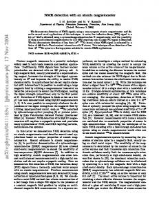
lator is not required, and simpler operation since frequency subtraction is not required. The magnetic sensor, shown in Fig. 1, operates using the single-beam M x technique8,9 to determine the Larmor frequency, which achieves maximum sensitivity when the static magnetic field is oriented at 45° with respect to the sensor’s optical axis. In classical terms, a circularly polarized laser beam tuned to the D1 transition passes through a vapor cell containing 87Rb atoms and optically pumps the atomic spins along the propagation direction of the light. The spins then precess around the magnetic field but with random phase. A radio frequency 共rf兲 magnetic field is applied at the Larmor frequency parallel to the optical axis. The corotating component of the rf field coherently drives the magnetic resonance, making the atomic spins precess in phase and thereby modulating the intensity of the transmitted light. The amplitude and phase of the resonant response of the atoms give a measure of the Larmor frequency and thus the magnetic field. The magnetic sensor is constructed by stacking the various components on a fused silica baseplate with patterned gold electrodes to bring electrical signals to and from the
FIG. 1. 共Color online兲 Chip-scale atomic magnetometer. 共a兲 Schematic of the magnetic sensor. The components are 共1兲 VCSEL; 共2兲 polyimide spacer; 共3兲 optics package including 共from bottom to top兲 a neutral-density filter, polarizer, a quartz quarter wave plate, and a neutral-density filter; 共4兲 ITO heater; 共5兲 87Rb vapor cell with rf coils above and below it; and 共6兲 ITO heater and photodiode assembly. 共b兲 Photograph of the magnetic sensor. Note the gold wire bonds providing the electrical connections from the baseplate to the device.
0003-6951/2007/90共8兲/081102/3/$23.00 90, 081102-1 Downloaded 26 Feb 2007 to 132.163.11.84. Redistribution subject to AIP license or copyright, see http://apl.aip.org/apl/copyright.jsp
081102-2
Schwindt et al.
FIG. 2. 共Color online兲 共a兲 Photograph and 共b兲 schematic side view of the ITO heater. Two glass substrates with patterned ITO are glued together with a nonconductive epoxy to make a heater with reduced magnetic fields. The lighter color lines in the heater are where ITO has been removed through laser patterning. After the ITO patterning, gold pads are deposited for wire bonding, and a 2 m insulating layer of benzocyclobutene is deposited over the remaining exposed ITO so that electrical contact between the upper and lower ITO layers is made only through the gold pads. The large arrows show where the current enters and exits the heater. The electrically conductive epoxy provides the connection between the upper and lower ITO.
device 共Fig. 1兲. Laser light at 795 nm is derived from a vertical-cavity surface-emitting laser 共VCSEL兲. The VCSEL is placed on the baseplate over a patterned resistive element, which dissipates 7 mW to heat the laser and tunes the laser wavelength to the atom’s optical resonance. Before entering the alkali vapor cell, the laser light passes through several optical elements that create circular polarization and attenuate the light to ⬃10 W. A linear polarizer is included to reject an unwanted laser mode orthogonal to the dominant mode and to ensure that the linear polarization of the light is well aligned to the quarter wave plate. Next in the stack is the alkali vapor cell, where a single-turn coil and an indiumtin-oxide 共ITO兲 heater are placed both above and below the cell. The microfabricated Rb vapor cell is constructed by anodic bonding of two glass wafers to each side of a 1 mm thick silicon wafer that has been etched to form a hermetically sealed 1 ⫻ 2 ⫻ 1 mm3 cavity.10 Before the final sealing, the cell was filled with 87Rb and 270 kPa of N2 which broadens the optical linewidth to 18 GHz. The ITO heaters dissipate 175 mW of power to heat the cell to 110 ° C to create a sufficient atomic density. The two coils on either side of the cell are formed by patterning gold on a glass wafer and provide the rf magnetic field. At the top of the stack a p-i-n silicon photodiode detects the light transmitted through the vapor cell. The device occupies a volume of ⬃25 mm3 and uses 194 mW of power. Critical to the operation of the magnetometer is the design of the ITO heater. The magnetic field from any current flowing near the vapor cell will be detected by the atoms, so great care is taken to reduce the effect of the heater currents. To largely cancel the magnetic field produced by the ITO heater current, we configure the current to double back on itself. This is achieved by first laser patterning the ITO so that the current flows through a 120 m wide strip of ITO 共Fig. 2兲. The meandering path of the current makes the heater resistance high 共2 k⍀兲, reducing the current, and spreads the power dissipation over the majority of the heater, evenly heating the cell window. To create a return path for the cur-
Appl. Phys. Lett. 90, 081102 共2007兲
rent that is separated by only ⬃10 m from the path of the input current, we glue two patterned ITO heaters together, the second having the mirror image pattern of the first. Thus, the magnetic field created by the current flowing through the lower ITO layer is canceled by the field of the return current flowing directly above it in the upper ITO layer. To further reduce the effects of the ITO heater currents, we use an alternating current through the heater at a frequency ranging from 2 to 10 kHz. By comparing the measured magnetic field when using alternating and direct currents through the heaters, we observe the field produced by the heaters when using direct current to be 23 nT and the broadening of the magnetic resonance to be 110 Hz 共out of a total broadening of 1800 Hz兲. Both the laser heater current and the laser injection current produce additional perturbing magnetic fields. The effect of the laser heater current is easily mitigated by heating with alternating current at the same frequency as the ITO heater current. However, the VCSEL injection current of 5.2 mA cannot be alternated. This current produces an estimated field of 3.5 nT at the cell with a field variation across the cell of approximately 2 nT. When the magnetometer is in operation, the ITO heater current is set to a constant value to provide sufficient atomic absorption. The current from the photodiode is amplified by a transimpedance amplifier and is then sent to two lock-in amplifiers. One lock-in is used to servo the laser frequency to the atomic resonance by controlling the laser temperature. For this lock, the VCSEL current is dithered at 350 Hz. The second lock-in demodulates the M x signal where the rf coil drive frequency is the reference. Capacitive coupling between the ITO heaters and photodiode causes a modulation on the photodiode signal at the heater frequency that is a factor of 7 larger than the M x signal. Therefore, a notch filter is used to suppress the heater frequency in the photodiode signal before it is sent to the lock-in amplifiers, allowing them to operate with higher input gain. The miniature magnetic sensor is tested inside a twolayer cylindrical magnetic shield containing a solenoid, which applies a controlled field parallel to the cylindrical axis. The sensor sits on a 45° mount in the center of the shield. To optimize the sensitivity of the magnetometer, we tune the cell temperature, rf power, and the VCSEL current, which varies the light power. The cell temperature is adjusted to give approximately 25% absorption of the incident light. This is a balance between the increasing signal amplitude as more atoms interact with the light and the increasing linewidth due to more frequent spin-exchange collisions. We find the optimal light and rf power to be those that power broaden the magnetic resonance by roughly a factor of 2, to 1700 Hz 共Fig. 3, inset兲. When the light and rf power are extrapolated to zero power, the linewidth is 900 Hz. Before the cell was integrated into the magnetic sensor, a linewidth of 230 Hz was measured by extrapolating to low temperature, suggesting that most of the broadening is due to spin-exchange collisions, while the remaining broadening is due mainly to the diffusion to the cell walls. The sensitivity of the magnetometer is determined by recording the voltage noise of the in-phase lock-in amplifier output signal and scaling it by its slope due to a change in magnetic field 共Fig. 3, inset兲. The sensitivity is 5.0 pT/ Hz1/2 over the range of 1 – 100 Hz 共Fig. 4兲. At frequencies below 1 Hz, the noise is seen to increase; this is likely due to a drift
Downloaded 26 Feb 2007 to 132.163.11.84. Redistribution subject to AIP license or copyright, see http://apl.aip.org/apl/copyright.jsp
081102-3
Appl. Phys. Lett. 90, 081102 共2007兲
Schwindt et al.
FIG. 3. Response of the magnetometer is plotted as a function of frequency when a chirped 2.4 nT modulation is applied to the 5.5 T static field. Inset: The in-phase lock-in amplifier output as a function of magnetic field where the frequency of the applied rf field is 38.5 kHz.
in the temperature of the vapor cell and a drift in the applied magnetic field. At frequencies above 100 Hz the response of the sensor rolls off 共Fig. 3兲, reducing the slope of the lock-in signal. Over the 1 – 100 Hz range, the sensor operates at a noise level a factor of 2.6 higher than the photon shot noise. The major contributor to the noise is increased photocurrent noise due to the operation of the photodiode near 110 ° C. The bandwidth of the magnetometer is determined by applying a chirped sine wave modulation to the static magnetic field and measuring the response 共Fig. 3兲. The magnetometer behaves roughly as a single-pole low-pass filter with a 3 dB bandwidth of 1.0 kHz. The bandwidth is roughly established by the coherence time of the atomic spins, i.e., the linewidth of the magnetic resonance. This represents a large improvement in the bandwidth over our previous chip-scale magnetometer, which was limited to 20 Hz because the simple ITO heaters used in that device produced too large magnetic field and needed to be chopped on and off at 40 Hz.3 Although an M x magnetometer is nominally a scalar magnetometer, the sensitivity and accuracy of the device are affected by the magnitude and the orientation of the magnetic field. We measured the sensitivity of the device up to 37 T and observed a degradation in the sensitivity by a factor of 3. This is largely due to the photodiode responsivity
FIG. 4. Noise density of the lock-in signal converted to units of magnetic field. The lock-in time constant is 0.1 ms with a filter rolloff 6 dB/octave. The ambient field is 5.5 T.
rolling off at frequencies above 100 kHz. The orientation relative to the magnetic field greatly affects the operation of the magnetometer. The M x magnetometer is not sensitive to magnetic fields parallel or perpendicular to the axis of the device. For most applications an angle near 45° can be easily maintained, or two magnetometers at different orientations can be used.5 Additionally, there are shifts in the magnetic field reading as the device is rotated 共heading errors兲. Sources of heading errors include magnetic fields produced by the sensor itself, misalignment of the rf field to the optical axis, spurious phase shifts in the electronic feedback, and the nonlinear Zeeman effect. While the first three issues can be mitigated through careful design of the device, the nonlinear Zeeman effect produces a more fundamental problem at fields greater than 10 T. However, it can be largely corrected by sending two side-by-side beams of opposite circular polarization through the vapor cell each and detecting the two beams with a single detector.11 Interestingly, our previous chip-scale magnetometer excited a 共hyperfine兲 coherence between states of a single azimuthal quantum number and therefore did not suffer from this heading error. In summary, the use of microfabricated components. The use of the M x technique has allowed nearly an order of magnitude improvement in magnetic field sensitivity over that of our previous microfabricated sensor using a hyperfine resonance. Additionally, the improved ITO heater design has allowed the bandwidth to be increased to 1 kHz. Further improvements in the design of the magnetometer will reduce the power consumption and the heading errors of the device, enabling the use of chip-scale atomic magnetometers in a wide variety of applications. The authors gratefully acknowledge valuable advice from H. G. Robinson, V. Gerginov, Y.-J. Wang, L. Hollberg, M. Prouty, and S. Schima. This work was supported by the US Defense Advanced Research Projects Agency 共DARPA兲 and the Strategic Environmental Research and Development Program 共SERDP兲. This work is a contribution of NIST and is not subject to copyright. 1
S. Knappe, V. Shah, P. D. D. Schwindt, L. Hollberg, J. Kitching, L.-A. Liew, and J. Moreland, Appl. Phys. Lett. 85, 1460 共2004兲; R. Lutwak, J. Deng, W. Riley, M. Varghese, J. Leblanc, G. Tepolt, M. Mescher, D. K. Serkland, K. M. Geib, and G. M. Peake, 36th Annual Precise Time and Time Interval 共PTTI兲 Meeting, Naval Observatory, Washington, DC, 2004, pp. 339–54. 2 M. V. Balabas, D. Budker, J. Kitching, P. D. D. Schwindt, and J. E. Stalnaker, J. Opt. Soc. Am. B 23, 1001 共2006兲; K. F. Zhao and Z. Wu, Appl. Phys. Lett. 89, 261113 共2006兲. 3 P. D. D. Schwindt, S. Knappe, V. Shah, L. Hollberg, J. Kitching, L.-A. Liew, and J. Moreland, Appl. Phys. Lett. 85, 6409 共2004兲. 4 C. D. Hardwick, Geophysics 48, 2024 共1984兲. 5 W. H. Farthing and W. C. Folz, Rev. Sci. Instrum. 38, 1023 共1967兲. 6 In Magnetism in Medicine: A Handbook, 2nd ed., edited by W. Andra and H. Nowak 共Wiley, Berlin, 2007兲. 7 H. G. Dehmelt, Phys. Rev. 105, 1487 共1957兲; 105, 1924 共1957兲. 8 A. L. Bloom, Appl. Opt. 1, 61 共1962兲. 9 S. Groeger, G. Bison, J.-L. Schenker, R. Wynands, and A. Weis, Eur. Phys. J. D 38, 239 共2006兲; E. B. Aleksandrov, M. V. Balabas, A. K. Vershovskii, A. E. Ivanov, N. N. Yakobson, V. L. Velichanskii, and N. V. Senkov, Opt. Spectrosc. 78, 325 共1995兲. 10 L.-A. Liew, S. Knappe, J. Moreland, H. Robinson, L. Hollberg, and J. Kitching, Appl. Phys. Lett. 84, 2694 共2004兲. 11 T. Yabuzaki and T. Ogawa, J. Appl. Phys. 45, 1342 共1974兲.
Downloaded 26 Feb 2007 to 132.163.11.84. Redistribution subject to AIP license or copyright, see http://apl.aip.org/apl/copyright.jsp