Xiang, and Peter G. Schultz, Adv. Mater 9, 1046 (1997). 4. "Discovery of a Novel Blue Photoluminescent Materials Using. Combinatorial Libraries". Jingsong ...
MATERIAI.~ Today
Combinatorial Synthesis and High Throughput Evaluation of Functional MaterialsAn integrated materials chip approach to discovery, optimization and study of advanced materials X.-D. Xiang Introduction
state materials libraries. 3 Another common approach used by many solid state physicists is to generate a compositional spread using off-axis thin film codeposition. Although very effective and exhaustive, this method is limited to ternary systems with two independent variables. In developing our combinatorial multi-layer thin film method of generating spatially addressable materials libraries (IM chips), several aspects are emphasized. First, the method is applicable to materials systems with unlimited numbers of composition variables. Second, mathematical mapping strategies are used to maximize the variation in sample composition (usually in a discrete manner) with minimized fabrication steps, critical for large scale searching of the compositional landscape. Third, the libraries generated are compatible with high throughput screening of various physical and chemical properties. In addition, the environmental benefit (more than six orders of magnitude reduction in chemical waste generation compared to conventional methods has been achieved) and compatibility to the wide range of electronic/photonic application of the materials were also considered.
Functional materials play a key role in science and technology. Materials with interesting properties, ranging from superconductivity, ferroelectricity, colossal magneto-resistivity and electro-optical effects, just to name a few, are crucial to a wide range of applications. Given the large universe of possible compounds that can be formed by mixing different elements from the periodic table, our current knowledge of functional materials is miniscule. The conventional method of synthesizing and testing samples one at a time seems to be an inadequately slow vehicle for exploring the universe of novel materials. Recently, we have demonstrated that, using technologies similar to those used to make and inspect integrated circuit (IC) chips, materials libraries or integrated materials (IM) chips containing large collections of diversely different compounds can be made and screened to accelerate the exploration by a factor of thousands to possibly millions.
Synthetic method
For example, a fractal mapping strategy was used to maximize the efficiency of library fabrication. 4 This quaternary masking scheme uses a series of n masks, which successively subdivide the substrate into a series of self-similar patterns of quadrants as shown in Figure 1. Each mask is used in up to four sequential depositions; each time the mask is rotated by 90*. This process produces 4 n different compositions with only 4n deposition steps and n masks. The power of this strategy increases exponentially with n. It can be used to
There has long been much desire and effort towards accelerating the rate of materials exploration. For example, robotics approaches were used to emulate and replace the human activity of bulk synthesis (in Japan) and solution synthesis (in UK 2) of inorganic compounds in a effort to discover new high T c superconductors. We have also demonstrated that multihead inkject delivery systems can be used to perform automated micro-synthesis of solid
. . . . . . . .
°°°•.J•°
° • ° • ° , , ° ° ° n ° ° • .
.
.
.
.
.
.
.
°,
. . . . . ° • = , u ° ,
.
.
.
.
.
.
.
.
°°•••, °°°°•,•,
,°o°°°°°
°
....
°°°,°°•, .
.
.
.
.
.
.
.
° .
.
.
.
.
.
.
.
.
• .
.
.
.
.
.
,
,
,
°
°
.
.
.
.
.
. .
. .
.
° ,
.
.
.
.
.
.
.
.
.
.
.
,
.
°
=
°
,
=
°
,
°
•
.
,
°
=
•
°
,
°
=
,
.
°
,
°
o
*
,
°
,
,
.
=
°
=
.
,
,
°
°
°
.
°
,
.
° ,
.
.
.
.
° • ° • ° ° ° ° , ° ° • ° u ,
.
A i
.
.
.
.
.
.
Bi
.
.
°°,•°°,
• ° .
.
.
....
• H ,
°°,°
~°•
°°=°
•°°°
•°°,
=°°
Ci
Di
Ei
Fig. 1. Masks for generating the quaternary library." Ai, B i, C i, D i a n d E i represent a deposition step with mask X rotated counterclockwise by (i-l) x 90 ° Page 23
blATERIAI£ Today effectively survey materials consisting of up to n elemental components where each component is selected from a group of (up to four) precursors. The implementation of masking schemes is accomplished using either physical shadow mask ~ or photolithographic lift-off.4 Photolithography, widely used in the fabrication of micro-electronic chips, is well suited for generating oxide materials chips containing a high density of sites due to its high spatial resolution and alignment accuracy. On the surface, this multi-layer thin film synthesis approach seems to be straightforward. However, it was not clear in the earlier stage of our effort that the approach would be able to generate meaningful crystalline compounds. Since the precursors are deposited sequentially as thin film multilayers, nucleation will occur at each interface at elevated temperatures. Therefore, it is very likely that multiple binary phases will be formed instead of the desired multi-element single phase. In fact, we made many failed attempts before an effective synthetic approach was found. This approach takes advantage of competition between interdiffusion and nucleation at the interfaces. There exists a critical thickness (few tens to hundreds of/k for most oxides) for sequential precursor layers. Below this thickness, the interdiffusion process is dominant over the nucleation process at relatively low temperatures. Therefore, it is possible to interdiffuse the precursor layers at a relatively low temperature to form an intermediate amorphous state close in stoichiometry to the desired phase, prior to the nucleation of thermodynamically stable phases. 5 A two-step process has been adopted to synthesize the materials libraries. 1 First, an extended period of low temperature (100 - 400°C) annealing process is used for proper interdiffusion of thin film precursors. Rutherford backscattering (RBS) and x-ray diffraction studies indicate that, after the low temperature diffusion process, the intermediates are in an amorphous state with no crystalline formation and resulting films have the intended and uniformly distributed compositions. In the second step, a high temperature annealing process is used for phase-formation. In this process, multiple identical libraries are often made to undergo different processing conditions, such as annealing temperatures and atmospheres to optimize the crystalline formation. X-ray diffraction studies are used to characterize the crystallinity of the samples. We have demonstrated that this film growth procedure can be used to obtain predominantly single-phase epitaxial films on lattice matched substrates, allowing epitaxial growth of entire integrated materials chips. 6 So far, w e have predominantly used this approach to synthesize oxide materials. However, nitrides and other materials, which are difficult to make by conventional bulk synthesis methods, can also be easily synthesized using this approach.
Page 24
High throughputscreening A key aspect of the combinatorial approach is the ability to rapidly measure a particular materials property of interest. Although detailed physical characterization may require bulk samples, quick screening of a few key properties of samples on the chips is crucial. In general, optical properties and the properties that can be derived from optical measurements are easier to screen. Optical measurement systems are either commercially available or can be easily assembled with commercial available modules. For example, an optical scanning spectrophotometer has been built from commercial modules to evaluate the photon output and chromaticity of each member in phosphor libraries (chips) upon excitation with monochromatic UV light. 4 Several other optical imaging systems have also been developed to measure, e.g. electro-optical coefficient, magneto-optical effect and surface magnetization. However, quick, nondestructive and quantitative characterization of the complex electrical impedance (at microwave frequencies) of materials presents a very challenging task. Characterization of electrical impedance is extremely important for many applications, including superconductivity, ferroelectrics/dielectrics, magnetoresistivty and various semiconductor properties. For example, in the case of frequency agile (tunable) materials applications, three key properties - electric-field tunability (nonlinear dielectric constant), dielectric constant and loss tangent - all need to be characterized at microwave frequencies. Conventional contact measurements using electrodes often yield misleading information due to interfacial effects, in addition to being destructive and posing many difficulties in implementing them on materials libraries. To this end, we have developed a novel scanning evanescent microwave microscope (SEMM) and relevant near-field analytical solutions, which allowed nondestructive and quantitative microscopy of microwave impedance of any materials with unprecedented sensitivity and spatial resolution (100 nm). 7 A theory which calculates evanescent microwave interaction between the tip and sample analytically allows a high resolution microscopy of impedance at the frequencies relevant to most electronic applications. 7 The microscope is routinely used for quantitative characterization of linear and nonlinear dielectric constants of ferroelectrics and dielectrics.6 A low temperature version has also been developed to characterize superconductors.8 Probably the most difficult characterization is structural characterization, which currently still represents a time consuming bottleneck in the combinatorial materials approach. Recently, significant effort has been made to apply the x-ray micro-beam technique available at a number of synchrotron radiation facilities for structural characterization of materials chips. 9
MATERIALS Today
Applications In our earlier efforts, this approach has been used to identify a class of cobalt oxide magnetoresistive materials of the form (La0.88S0.]2)CoO3.1° Previously, large magnetoresistances were found only in Mn-based perovskites. Using materials chips, we searched through V, Cr, Fe, Co, and Ni based perovskites in a very short time period with a discovery of magnetoresistive cobalt oxides. Magnetoresistance was found to increase as the size of the alkaline ion increased, in contrast to Mn-containing compounds, in which the magnetoresistive effect increases as the size of the alkaline earth ion decreases. The technique has been applied to the optimization and discovery of luminescent materials. The systematic search of novel luminescent materials has led to the discovery of a number of rare earth doped refractory metal oxide phosphors including (Gdo.6Sro.4) All. 6 O3+~F1.8:Eu2+o.08(green), Laml3.103+8:Eu2+o.o08(blue) and GdAll.603+~:Eu3+o.08 (red) with photoluminescent quantum efficiencies of approximately 100%, 60% and 100%, respectively, 1] and a red phospor (Gdl.54Zno.46) O3_~:Eu3+0.06, with photoluminescent quantum effiiciency of =,86% and a superior color chromaticity (x=0.656, y=0.344) compared to the state of art red phosphor y203:Eu3+. 12These phosphors also show excellent X-ray and cathodoluminescent properties. More recently, a novel blue emitting luminescent composite material Gd3Ga5012/SiOx, 4 has been discovered using an integrated materials chip shown in Figure 2. As in many important discoveries in materials research, this finding is entirely unexpected. However, the materials library approach has dramatically increased the probability of the serendipitous discovery. The interfacial (between Gd3GasO]2 and SiOx) effect is attributed to efficient blue photo-luminescence in this composite material. The possibility of electroluminescence in this materials, which would enable a wide range of applications, is currently under investigation. This approach has also been recently applied to ferroelectric materials where the effects of transition metal dopants on the dielectric constant and tangent loss of a library of epitaxial thin films of (BaxSrl_x)TiO3 were determined as shown in Figure 3. 6 In particular, addition of 1 mol% W was found to reduce the high frequency (MHz and GHz) loss tangent by more than four fold. This finding is especially important for microwave application of these tunable dielectric materials.
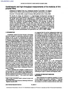
,x 0 1 2 3 4 5 6 7 8 910111213141516171819202122232425262728293031
0 I 2 3 4 5 6 7 8 9 10 11 12 13 14 15 16 17 18 19 20 21 22 23 24 25 26 27 28 29 3O 31
0 1 2 3 4 5 6 7 8 9 10 11 12 13 14 15 16 17 18 19 20 21 22 23 24 25 26 27 28 29 30 31 o 1 2 3 4 5 8 7 8 910111213141516171819202122232425262728293031
Fig. 2. (a) Photograph of the as-deposited quaternary library under daylight. The diversity of colors in the different sites stems from variations in film thicknesses and the optical indices of refraction; The five masks A, B, C, D and E (illustrated in Fig. 1) were used to generate the libraries. The sequence of masking and precursor deposition is: A]: Gae03 (355 nm), Az: Gae03 (426 nm), A3: SiOe (200 nm), A 4" SiO 2 (400 nm), 01: CeO 2 (3.5 nm), De: EuF3 (11.3 nm), D3: Tb407 (9.2 nm), El: Ag (3.8 nm), Ee: TiOe (6.9 nm), E3: Mn304 (5.8 nm), BI: Gd20 3 (577 nm), Be: ZnO (105 nm), B3: ZnO (210 nm), CI: Gd203 (359 nm), C2:Ye03 (330 nm), and C~: Ye03 (82.5 nm), where the numbers in the parentheses are the thickness of the deposited films. (b) Luminescent photograph of the processed quaternary library under irradiation from a multiband emission UV lamp at short wavelength (centered around 254 nm). Page 25
~ T E R I A I ~ Today 6
tanb -.o.s0 -,0.40 --0.~ -0.20 "0.10
2
3
(!)
~
"O.O6
Fig.3.(a) Dielectric constant (er) and (b) loss tangent (tan 6) of doped BaTi03 films on LaAI03. To fabricate the library, Ti02 (870 A) was deposited first to generate an array of 256 samples, each 650 Itm x 650 pro, on a single crystal (001) LaAl03 substrate. This was then followed by deposition of BaF2, SrF2 and different dopants in the following sequence using the masks illustrated in Fig.l: C2:Fe203 (7 A);CI: W (5 A); C4:CaF2 (12 A); D2: Cr (4 A); DI: Mn304 (7 A); D4: Ce02 (12 A); E2: MgO (7 ft); E;: Y203 (10 A); E4: La203 (12,4); Be." BaF2 (1640 A); Bt." SrFe (270.4)+BaF2 (1320 A); B4: SrF2 (410 ,~)+BaF2 (940 ,~); B3: SrF2 (680 ]t)+BaF2 (830 A).
Future outlook T h e w o r k described above is only the beginning o f a revolution in materials research. N e w synthetic techniques and high throughput screening systems will be invented as m o r e scientists j o i n the game. If w e stretch our imagination, m a n y possibilities are within our reach. Countless materials p r o b l e m s that are important to industry applications, such as e f f e c t i v e d i f f u s i o n barrier for c o p p e r or silver interconnects, can be efficiently addressed using this approach. With rapid d e v e l o p m e n t o f technology, this and similar approaches m a y b e c o m e c o m m o n practice in the materials research o f the next century.
7.
8.
9.
10.
References 11. 1. "A Combinatorial Approach to Materials Discovery" X.-D. Xiang, Xiaodong Sun, Gabriel Briceno, Yulin Lou, Kal-An Wang, Hauyee Chang, William Gregory WallaceFreedman, Sung-Wei Chen, Peter G. Schultz, Science 268, 1738-1740 (1995). 2. "The Search for New Superconductors" S.R. Hall and M. R. Harrison, Chemistryin Britain 739, (Sept. 1994). 3. "Solution-Phase Synthesis of Materials Libraries" Xiao-DOng Sun, Kai-An Wang, Young Yoo, William G. WallaceFreedman, Chen Gao, X-D. Xiang, and Peter G. Schultz, Adv. Mater 9, 1046 (1997). 4. "Discovery of a Novel Blue Photoluminescent Materials Using Combinatorial Libraries" Jingsong Wang, Young Yoo, Chen Gao, Ichiro Takeuchi, Xiaodong Sun, X-D. Xiang, Peter G. Schultz, Science 279, 1712 (1998). 5. Fister, T. Novet, C.A. Grant, D.C. Johnson Adv. in Synthesisand Reactivity of Solids2, 155 (1994). 6. "Combinatorial Synthesis and High Throughput Evaluation of Ferroelectric/Dielectric Thin Film Libraries for Microwave Applications"
Page 26
12.
H. Chang, C. Gao, I Takeuchi, Y. Yoo, J. Wang, P. G. Schultz, and X.-D. Xiang, R. E Sharma, M. Downes, and T. Venkatesan, AppliedPhysicsLett. 72, 2185 (1998). "High Spatial Resolution Quantitative Microwave Impedance Microscopy by a Scanning Tip Microwave Near-Field Microscope" Chen Gao, Tan Wei, Fred Duewer, and X-D. Xiang, Applied PhysicsLett. 71, 1817 (1997). "Sub-micron Resolution Imaging of Complex Microwave Impedance of YBazCu30 XPatterned Thin Films at Variable Temperatures" Ichiro Takeuchi, Fred Duewer, and X.-D. Xiang, AppliedPhysicsLetters. 71, 2026 (1997). "Synchrotron X-ray Microbeam Diagnostics of Combinatorial Materials Libraries" E. D. Issacs, M. Kao, G. Aeppli, X.-D. Xiang, X.Sun, E Schultz, M.A. Marcus, G. S. Cargill, and R. Hanshalter, AppliedPhysics Letters (in press). "Discovery of a Class of Cobalt Oxide Magnetoresistance Materials Using Combinatorial Synthesis" Gabriel Briceno, Hauyee Chang, Xiaodong Sun, Peter G. Schultz, and X.-D. Xiang, Science 270, 273 (1995). "Identification and Optimization of Advanced Phosphors Using Combinatorial Libraries" Xiao-Dong Sun, Chen Gao, Jinsong Wang, and X.-D. Xiang, AppliedPhysicsLett., 70 (June 23, 1997). "New Phosphors (Ga2-xZnx)O3-d: Eu3+ with High Luminescence Efficiency and Superior Chromaticity" Xiao-Dong Sun and X.-D. Xiang, AppliedPhysicsLett. 72, 525 (1998).
Acknowledgement I would like to acknowledge the important contributions from my colleagues at Laurence Berkeley National Laboratory, Drs. Peter G. Schultz, Chen Gao, Ichiro Takeuchi, Kai-An Wang, Tao Wei, Gabriel Briceno, Jingsong Wang, Yulin Lou, also Hauyee Chang, Sung-Wei Chen, W. G. Wallace-Fredman and Young Yoo to this project. This work was supported by the Director of Advanced Energy Projects Division, Office of Computational and Technology Research, U.S. Department of Energy under contract DE-AC03-76SF00098 and the Office of Naval Research, Order No. N00014-95-F-0099.