Jul 29, 1993 - Because R2C2 = R,C,, the delay between point c and d is equal to that between c and a. Hence, the skew between U and d is ideally zero as ...
[6]. The unknown equivalent electric current on the dipole surface
and 6.25, for the H E M , , mode. Summary: A numerical design tool has been used to design a halfsplit CDR antenna excited by a coaxial prohe which promises improved bandwidth, radiation efficiency, and power handling capabilities as compared to conventional microstrip and slot-coupled transmission line antennas. Although results were presented only for the TEo, and HEM,, modes, other quasi-TE modes can be excited using this configuration. Acknowledgments: This work was partially supported by the
National Science Foundation under grant number ECS-9015328. 0 IEE 1993
29 July 1993
Electronics Letters Online No: 19931215
-2ot . ’ . ’ 17 18 19
’
8
’
’
.
20 21 frequency, GH z
a
’
.
22
I
G. P. Junker, A. A. Kishk and A. W. Glisson (Departmenr of Electrical Engineering, University of Mississippi. MS 38677, USA)
2 3
1916131 References 1
JUNKER, G P , KISHK. A A . ,
and GLISSON. A W.: ‘MOM solution of wire
radiators coupled to dielectric bodies of revolution’, IEEE Antennas and Propagat. Society h i . Symp. Dig., 1993,1, pp. U 3 2 GLISSON, A.W , and BUTLER, C.M : ‘Analysis of a wire antenna in the presence of a body of revolution’, IEEE Trans., 1980, AP-28, pp. 604487 3 SCHAEFFER. J F , and MEDGYESI-MITSHANG, L N.: ‘Radiation form wire antennas attaches to bodies of revolution: the junction problem’, IEEE Trans., 1981, AP-29, pp. 479487 4 MONGIA, R K , ITTIPIBOON. A , ANTAR. Y M M , BHARTIA, P, and
-151 2 4 b
’
1
2.6
20
3.0
frequency. GHz
,..
”
’
’
’
CUHACI. M : ‘A half-split cylindrical dielectric resonator antenna using slot-coupling’, IEEE Microw. & Guided Wave Lett., 1993, 3, pp. 38-39 5 KAJFEZ, D., and GUILLON, P., (Eds.): ‘Dielectric resonators’ (Artech House, Inc., Norwood, MA, 1986) 6 KISHK. A A , and SHAFAI. L : ‘Different formulations for numerical solution of single and multihodies of revolution with mixed boundarv conditions’, IEEE Trans.. 1986. AP-34. Dn. 666-673 7 HARRINGTON, R F.: ‘Time harmonic electromagnetic fields’ (McGraw Hill, New York, 1961)
3-4
3 2
1936/31
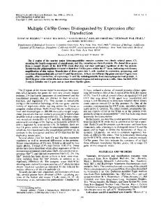
Fig. 3 Input impedances for half-split CDRA E, = 8.9, h = 3.0cm, a = 2.25cm, a, = 0.0118cm a TEol mode with xt = 1.6cm, z, = O.Ocm, and 1, = 1.25cm b HEM,, mode with x, = z, = O.Ocm, and I, = 0.838cm
Computing centroids in current-mode technique
is modelled as piecewise linear subdomain functions [3]. After application of a Galerkin procedure to the integral equations, the resulting MOM matrix is solved for the current distribution on the wire and the input impedance is computed from the current at the driving source. Other parameters such as the radiation pattern and the near field distribution can also be obtained.
M. Tartagni and P. Perona Indexing terms: Circuit design, Analogue computer circuits A novel current-mode circuit for calculating the centre of mass of a discrete distribution of currents IS described. It is simple and compact, an ideal building block for VLSI analogue IC design. The design principles are presented as well as the simulated behaviour of a one-dimensional implementation.
Numerical results: Excitation of the TEo, mode of the antenna of
Fig. 1 will result in a broadside radiation pattem. This broadside radiation pattem is similar to the radiation pattern of a narrow slot in a ground plane. Excitation of the HEM,, mode results in a radiation pattern with a null along the y-axis. The radiation patterns for the TEol and HEM,, modes for the split cylindrical dielectric disc of Fig. l with a = 2.25cm, h = 3.0cm and E, = 8.9 are plotted in Fig. 2u and b, respectively. A monopole of radius a , = 0.0118cm and length l, = 1.25 and positioned at xf = 1.6an, z, = 0.0 was used to excite the TEo, mode. The input impedance of this mode is plotted as a function of frequency and is shown in Fig. 3a. To assure the convergence of the numerical solution, azimuthal modes from -2 to +2 are included in this analysis. The impedance level can he controlled by adjusting the length and position of the dipole. To properly excite the hybrid H E M , , mode, the prohe length and position were adjusted to l, = 0.838cm and x, = zf = 0. in this position, only the e1 azimuthal modes are excited. The input impedance. is plotted as a function of frequency in Fig. 3b.
Introduction: The idea of using resistive sheet or grids of linear resistors to determine the position of objects, a small bright spot for example, is not new and has been used in earlier systems [l]. More complex analogue VLSI chips have also been proposed to find the centroid and higher-order moments [2].Analogue designs overcome the problem, critical for real-time system operation, of the significant AID conversion overhead required by digital systems. However, a number of difficulties remain:
(i) so far, linear resistive sheet implementations require either complex area-expensive circuitry, or technology-dependent solutions that are not electronically tunable;
The computed resonance frequencies and the radiation Q factors were computed in the complex plane without excitation and are, respectively, 2.033GHz and 7.7 for the TE,, and 3.021GHz
ELECTRONICS LETTERS
74th October 7993
Vol. 29
(ii) the computation of the centroid often requires off-chip processing using sophisticated buffers; (iii) they do not work well for very low levels of injected current, thus preventing direct interface of photodiodes with resistive grids for low light levels.
No. 21
181 1
The above-mentioned problems led us to investigate a new circuit technique using a current-mode approach [3]. This Letter presents a novel CMOS circuit using a current-mode subthreshold MOS approach [4] that is simple, requires little area, does not require off-chip processing, works well with small currents and has low power consumption.
/
n
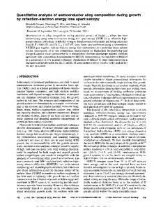
Circuit description. The well known idea underlying our positionsensitive device is described in Fig. la. For a discrete I-D resistive network it may be proved that the relative position slL of current injection is related to the boundary currents I,, I2and voltages VI, Vz by the following expression:
where n and m are the number of elements on the left- and righthand sides of the injection node, R is the single-element resistance value and L is the half-length of the structure as illustrated in Fig. la. It can be seen from the above equation that if V , = Vz the position may be calculated by means of a simple fractional function of the output currents independently of the value of the node voltages. However, owing to the intrinsic differences of device characteristics, a sufficiently accurate matching of the boundary voltages is difficult to achieve, making the position estimation through the function (Z, - Ij)/(I, + I,)accurate only for high values of R andlor I. Thus the requirement to keep R high is extremely important for low values of injected current, but hard to meet in VLSI by using either passive layers or complex circuit strategies. To overcome this limitation we propose the solution described in Fig. lh, where each resistor has been substituted by an MOS transistor. Assuming the general current expression of an MOS transistor ID= K cf( V,, V,) - f( V,, V J ) it i s easy to show that IC --
Fig. 2 Computational circuit
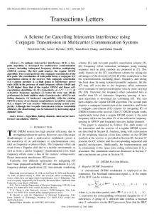
Circuit rvu2uution.- The proposed architecture has been simulated by using ANALOG [6] which is particularly tailored for evaluating MOSFET circuits working in mixed operating regions. A 13node current divider, along with the proposed computational block, has been simulated with typical parameters of a generalpurpose 2 p CMOS process. All transistors have the same size WIL = 4pd4p.m to ensure maximum compactness to the structure. In Fig. 3 the output current is plotted against the centre of
-
-1
0
a -30
~ - m Iz-Ii + % ~ ( f ( I c . ~ 2 j - f ( l . G . I i ) j --~
L-m+m
12+Ii
in + In)'
-50
121 where K i s the channel width to length ratio. Note that the current division technique i s valid in all operating regions of an MOS transistor: weak and strong inversion, linear region and saturation as recently reported also in [5]. For example, referring all voltages to bulk, the value of f( V,, V p ) for PMOS transistors working in K weak or strong inversion i s Ioexp(-KV,+V~U,) or ~ C , J ~(K(-V~, + V,) + V J 2 , respectively, where V, could be either VDor VSrK is the gate effectiveness coefficient, related to the body effect, and U , is the thermal voltage. Furthermore, note that eqn. 2 i s still consistent for MOSFETs in moderate inversion, whatever is the expression o f f ( VG, Vp). This implementation offers the capability of controlling the voltage-dependent term of eqn. 2 simply by adjusting the level of V,, thus determining the resistivity of the network, which trades off time response for boundary offset cancellation. It is easy to see that for both networks, in the presence of multiple inputs and assuming V , = V,, the output currents encode the normalised first moment .aL of the current distribution:
In order to calculate the (I, - 1,)/(12 + I]) function we propose using the translinear principle in a circuit with subthreshold MOSFETs (Fig. 2). Two current-controlled current conveyors consisting of the two pairs MO-M1 and M10-M11 ensure equal
1812
magnitude to V , and Vl while the currents flowing out of the resistive network are delwered at the drain of M5 and M6, avoiding any current-mirror mismatch. Applying the translinear principle to the loop of M 3 , M4, M5 and M6 we can prove that IDiI,, = I,, ID,; hence I,, = Ih(12- 1,)/(12+ 11), giving the required function normalised to the biasing current of the differential pair I,. Finally. note how the above approach and the current-division technique are not directly constrained by power supply margins, an attractive feature for low-voltage applications.
-5
-4
-3
-2
-1
0
1
2
,
3
centroid position
G
5
:03217
Fig. 3 Steadj-state povition charucteristi~5 V , = 2 88V, V: = 2 38V, V, = 0 6 V C, = 0 747V
0. U lOnA
0,. IOpA
mass position of the input distribution assuming a 50mV offset between V , and V.. The circle marked characteristics belong to a three-current pattern whose centroid corresponds to the indicated node while the square marked characteristic i s related to a fourcurrent pattern whose centre of mass is aligned to an internode position. The circuit has been simulated for different values of V,, in the range 1.354.4V (voltages referred to ground) to evaluate the current division performance for different transistor operating regions and to analyse the offset cancellation effect as predicted by eqn. 2. Note that the linearity of the characteristic is not affected by the transistor working region, and that the offset effect gradually decreases for increasing values of V,. For all characteristics we have observed high linearity with correlation coefficient deviation below 0.01%. Fixing Vc,in the range 1.54.4V, we then vaned the total amount of input current over three decades, from 2Opki (solid markers) to 2 0 n N (open markers), obtaining a small variation ( ~ 1 . 5 % )of static characteristics. The lower limit is set by the leakage currents of diffusions and the upper one by the strong
ELECTRONICS LElTERS
14th October 1993
Vol. 29
No. 21
inversion operation of the computational block transistors. Conclusions: W have investigated a new technique for locating in analogue fashion the centre of mass of a discrete distribution of currents using current-mode concepts. The simulation results presented above, which exhibit high linear characteristics over three decades of input values, indicate that this architecture has application versatility in the design of position-sensitive devices (PSD), D/ A conversion systems and neural networks. Analysis of similar architectures in BiCMOS technology is currently in progress to overcome time-response requirements.
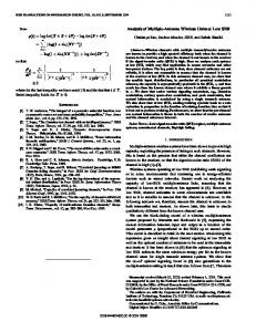
elements (FEs). The clock distribution within each FE is assumed to be locally optimised. The global skew is minimised by compensating for the differences in the phase delays [see note I] of the different FEs through parameterising each of the FE‘S clock buffers in the central clock buffer. This skew minimisation technique is inherently susceptible to drift in the transistor characteristics brought on by process and environmental variations. external clock
LPF
Acknowledgments: We are grateful to C. Mead, R. Sarpeshkar, K.
alb
Boahen and G. Baccarani for their very valuable feedback.
C
-.1
d LL:=L: zL
0 IEE 1993
5 August 1993 Electronics Letters Online No: 19931188 M. Tartagni (DEIS, Universita di Bologna, Viale Risorgimento 2, 40136 BO, Italy) P. Perona (California Institute of Technology, 116-81, Pasadena, CA 91125. USA)
‘Design and perf0r“Ce Of the mesh-type high-speed optical position~sensitivedevices (MEPSDs)’, IEEE Trans., 1991, ED-38, (3), pp. 498-504 IC with 2 STANDLEY, D.L.: ‘ ~ object 0 position and emhedded imape’. IEEE J- . -Solid s t a t p Circuits. 1991. sc-26. 112). ..~.__._ .. . ...\--,, DD. 1853-1859 3 TOUMAZOU, c., LIDGEY, F., and HAIGH. D. (Ed.): ‘Analogue IC design: the current mode approach’ (Peter Peregrinus, 1990) DLTTA,A.K.,
and
HATANAKA Y:
--.----
. I
4
i
L, L,, the delay between c and b will be greater than that between c and d; hence, the clock at d leads the clock at a as shown in Fig. 1. This implies that the skew achieved is negative, which is an interesting result. The opposite case is also illustrated in Fig. 1. This approach can be used to tune the intra-element delay, an effect achieved by the individual sizing of buffers in the Friedman-Powell scheme [4]. Fig. 2 illustrates this application. Let us assume that
Indexing terms: Clocks, Phase-locked loops
A technique for minimising clock skew in VLSI chips and multichip modules is proposed. A phase-locked loop is used to
tune the delay of the clock interconnects. Negative, zero and positive delays can he achieved. This allows for clock synchronisation between individual modules with locally optimised clock distribution to minimise global clock-skew. e2 er
Introduction: The throughput of synchronous processors can be
enhanced by reducing the clock Cycle time [I]. The cycle time can be reduced by decreasing the delays of flipflops and logic blocks in the signal path. This has been achieved by scaling down the device feature size and through other technological breakthroughs. The remaining factor which has not been given enough attention until recently, is the skew time. The skew time must be within 10% of the cycle time [2] to prevent race conditions. Several strategies which have been proposed to minimise clock skew revolve around RC balancing techniques (e.g. H-tree [3]). These techniques, however, are unsuitable for asymmetric distribution of synchronous elements and become complex when used recursively for clock synchronisation on larger chips. A skew reduction strategy which lends itself particularly well to the hierarchical nature of VLSI design is the Friedman-Powell scheme [4]. In this scheme, the master clock source is first buffered to drive the central clock buffers. Parallel connections carry the clock signal from the centralised clock buffer to each of the functional
ELECTRONICS LElTERS
14th October 1993
-
-PY=
I
Fig. 2 Compensation o/phase delay of FEs using PLL-controlled intraelement interconnects
the phase delays of functional elements FE, and FE, are tFm and 1 , respectively, with tFEl< 1,. To avoid skewing between e, and e>, the delay of the first interconnect ( a to d,) should be larger than that of the second interconnect (a to dz). This requirement contradicts the fact the length of the fust interconnect is shorter than that of the second. However, using negative skewing by proper positioning of the remote VCO, the clock at d2 may be made to lead the reference a by f , and the clock at d, to lag the reference by t , . The net result of this arrangement is that the clock at d, lags the clock at d2 by f , , , which is equal to t , + f,. If t , , eauals 1,-t,,. the skew between e , and e, is zero. The condition Note 1: The phase delay is the maximum delay between the master clock source and any leaf node
Vo11. 29
No. 21
1813