Continuous representation of the performance of a CMOS library B. Lasbouygues , J. Schindler , S. Engels , P. Maurine3, N. Azémard3, D. Auvergne3 1
1
2
2
2
ISIM, Université de Montpellier II, Place E. Bataillon, 34095 Montpellier France
STMicroelectronics Design Department 850 rue J. Monnet, 38926, Crolles, France
3
LIRMM, UMR CNRS/Université de Montpellier II, (C5506),161 rue Ada, 34392 Montpellier, France pmaurine, azemard,
[email protected] It is well recognized that the transition time and the Abstract: propagation delay exhibit a nonlinear variation with In a standard industrial approach the timing performance respect to the control and loading conditions. This verification is obtained using a tabular method that necessitates a great amount of simulations. They must imposes variable simulation steps because specify, for each drive in each logic family: the load, the interpolating in this range may induce significant input slope, the temperature and the supply voltage errors. Usually the largest error occurs for the smallest sensitivity, for each edge, of the transition time and values of the load and the input transition time. It is propagation delay. Extending a logical effort like based clear that the relative accuracy, obtained with a tabular model of timing performance of CMOS structures we show method, is strongly dependent on the granularity of the in this paper that it is possible to define a specific table that is not necessarily constant but must cover a performance representation allowing a continuous significant part of the design range. For that, representation of the performance sensitivity of a complete indications for defining the granularity and the family. We describe the parameter calibration procedure and coverage of the design space must be available. validate the proposed representation on a 0.13µm process by In this paper we propose a continuous representation comparing the performance sensitivity deduced from this of the timing performance of a CMOS library. This representation to sensitivity values obtained from electrical simulations performed with the full process model of the representation defines the propagation delay time and foundry. output transition time sensitivities of the cells to the design space parameters, such as the load, the input 1. Introduction transition time, the supply voltage and the temperature values. The performance model is presented in part 2. The complete characterization of the timing In part 3 we detail the calibration method to be used performance of a library involves a huge number of on a specific process. Application is given in part 4 to simulations. The performance of each gate on a path, a 0.13µm STM process, before to conclude in part 5. for each loading and control condition, is obtained from an interpolation between a set of predefined values. These values are determined from electrical simulations performed for a limited number of design conditions, such as load, input transition time, supply voltage value and operating temperature [1]. Characterizing each edge of the transition time and the propagation delay of each library cell, for typically five loading and input ramp conditions, involves 100 simulations. Then considering the process corners, with different supply voltage and temperature values imposes to simulate thousand of points to characterize a logic function designed with different drives. This huge number of simulations just allows to represent the design space with few loading and control conditions. Intermediate conditions must then be interpolated using a linear characteristic equation (Synopsys) : f(τIN,CL)=AτIN+BCL+CτINCL+D).
2 . Model 2.1 Gate switching delay An accurate delay model must be input slope dependent and must distinguish between falling and rising signals. Considering the input-to-output coupling effect [2], the input slope effect can be introduced in the propagation delay as: 2C M vTN τ I NLH (i − 1) + (1 + ) t HLstep (i) C M + CL 2 . (1) 2C M vTP τ I NHL (i − 1) + (1 + ) t LHstep (i) t LH (i) = CM + CL 2 t HL (i) =
τINHL,LH is the duration time of the input signal, generated by the controlling gate, CM the coupling capacitance between the input and output nodes [3], that can be evaluated or directly calibrated from SPICE simulation. Indexes (i), (i-1) refers to the location of the cell in the array.
2.2 Inverter transition time. The output transition time (defining the input transition time of the following cell) of a CMOS structure [4] can be obtained from the modeling of the charging (discharging) current that flows during the switching process of the structure and from the amount of charge (CL.VDD) to be exchanged with the output node as: C ⋅V τoutHL = L DD I NMax . (2) C L ⋅ VDD τoutLH = I PMax CL is the output load and VDD the supply voltage value. In (2) the output voltage variation has been supposed linear and the driving element considered as a constant current generator delivering the maximum current available in the structure. To evaluate the maximum current available in the structure two controlling conditions must be considered, the fast and slow input control ranges. In the fast input range the switching current exhibits a constant and maximum value: Fast I MAX = K N,P ⋅ W N, P ⋅ (VDD − VTN,P ) (3)
obtained for deep submicron from the Sakurai’s representation [5] with α=1. Here KN,P is an equivalent conduction coefficient to be calibrated on the process. From (2,3) we obtain the expression of the transition time for a fast input control condition as: C Fast τoutHL = τ ⋅ (1 + k ) ⋅ L CIN (4) (1 + k) C Fast τoutLH = τ⋅ ⋅R⋅ L k C IN (4) represents an extension of the logical effort model [6] for non symmetrical inverters. τ is a unit delay characterizing the process, k=WP/WN the inverter configuration ratio and R the speed ratio between electron and holes. In the slow input range the input and output voltages vary simultaneously. The resulting short circuit between N and P transistors decreases the current value available at the output. Considering the symmetry property of the current wave shape, this new value of the maximum current available can easily be obtained as: I Slow MAX =
2 K N, P ⋅ WN, P ⋅ VDD ⋅ CL
.
(5)
IN HL , LH
Developing (2) with (5) and (4) gives for a falling output edge: τSlow outHL =
(VDD − VTN ) ⋅ VDD
Fast τoutHL ⋅ τ INLH
(6)
with an equivalent expression for a rising edge. As shown in (4), for a well-defined inverter structure, in the Fast input range, the output transition time only
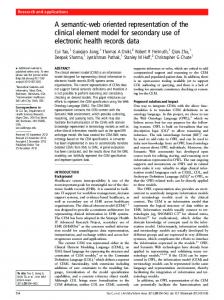
depends on the ratio load/ inverter input capacitance. In the Slow range, the output transition time exhibits an extra input duration time dependency that reflects the complete inter-stage interaction in an array of inverters or gates. This is illustrated in Fig.1 where we represent the transition time for output falling and rising edges, for different values of the configuration ratio, versus the input transition time value τIN. As shown the values of the transition time, calculated from the maximum value of (4) and (6), are in good agreement with the simulated one. τOUTHL (ps )
600 400 200 000 800 600 400 200
Simulation Calculation
k=2
k=1
τIN /t HLS 0
τOUTLH (ps) 1500 1300 1100 900 700 500 300 100
4
8
12
16
Simulation Calculation
20 k=2
k=1
τIN /t LHS 0
4
8
12
16
20
Fig.1. Illustration of the output transition time sensibility to the input transition time τIN.
2.3 Extension to gates. It is obtained [6] by reducing each gate to an equivalent inverter. The current available from the N (P) parallel array of transistors is evaluated as the maximum current of an inverter with identically sized transistors. The array of N (P) series-connected transistors is modeled as an input voltage controlled current generator with a current capability reduced by a factor DWHL,LH. This reduction factor (DW) is defined as the ratio of the current available in an inverter to that of a seriesconnected array of transistors of identical size. I Fast ,Slow (Inv) W (Inv) N, P N, P DW Fast, Slow = ⋅ (7) Fast ,Slow HL, LH W I (Gate) N, P (Gate) N, P
DW corresponds to the explicit form of the logical effort [6]. Note that depending on the input range and on the rank of the controlled input, for a given gate, it may have different values.. Considering eq.7, the output transition time of a gate is easily obtained under the generic expression of [6] as: Fast ,Slow Fast ,Slow τoutHL = τ Fast ,Slow (Inv) ⋅ DWHL HL (8) Fast ,Slow Fast ,Slow τoutLH = τ Fast ,Slow (Inv) ⋅ DWLH LH
2.4 Supply voltage sensitivity. As shown in (4), τ represents the output transition time of an ideal inverter (without parasitic capacitance) designed with
identical transistors and loaded by an identical one. Developing (4) from (2) and (3) gives: Cox ⋅ L VDD τ= ⋅ K N VDD − VTN (9) K N VDD − VTN R= ⋅ K P VDD − VTP Eq.9 gives the supply voltage sensitivity of the transition time and of the propagation delay (1).
This is illustrated in Fig.2 where we represent, using FAST τOUT as a reference, the output transition time variations for the complete family of inverters of a 0.25µm library. As expected all the curves pile up on the same one, representing the output transition time sensitivity to the input transition time. The final value for each specific cell is then directly obtained from the FAST evaluation of τOUT , in (4), that contains the structure and load dependency.
2.5 Temperature sensitivity. Can be included in the model considering both the mobility and the threshold voltage variations described in [7,8]: XT
θ K θ = K nom ⋅ nom . (10) θ VT (θ) = VTnom − δ(θ − θ nom ) K and VT are respectively the conductivity factor and the threshold voltage, Θnom, Θ, represent the reference and the targeted temperature, XT and δ are the temperature coefficients of the mobility and threshold voltage. Coupling (9) and (10) a general expression for the τ supply voltage and temperature sensitivity can be obtained: τ( VDD , θ) θ = τ nom θnom
XT
VDD 1 ⋅ − V V V Tnom + δ(θ − θnom) DDnom DD VDDnom − VTnom
(11) The different parameters of (11) can directly be determined from specific simulation conditions that we will define in the next part. 3. Continuous representation and Calibration 3. 1 Uniform representation. Let us now consider the case of rising edges applied to the input of gates. As it can be deduced from (4,6,8), in the Fast input range, FAST τOUT is characteristic of the inverter structure (gate) and of its load. Considering the sensitivity of the FAST different expressions to the input slope, τOUT can be used as an internal reference of the output transition time of the considered structure. In this condition we can write: 1 τoutHL τ INLH (12) VDD − VTN = ( Inv ) Max ⋅ Fast τ Fast VDD τ outHL outHL Normalizing the output transition time with respect to τoutHLFast, used as a reference, the resulting expression only depends on the input transition time. It is configuration ratio and load independent. Similar results are obtained for gates and the representation of propagation delay.
Fig.2. Full representation of the output transition time variation of the 7 inverters of a 0.25µm library.
3.2 Parameter extraction method. As shown in Fig.2 and (1,8,12) it appears that the output transition time and the propagation delay of all the gates of a library can be characterized with a reduced set of electrical simulations. a) The τ value is obtained from the output transition τHL (falling edge) of an heavily loaded inverter (with a known configuration ratio k) controlled by a fast input ramp (τIN< τOUT). b) R is obtained from the ratio τLH/τHL. c) For small load the variation of the apparent τ value determines the value of Cpar and CM. d) In the slow input range (τIN> τOUT), varying τIN determines the input slope sensitivity (6). e) Using the inverter as a reference the parameters k and DW are determined from τGate/τInv. f) Eq.9 determines the supply voltage sensitivity. g) The temperature parameters, XT and δ are obtained from the preceding steps realized at different temperature values. 4. Application to a 0.13µm library We have applied this method to a 0.13µm library from STM. In this work we just considered the simple gates, an Inverter with 7 different drives, a Nand and a Nor with two and three inputs and 5 different drives. Initially the timing performance (transition time and propagation delay) of all these elements has been characterized from electrical simulations. They are available in tables (TLF, STF) that give, for each edge of the transition time and the propagation delay of each element, for 3 temperature and supply voltage values, the corresponding performance for 5 different values of the load and the input transition time.
We have determined on the different tables the values of the technology parameters and plot in Fig3 to 5, examples of the variation of the transition time and the propagation delay of different logic families. As shown, the performance variation of all the elements of each family can be represented by one curve described by one of the preceding equation. In Table 1 we compare the τ supply voltage and temperature sensitivity calculated from (9,12) to the value deduced from the simulated values on the look up tables. As shown we obtain an excellent agreement between calculated and simulated values for all the considered supply voltage and temperature range. Theses variations can then be completely represented by (12) as: τ( VDD , θ) θ = τ 298
1.65
V 1 ⋅ DD ⋅ 1 . 2 VDD − 0.62 + 2 ⋅ 10 −3 (θ − 298 ) 0.58
Kaufmann Publishers, INC., San Francisco, California, 1999. [7] S. M. Sze, ’Physics of Semiconductor Devices’, New York, Wiley, 1983. [8] ] J. A. Power et all, ‘An Investigation of MOSFET Statistical and Temperature Effects’, Proc. IEEE 1992 Int. Conference on Microelectronic Test Structures, Vol. 5, March 1992.
τ OUT _ HL FAST τ OUT
3,5
2,5
τ IN
1,5
FAST τ OUT 0,5
0
5
0
(13) Where the different coefficients have been directly determined following the procedure given in part 3.
15
20
τ OUT _ HL τ FAST OUT
8
6
5. Conclusion Extending of the logical effort model, from physical considerations, we have defined a simple but accurate representation of the timing performance of the simple CMOS structures and their temperature and supply voltage sensitivity. We have introduced a new way of a continuous representation of these performances, allowing to model the complete load and input ramp sensitivity by one curve. We gave a method to calibrate the parameters of this representation that has been completely validated on a 0.13µm process for different temperature and supply voltage conditions. The extension of this representation to complex gates is under progress.
10
Fig.3.Output transition time representation of the 7 inverters of a 0.13µm process
4
τ IN FAST τ OUT
2
0 0
20
40
60
80
Fig.4. Output transition time representation of the 5 Nand2 of a 0.13µm process. 3
T HL τ FAST OUT 2
IVLL
References [1] Cadence open book "Timing Library Format References" User guide, v. IC445, 2000 [2] K. O. Jeppson, "Modeling the influence of the transistor gain ratio and the input-to-output coupling capacitance on the CMOS inverter delay", IEEE J. Solid State Circuits, vol.29, pp.646-654, 1994. [3] J. Meyer "Semiconductor Device Modeling for CAD" Ch. 5, Herskowitz and Schilling ed. mc Graw Hill, 1972. [4] C. Mead and L. Conway, “Introduction to VLSI systems”, Reading MA: Addison Wesley 1980. [5] T. Sakurai and A.R. Newton, "Alpha-power model, and its application to CMOS inverter delay and other formulas", J. of Solid State Circuits vol.25, pp.584-594, April 1990
[6] I. Sutherland, B. Sproull, D. Harris, "Logical Effort: Designing Fast CMOS Circuits", Morgan
1
τ IN FAST τ OUT
0 0
20
40
60
80
Fig.5. Propagation delay representation of the 7 inverters of a 0.13µm process.
τ
1.08
VDD(V) 1.2
1.32
Model Simul. Model Simul. Model Simul.
233 4.26 3.92 3.86 298 4.59 4.56 4.05 398 5.16 5.45 4.85 Table 1. Voltage and temperature parameter, XT=1.65, δ = 2.10-3. Temp. (°K)
3.56 3.02 4.05 3.69 4.93 4.62 sensitivity of
3.3 3.66 4.58 the τ