The W/Al interface creates an atomic flux divergence and impedes the continuous supply of Al, hence producing . void-induced open failure. A typical tungsten ...
Correlation of Finite Element Stress Simulations with Electromigration-Induced Fractures in Tungsten Plug Structures S. Chaudhry, P. A. Layman, J. S. Huang, A. S. Oates, S. M. Merchant, and J. Q. Zhao Bell Laboratories, Lucent Technologies, 9333 S. John Young Pkwy., Orlando, FL-32819, USA. Abstract Finite element stress simulations arc used to explain the origin of cracks and the related increase in via resistance in tungsten plug structures. The simulations suggest that stress evolution during clcctromigration induced depiction can explain this new failure mechanism in interconnect structures using tungsten plugs.
1. Introduction The scaling of interconnect dimensions and increase in metallization levels in VLSI processes has created a complex electromigration (EM) pattern in aluminum interconnects. Chemical vapor deposited (CVD) tungsten (W)-plugs are being widely used as via-fill in the semiconductor industry, mainly for their good via fill and excellent planarization properties. However, the W-plug contacts are more susceptible to EM failure than the conventional Al contacts [1]. The W/Al interface creates an atomic flux divergence and impedes the continuous supply of Al, hence producing . void-induced open failure. A typical tungsten plug structure is shown in Figure 1. The tungsten plug is surrounded by a Ti/TiN (titanium/titanium nitride) stack. A titanium layer immediately above the metal 1 aluminum forms the anti reflection coating (ARC). In addition to electromigration induced "open circuiting" of lines [2-4], the appearance of cracks in the metal stack structure has recently been reported [5]. A possible consequence of this complex phenomenon is the early onset of electrical failure in these interconnects. In this study, finite element stress simulations in Florida Object Oriented Process Simulator (FLOOPS) [6] are utilized to explain the origin of this crack formation. TMA visualizer "Michelangelo" [7] is used to plot the two-dimensional technology interchange format (TIF) output from FLOOPS.
2. Simulations Finite element stress simulations were used to profile stress contours in and adjacent to a tungsten plug structure. The simulations solve Newton's balance of forces equations in two dimensions with the appropriate set of boundary conditions. The simulation domain is subdivided into finite sub-domains and the unknown variable (in this case, the displacement) is made to vary in a known manner by the "shape" function. The output is an effective displacement vector at each simulation node. This is converted to the corresponding strain/stress by the constitutive material matrix of the material. Under typical deposition conditions the as-deposited tungsten and aluminum are under tensile stress while the Ti/TiN stack is in compression. The simulations account for this stress by specifying this stress as an initial condition (W=lelO; Al=2e9, and TiN=-lelO dynes/cm 2 )for the
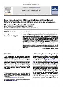
333 partial differential equations being solved for. The stress in the deposited films is obtained via a flex wafer curvature measurement system. In addition to this stress, the simulations also account for a thermal mismatch stress between various layers. The mismatch temperature gradient is obtained from the difference in the average deposition temperature (400°C) of various films and room temperature (25°C). Positive stress is tensile while negative stress is compressive in this work's definition of stress. The lateral (S xx ), vertical (S yy ), and shear (Sxy) stress components for a typical tungsten plug structure are shown in Figure 1. The bulk of the aluminum and tungsten are under tensile stress, while the oxide immediately adjacent to these films is in compression. This is true for both S xx and S yy . The shear component (Sxy) represents a twisting motion in a plane perpendicular to the plotted structure and peaks at the four corners of the tungsten plug.
3. Effect of Electromigration Induced Depletion The effect of depleting the aluminum in the lower aluminum (metal 1) layer on the stress distribution in the structure was also investigated. The depleted region was represented as a "soft" material with no thermal mismatch with the adjoining materials. This was done to avoid singularity problems in the finite element solution of the system. Figure 2 shows S xx , S yy , and S xy for a depleted tungsten plug structure. The depletion is assumed to extend to the immediate right of the tungsten plug. The depleted aluminum edge leads to the formation of a highly tensed region immediately above the depleted edge into the TiN (ARC) film and extending into the oxide. This is evident in the plot for S xx and S yy . Similar stress analysis (Figure 3) for a highly depleted structure (where the depletion extends through most of metal 1) indicates that the highly tensed region falls of rapidly in the S xx plot: the tensed (red/dark) region above the depletion edge almost vanishes. A relatively gradual fall in S yy and S xy components is observed as well (Figure 3). The simulations suggest that the proximity of the tungsten plug to the metal 1 depletion edge plays an important role in determining this region of high tensile stress in the TiN film which forms the ARC. Interestingly, the location of this highly tensed region corresponds to the appearance of cracks or open circuits in the ARC layer as observed in cross-sectional micrographs of the stack (Figure 4). Electrical measurements exhibit a very large increase in via resistance of the plug during stress testing of the tungsten plugs. Electrical simulations suggest that this large increase in via resistance cannot solely be explained via the depleted aluminum. However, the large increase in the measured via resistance can be explained if a discontinuous (or cracked) TiN film exists during electromigration. The stress simulations thus provide a possible explanation of these mechanical and electrical phenomenon.
4. CONCLUSION The origin of cracks or open circuits observed in cross-sectional micrographs in tungsten plug stacks is explained via the appearance of a highly tensed region in the finite clement stress simulations. The presence of the electromigration induced metal 1 depletion edge in proximity to the tungsten plug is responsible for this high stress in the tungsten plug stack. The hitherto unobserved phenomenon adds another dimension to the long term reliability characterization of tungsten plug structures.
334 REFERENCES: [1] T. Kwok, C. Tan, D. Moy J.J. Estabil, H.S. Rathore, and S. Basavaiah, Proceedings of VLSI Multi-level Interconnect Conference, (1990), p. 106. [2] S. Domae, H. Masuda, K. Tateiwa, Y. Kato, and M. Fujimoto, The 36th Annual Proceeding of the IEEE Reliability Physics Symposium (Reno, NA, IEEE, 1998), p. 318. [3] L.J. Elliott, T. Spooner, J.H. Rose, and R. Shuman, Mater. Res. Symp. Proc. 391, (San Fransisco, CA, Material Research Society, 1995), p. 459. [4] J.A. Walls, IEEE Trans. Electron Dev. Lett., 16,430 (1995). [5] J.S. Huang et al., Lucent Technologies, Orlando, FL, unpublished. [6] Mark E. Law, FLOOPS manual. [7] Medici user's manual, Vol. 3, TMA, Feb. 1997.
•Ill -Lll •Ul
Km
B.W
tat
•i iiB IBM w SI B 1111 M^k;.,*
IHN tScii-'""'
LU
•ug- »»s function of the lateral position of the depletion edge. crack corresponds to the stressed region shown in rig ure 2.


![free [download] finite element simulations with ansys ... - Google Sites](https://m.moam.info/img/260x300/free-download-finite-element-simulations-with-ansy_6478ad6a097c474d228d6b1c.jpg)
![[PDF] Download Finite Element Simulations with ... - Google Sites](https://m.moam.info/img/260x300/pdf-download-finite-element-simulations-with-googl_6478ad6a097c4786708d16fb.jpg)