Countermeasures Against Fault Attacks on Software Implemented AES: Effectiveness and Cost Alessandro Barenghi
Luca Breveglieri
Israel Koren
DEI – Dipartimento di Elettronica e Informazione Politecnico di Milano Via Ponzio 34/5, 20133 Milano, Italy
DEI – Dipartimento di Elettronica e Informazione Politecnico di Milano Via Ponzio 34/5, 20133 Milano, Italy
Department of Electrical & Computer Engineering University of Massachusetts Amherst MA 01003, USA
[email protected]
[email protected]
[email protected]
Gerardo Pelosi
Francesco Regazzoni
DEI – Dipartimento di Elettronica e Informazione Politecnico di Milano Via Ponzio 34/5, 20133 Milano, Italy
UCL Crypto Group, Université Catholique de Louvain ALaRI – University of Lugano Via G. Buffi 13, CH-6904 Lugano, Switzerland
[email protected]
[email protected]
ABSTRACT
Categories and Subject Descriptors
In this paper we present software countermeasures specifically designed to counteract fault injection attacks during the execution of a software implementation of a cryptographic algorithm and analyze the efficiency of these countermeasures. We propose two approaches based on the insertion of redundant computations and checks, which in their general form are suitable for any cryptographic algorithm. In particular, we focus on selective instruction duplication to detect single errors, instruction triplication to support error correction, and parity checking to detect corruption of a stored value. We developed a framework to automatically add the desired countermeasure, and we support the possibility to apply the selected redundancy to either all the instructions of the cryptographic routine or restrict it to the most sensitive ones, such as table lookups and key fetching. Considering an ARM processor as a target platform and AES as a target algorithm, we evaluate the overhead of the proposed countermeasures while keeping the robustness of the implementation high enough to thwart most or all of the known fault attacks. Experimental results show that in the considered architecture, the solution with the smallest overhead is per-instruction selective doubling and checking, and that the instruction triplication scheme is a viable alternative if very high levels of injected fault resistance are required.
C.3 [Special-Purpose and Application Based Systems]: Microprocessor/microcomputer applications; C.5.3 [Computer System Implementation]: Microcomputers—portable devices; E.3 [Data Encryption]: Standards (AES)
General Terms Security
Keywords Side-Channel Attacks, Fault Attacks, Countermeasures
1. INTRODUCTION Embedded systems now constitute the largest segment of the electronic consumer market. Such a position was gained thanks to their diffusion in our everyday life, in diverse applications such as fuel injection in cars, access control systems and smart-cards. Many of these applications require the use of cryptographic algorithms to secure the data that they process. The widespread use of security-sensitive embedded systems brings up new design challenges. Although the traditional design objectives such as power consumption, memory usage, real time performances and reconfigurability continue to be important, the use of embedded systems for critical functions makes security one of the most significant requirements of the system design. Among the possible attacks proposed in the past, the ones which target the physical implementation of the cryptographic algorithm are the most dangerous, since they are often easy enough to be successfully carried out. Fault injection attacks, in particular, have proven to be a very effective and relatively inexpensive way to retrieve the secret information processed by electronic devices. In a typical fault attack scenario, the adversary injects a number of faults during the computation of a cryptographic routine and then analyzes the faulty outputs to derive the secret key of the cipher. Recent works have improved this technique through
significantly reducing the effort required to mount a fault injection attack, thus raising the threat level posed by them. The results presented in [4, 15] have provided key insights into how to induce faults through the use of reasonably cheap equipment and simple workbenches by varying the feeding voltage of an ARM-based device, resulting in predictable corruptions of the values loaded from the memory. This kind of faults can be injected with almost no knowledge about the implementation details of the cipher and should therefore, be regarded as particularly dangerous. Through the use of more sophisticated workbenches (e.g., laser injection stations [17] or timed EM-pulses [1]) it is also possible to inject errors into a device in a time accurate way. This kind of attack, albeit as viable as the previous one, requires a higher level of technical knowledge and more expensive equipment and is therefore, regarded as realistically applicable only in cases where highly valuable goods are at stake. In [3] it was shown that widely deployed embedded processors can be attacked through judiciously lowering the processor’s supply voltage. The induced faults can be injected with very high precision into instructions which fetch data from memory and then, through exploiting the resulting faulty ciphertexts, the secret key of a cipher can be easily inferred. A wide range of fault injection techniques have been discussed in [2], which provides a comprehensive summary of the technological possibilities available to a want-to-be attacker. Manufacturers of embedded devices developed a large variety of hardware countermeasures that are incorporated into the design to counteract specific types of physical attacks [18]. One important group of such countermeasures relies on the use of sensors and filters such as anomalous frequency detectors, anomalous voltage detectors, or light detectors. Commonly used countermeasures include randomized clock to achieve an unstable internal frequency, insertion of dummy random cycles, and the use of active and passive shields to protect the internal circuits. Another kind of countermeasures doubles the hardware resources to perform the same computation in parallel or use the same components to recompute the results twice. This approach however, has not been widely adopted since it proved to be expensive and not fully satisfactory with respect to advances in the techniques used to carry out the attacks. The adoption of pure hardware-based countermeasures has several drawbacks. Highly reliable countermeasures turn out to be expensive and usually not easily applicable to a wide range of platforms, while moderately priced countermeasures only detect specific attacks. Since the development of new fault attacks is a continuous threat, detection of currently known forms of physical tampering is not sufficient against future developments. Thus, most hardwarebased countermeasures cannot guarantee an effective errorprevention behavior with satisfactory cost vs. performance tradeoffs. Software countermeasures, in contrast, can benefit from both easier deployment and potentially better cost to performance ratio, and thus constitute an essential component in attempts to counteract as many different kinds of attack as possible. In this paper we present a methodology to introduce a tailored per-instruction redundancy in the Advanced Encryption Standard (AES) algorithm: the most widely deployed symmetric block cipher. Our countermeasures target soft-
ware implementations of AES running on any ARM platform from ARM7 (ARMv3 architecture) onwards, thus encompassing the most commonly used processor in embedded devices in the last 16 years. The proposed countermeasures take into account the main memory architecture of the chip, and can be applied even when the cipher source code is not available, thus reducing the deployment cost. The paper is organized as follows. Section 2 provides a brief summary of the AES block cipher chosen as a case study and describes the target architecture. Section 3 presents the proposed countermeasures, and Section 4 reports the results of the experimental campaign conducted in order to ascertain the effectiveness of the proposed methods. Section 5 surveys the related work and Section 6 presents our conclusions.
2. APPLICATION SCENARIO In this section we briefly describe both the cipher of choice and the target architecture used to validate the proposed countermeasures.
2.1
AES Overview
Our proposed countermeasures against fault attacks support a tunable level of protection, thus providing a full spectrum of trade-offs between the level of protection and the implementation overhead. We focus here on the AES cipher [7], which is employed in a wide range of devices. The AES cipher executes a number of round transformations on the input plaintext, where the output of each round is the input to the next one. The number of rounds r is determined by the
1 2 3 4 5 6 7 8 9 10 11 12 13
Algorithm 2.1: AES Encryption Input: p, plaintext block; k, cipher key Output: c, ciphertext block begin hk(0) , k(1) , . . . , k(r) i KeySchedule(k) c AddRoundKey(p, k(0) ) foreach i ∈ {1, . . . , r} do c SubBytes(c) c ShiftRows(c) c MixColumns(c) c AddRoundKey(c, k(i) ) c SubBytes(c) c ShiftRows(c) c AddRoundKey(c, k(r) ) return c end key length: a 128-bit key uses 10 rounds, a 192-bit key uses 12 and a 256-bit key uses 14. In software, AES can be implemented using only bitwise xor operations, table-lookups and 1-byte shifts [7]. Each round is composed of the same steps, except for the first where an extra addition of a round key is inserted, and the last where the (MixColumns) operation is skipped. Each step operates on 16 bytes of data (referred to as the internal state of the cipher) generally viewed as a 4×4 matrix of bytes or an array of four 32-bit words, where each word corresponds to a column of the state table. The four round stages are: AddRoundKey (xor addition of a scheduled round key), SubBytes (byte substitution by a lookup table (S-box)), ShiftRows (cyclical shifting of bytes), and MixColumns (linear transformation which mixes column
state data). Given the cipher key k, the KeySchedule procedure outputs r+1 round subkeys, with each subkey being 16 byte wide. Algorithm 2.1 shows the complete encryption process. The encryption procedure is amenable to several software implementations which trade-off memory and computational resources in order to obtain the best performance for the given architecture. Specifically, the different steps of the round transformation can be combined into a single set of table lookups, allowing for very fast implementations on processors having word length of 32 bits or more [7]. Denote by ai, j , i, j ∈ {0, 1, 2, 3}, the generic element of the state table, by a the value of a byte variable, by S[0, . . . , 255] the 256 bytes of the S-box table and by ◦ a GF(28 ) finite field multiplication [7]. Let T0 , T1 , T2 and T3 be four lookup tables, each viewed as a sequence of 256 32-bit words, containing results from the round operations as follows: T0 [a] = [ S[a] ◦ 02; S[a]; S[a]; S[a] ◦ 03 ]
memory access latency is lower than the computation time that would be required in place of each T -table lookup. On the other hand, in cache constrained environments a valid alternative to the use of T -tables is the computation of the entire AES rounds on the processor, memorizing only the S-box and the inverse S-box tables needed to perform the substitution operations. Another downside of employing D-caches, regardless of the constrains on the size of the chip, is represented by cache timing attacks to cryptographic algorithms. This kind of attack makes it possible to infer from the loading times of a value, its position in the main memory, and thus obtain information on the memory access patterns of a cipher. This in turn has been demonstrated to be sufficient for breaking AES in [20], and thus the employment of cache should be either avoided or carefully regulated during the execution of this algorithm.
T1 [a] = [ S[a] ◦ 03; S[a] ◦ 02; S[a]; S[a] ]
2.2
T2 [a] = [ S[a]; S[a] ◦ 03; S[a] ◦ 02; S[a] ]
The target architecture to validate our countermeasures is the ARM family of processors. Our proposed countermeasures are employable on every ARM processor starting from ARM7 (ARMv3 architecture). ARMv3 is a load-store RISC machine, where every instruction is executed in one clock cycle, and may be conditioned by a flag in the program status word. This feature was introduced in order to compensate for the missing branch predictor which was introduced only later into ARM8 processors. The load instructions are not bound to be executed in a single cycle; instead, they may stall the pipeline until the information is retrieved from the main memory. The memory latencies have a broad range due to the wide field of applications in which the ARM processor is deployed. The RISC architecture and the fully predicated instructions (which are used in place of small decisional constructs) make the ARM architecture suitable for use in low power or memory constrained environments. This has made them dominant in the mobile and embedded electronics market. Thanks to its high power efficiency, the ARM architecture has been lately employed also in mobile multimedia enabled platforms. This, in turn, has lead to an increase in the computing power and memory demand from the platform, leading to the formation of the same CPU-Memory speed gap experienced in high-end microprocessors. In order to cope with the increasing demands for higher performance, the latest ARM-based platforms are split, according to the target use, into two families, Cortex-A and Cortex-M, while retaining full binary compatibility. CortexA based platforms target high-end mobile multimedia devices, and are often endowed with two levels of caches to cope with the load latency of high capacity but slow off-chip memory. The L1 cache is split into two halves, which are used as dedicated instruction (I-cache) and data cache (D-cache), while the L2 cache is unified for both data and instructions. The Cortex-M family targets the microcontroller and highly energy constrained environments. For this CPU family, the Cortex-M3 reference manual from ARM1 suggests the use
T3 [a] = [ S[a]; S[a]; S[a] ◦ 03; S[a] ◦ 02 ] These tables are used to compute the round operations as a whole, as described by the following equation, where kj is the j-th word of the expanded key and Aj =ha0,j , a1,j , a2,j , a3,j i is the j-th column of the state table considered as a single 32-bit word (with the simplified notation: Aj = Aj mod 4 , ai,j = ai, j mod 4 ): Aj = T0 [a0,j ] ⊕ T1 [a1,j−1 ] ⊕ T2 [a2,j−2 ] ⊕ T3 [a3,j−3 ] ⊕ kj The four tables T0 , T1 , T2 and T3 (called T-tables from now on) use 4 KB of storage space and their main goal is to avoid performing the MixColumns and InvMixColumns transformations as these operations, in the original definition of Rijdael algorithm, perform Galois Field multiplications by fixed constants which map poorly to general-purpose processors in terms of performance. Notably, in the final round of the encryption there is no MixColumns operation, and the KeySchedule algorithm requires pure substitution operations. While these facts could represent an impairment to the use of T tables, it is possible to extract efficiently the S table through proper masking of the T tables. Since the T -tables may be derived also through rotating each word of T0 by i bytes, Ti [a] = RotByte(T0 [a], i), i ∈ {0, . . . , 3}, in order to reduce the active memory footprint used within each round, every column of the state table may also be computed as: Aj = T0 [a0,j ] ⊕ RotByte(T0 [a1,j−1 ], 1)⊕ ⊕RotByte(T0 [a2,j−2 ], 2) ⊕ RotByte(T0 [a3,j−3 ], 3) ⊕ kj This variation reduces the lookup tables to a single 1 KB one, thus lowering the burden on the caches, while incurring a penalty of only three extra rotations per column per round with respect to the four T -tables implementation. Decryption requires different tables from those used by the encryption. Therefore, an AES implementation able to perform both encryption and decryption may require up to 8 KB of memory, which may extend to 16 KB if the last round operations are implemented using ad-hoc tables. When employing general-purpose processors, endowed with large Dcaches, the T -table implementation is more efficient since the
1
Target Architecture
Cortex-M3 Technical Reference Manual (July 2010): http://infocenter.arm.com/help/topic/com.arm.doc. ddi0337e/DDI0337E_cortex_m3_r1p1_trm.pdf
of tightly coupled memories: i.e., small amounts of SRAM integrated on the same die with the microprocessor, and characterized by very low access latencies (one or two clock cycles). Embedding the memory in the same chip eliminates the need for caches since the main memory is implemented with cache-like timing features. Furthermore, the power consuming circuits driving the caches are not needed. While typical memory access latencies for chips having ondie integrated memory range from one to two clock cycles, off-chip DRAM memories tend to require up to 64 CPU clock cycles to fetch the data. The ARM architecture has 16 general-purpose 32-bit registers. Although the architectural specification does not impose any restriction on their usage, the standard ARM ABI interface mandates the use of the last three registers (r13r15) for keeping the context of the running program (stack pointer, link register and program counter). Moreover, the content of r12 is not guaranteed to be preserved between function calls, thus acting as a scratch register. In order to provide fast shifting and rotation of loaded values, one of the two loading lines for the ALU has a 32-bit barrel shifter able to act without delaying the loading of the value from a register into the ALU. This implies that it is possible to perform computations directly with a shifted or rotated operand without losing an extra clock cycle.
3. COUNTERMEASURES In this section we explore the incorporation of error detecting and correction techniques into the AES algorithm implemented in software and executed on the ARM platform without modifications to either the Application Binary Interface (ABI) or the underlying architecture. The most straightforward countermeasure against fault attacks is to run the same cryptographic algorithm twice for each input, and subsequently check if the results match. This technique may be extended to triplicating the execution of the algorithm in order to achieve single-error correction capabilities by applying majority voting to the results. The duplication method works well against naturally occurring faults, but may be less effective against maliciously injected ones. In fact, a motivated attacker may be able to bypass these countermeasures through injecting two faults, one for each execution of the algorithm. With the currently available fault injection technologies it is possible to induce faults with very accurate timing during the execution of a software routine [14]. Indeed, it is possible to inject faults with a single clock cycle accuracy in different runs of the same algorithm, while it is practically infeasible to inject faults in subsequent instructions with most of the currently available fault injection techniques. We note that two fault injections in two subsequent instructions could be still achieved by using two synchronized laser injection apparatuses and a semi-transparent mirror. This would require a highly competent attacker with considerable means, and thus would be viable only against very valuable targets. On the other hand, EM pulses, supply voltage alterations, clock glitching techniques [2, 16] and other low cost fault injection techniques do not possess the precision required to inject such faults. In order to thwart attacks that target the same instruction during two consecutive executions of the same code, we propose to apply redundancy at a finer grain, i.e., at the single instruction level. We consider three ways of inserting redun-
dant computations and the subsequent checking: instruction doubling to detect errors, instruction triplication to add error correction capabilities, and computation of parity bits to be checked against stored values. The latter countermeasure though, may only be applied to load operations in our scenario since it requires the expected parity bits to be computed in advance for the result of the protected operations. In order to provide a fair comparison, we evaluate both a full instruction duplication/triplication strategy, and the protection of the load instructions only. These countermeasures can be either applied to the whole cryptographic algorithm or only to the parts that are known to be vulnerable to attacks (Selective Insertion) in order to reduce the computational overhead. The advantage of applying the selected scheme to the entire algorithm is the greater ease of application, since the insertion of the countermeasure can be done directly into the code obtained by disassembling the executable object code, without knowing any details about the algorithm implementation, and with no need to take into account the optimization strategies of the compiler to prevent the removal of redundant operations. The only issue in applying per instruction redundancy is represented by the “Branch and Link” ARM instruction, since it could create duplicated stack frames. This problem can be solved through the use of inline functions to implement the algorithm, thus avoiding the generation of the aforementioned instruction by the compiler. The selective insertion technique requires some knowledge of the encryption program structure in order to locate the sensitive parts which need the application of the countermeasure. For example, in the considered AES case study, all the known attacks focus either on the last three round operations or the first subkey addition [3, 8, 9, 12, 13, 15, 19]. Therefore, when either the algorithm structure or the source code is known, it is possible to protect the implementation of the algorithm with a reduced overhead.
3.1
Instruction Duplication (ID)
The first method examined is duplicating the execution of certain (or a specific class of) instructions and storing the second result into a different register of the CPU. This is possible in our implementation since the AES algorithm uses only 9 registers (in our binary r1–r9) of the ARM architecture, thus leaving 4 registers available for our purposes (r0, r10–r12). After repeating the instruction, the results are compared, and if a mismatch is detected, the inserted code jumps to an error management routine which may either signal the error or fill the state of the computation with random numbers to avoid information leakage. The following code sample illustrates the insertion of the ID countermeasure to protect the load of a value in r4 from a memory location whose address is contained in r7: 1. 2. 3. 4.
ldr ldr cmp bne
r4,[r7]; r12,[r7]; r12,r4; ;
This kind of countermeasure fails to detect two types of faults: two identical faults injected in each of the payloads
of the load operations, and a single fault injected in a load and an instruction skipping fault which allows to bypass the branch instruction (bne) after the comparison.
3.2 Instruction Triplication (IT) The second method (IT) repeats an instruction three times and stores the two extra results into two unused registers. In the following code snippet the protected instruction is an exclusive-or (eor) between r1, r2 with result stored in r4: 1. 2. 3. 4. 5. 6. 7.
eor r12,r12,r12; eor r10,r1,r2; eor r0,r1,r2; eor r4,r1,r2; cmp r4,r10; eoreq r12,r12,#1; cmp r4,r0;
8. 9. 10. 11. 12. 13. 14.
eoreq r12,r12,#2; cmp r10,r0; eoreq r12,r12,#4; cmp r12,#0 beq ; cmp r12,#4; moveq r4,r0;
This technique employs a fourth register, r12 to record the effects of the correctness checks (lines 5–10) and determine whether to correct a single error (lines 13–14), detect two errors (lines 11–12) or leave the result unchanged. The eor operation between r1, r2 is performed thrice and the three results are stored in the target register (r4) and in two scratch pad registers (r10, r0). The algorithm then proceeds to check the equality of the values pairwise and stores the result of the comparison as a single bit flag in register r12 which was zeroed at the beginning. To save comparison instructions, the previous code snippet checks only if either the first value (which has already been loaded into the target register) is faulty or not, and eventually corrects it without taking care to correct the values in the two scratch pad registers. An attacker may attempt to thwart the instruction tripling countermeasure by injecting two identical faults into two of the three sensitive operations. This implies that the attacker must be able to interfere with the execution of two instructions, which are only a single clock cycle apart, in exactly the same way. Another alternative is to inject a fault during the operation that will set the correct output register (i.e., not one of the redundant ones; r4 in the example) and subsequently skip both the branch to error instruction and the last moveq instruction, which would restore the correct result. This would mean being able to inject one data altering fault and two instruction skip faults within an 11 clock cycles timeframe, with the middle fault being 2 clock cycles apart from the last.
3.3 Parity Checking (PC) The third technique considered (PC), is a tabulated parity bit to check the consistency of values fetched by a load instruction. This technique is not readily applicable to generic arithmetic/logic operations since it requires the prediction of the resulting parity bit prior to the instruction execution. Another disadvantage of employing parity in software is the fact that the parity bit related to each protected value must be computed from the corresponding word, at the expense of additional computation steps. Moreover, the storage of parity bits is troublesome in software since the parity bits might
be stored either in a bit-packed form (which requires extra operations to decode) or in a sparse representation (i.e., 1 bit per byte/word), which wastes a considerable amount of memory (e.g., an entire byte is reserved for storing a single parity bit). The following code snippet represents a straightforward way to compute the parity bit of a value contained in r4, and referenced by r1 in order to check it against a precomputed value stored in memory at the address contained in r7. 1. 2. 3. 4. 5. 6.
ldr mov lsr eor lsr eor
r4,[r1]; r12,r4; r0,r4,#4; r12,r12,r0; r0,r12,#2; r12,r12,r0;
7. 8. 9. 10. 11. 12.
lsr eor and ldr cmp bne
r0,r12,#1; r12,r12,r0; r12,r12,#1; r6,[r7]; r12,r6; ;
The protected value in r4 may either correspond to a byte of the lookup table used in the AES implementation (S-box or T -table) or to a byte of the unrolled key. The code computes the parity bit through xoring a value obtained from a shifted copy of the one whose parity is checked. The parity value is accumulated in a scratch pad register (r12) and employs a temporary register (r0) to store the correctly shifted copy of the value whose parity is computed. After all the bits of the byte are added, the final value is masked with a single bit mask and compared to the correct parity which is loaded from the memory at line 10. Since the ARM architecture has a barrel shifter capable of shifting/rotating one of the two operands of an arithmetic/logic instruction, it is possible to skip altogether the use of the temporary register and considerably reduce the number of instructions needed to compute the parity as shown in the following code: 1. 2. 3. 4. 5. 6. 7. 8.
ldr eor eor eor and ldr cmp bne
r4,[r1]; r12,r4,r4, LSR #4; r12,r12,r12,LSR #2; r12,r12,r12,LSR #1; r12,r12,#1; r6,[r7]; r12,r6; ;
As for the achieved fault coverage, parity codes are capable of detecting half of all possible faulty results of the operation they are protecting since any multi-bit injected fault with an even number of bit flips will not be detected. An attacker can bypass the protection scheme by injecting faults both during the load operation and during either the branch instruction after the comparison or the loading of the correct parity value.
3.4 Fault Coverage Summary Table 1 summarizes the fault detection capabilities and fault coverage of the previously described approaches. An important observation emerging from the table is that countermeasures that provide full coverage of faults, also require a higher temporal precision from a potential attacker in order to be thwarted. In particular, the second fault should be injected during a specific clock cycle that is only 3 to 10 cycles apart from the first fault. Such a tight timing is a very difficult to achieve with the current fault injection techniques, which require a non negligible amount of time to reset the fault inducing means (laser, EM and clock glitcher apparatuses are characterized by large capacitors which require a long time to be recharged) [16]. Table 1: Fault coverage and minimum required faults to subvert a countermeasure Counter -measure
Fault Detection [%]
Instr. Skips Required
Instr. Distance
ID IT PC
100 100 50
2 2 1
4 11 6
Since this resetting time greatly exceeds the required 10 clock cycles, even for implementations running at very limited clock rates, the proposed countermeasures may be regarded as safely preventing the successful injection of faults for all the present implementations. A key point of employing a parity bit as protection mechanism is that it cannot detect errors that were inserted during computations, thus leaving a possible target for attackers. However, the low cost and easy to set technique described in [4] is only able to inject faults in the load operations executed on an ARM architecture and thus would be detected by a parity bit check. The difficulty of injecting two or more faults within a period of 11 or fewer clock cycles does not exist when the entire code is duplicated (or triplicated) and only the final results are compared. Such replication provides a large time gap between the two fault injection points, allowing the attacker to properly reset the fault injection equipment.
3.5 Effects of the Caches Many high-end ARM-based embedded systems (see Section 2.2) integrate one or two levels of cache units in their design. This architectural feature has a direct impact on the fault injection countermeasures since it implies that the erroneous result of an operation may be reused by the CPU if the wrong computed or loaded value is held in a cache. This is of particular concern when load instructions are replicated since inducing a fault in a single load instruction implies that all the subsequent ones will be using the same faulty value held in the data cache. Such a side effect would nullify the load replication countermeasures since all the comparisons would act on the same faulty value and fail to detect the error. This side effect (due to the presence of a cache) may also affect the technique that duplicates the full execution of the AES algorithm, since the round key and S-box values are preserved in the data cache during the duplicated executions.
The most straightforward solution to this problem is to disable the cache altogether. This can be done at runtime for the entire duration of the encryption algorithm, but will result in a substantial performance penalty. An alternative solution is the use of per-line cache invalidation, which is available in the ARM architecture through the mcr instruction. Through selective invalidation of the cache lines containing the values which have just been loaded, it is possible to avoid storing faulty data in the cache. Since only the duplicated instructions would require cache invalidation, the other parts of the algorithm that do not need protection can still benefit from the presence of the cache. Another advantage of flushing the cache lines containing the sensitive values is the intrinsic protection against the timing attacks mentioned in [20], since it is no longer possible to make any inference regarding the position of the values loaded with respect to the loading times within the algorithm. The invalidation of cache lines would require additional instructions that must be placed right before every sensitive instruction in the code, in order to warrant a fresh load from main memory. Thus, all the aforementioned listings will be extended by a number of mcr instructions that is equal to the number of ldr instructions performed, since the whole inner state of the AES cipher is kept in the registers, which in turn implies that there are no memory writeback operations which need to be taken care of. It is important to notice that the traditional duplication/triplication methods applied at the algorithm level will also need to flush the cache between the repeated executions of the algorithm, otherwise they would suffer from the same problem. In order to minimize the impact of the cache line flushes, it is possible, if the source code of the algorithm is available, to align all the sensitive variables to the same cache lines by using compiler directives such as the DCACHEALIGN of GCC. These directives, provided the cache line size is known, allocate the variables so that their beginning in memory is aligned to a cache line, thus resulting in minimal trashing of unrelated values when a cache line is flushed. Employing this technique would reduce the performance penalty. The following section presents the cost of the studied countermeasures in both cache-endowed and cache-free environments, thus covering the entire range of embedded systems based on ARM CPUs.
4. COUNTERMEASURES EVALUATION In this section we discuss the efficiency of the proposed countermeasures when applied either to the full cipher or to a selected subset of only the sensitive instructions based on known attack points. The findings in [3, 8, 9, 12, 13, 15, 19] suggest that injecting a fault within the last three rounds of the AES cipher leads to successful attacks allowing a complete key recovery with as few as 6 faults for AES-256. It is thus mandatory to protect the last three rounds in full, in order to prevent these attacks from succeeding. The attack in [6] addresses another fault injection technique capable of discovering the full key through injecting singlebit errors during the first key addition. This implies that also the first key-load and addition must be protected against faults. The safe-error attack in [6] consists of injecting a fault during the algorithm execution and checking whether it
120000
80000
TMR PAR DMR PAR-barrel None
35000 Execution time [cycle]
100000 Execution time [cycle]
40000
TMR PAR DMR PAR-barrel None
60000 40000 20000
30000 25000 20000 15000 10000 5000
0
0 1
2
4
8
16
32
64
1
2
4 8 16 Load cost [cycle]
Load cost [cycle]
(a)
32
64
(b)
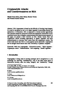
Figure 2: Execution times of AES with protection of all the load instructions of the algorithm (a), and with protection of only the instructions in the last three rounds (b) impacts the expected result. Therefore, this attack requires the countermeasure designer to provide an error correction mechanism to produce a correct result regardless whether a fault has been injected or not. Even if the AES implementation outputs a randomized value (instead of the actual faulty ciphertext) or simply signals an error without outputting anything, the attack proposed in [6] will still be able to extract information since it only relies on detecting an anomaly in the correct functioning of the circuit. However, the fault injection capabilities required to mount this attack are very high and thus, it is reasonable to consider incorporating an error correction mechanism only if the cipher is protecting significantly valuable goods. The implementation of AES-128 used to validate our proposed countermeasures is a T -table based implementation, realized in C and compiled for the ARM9 architecture, employing release grade optimizations (-O2) with GCC 4.0.2. Since the ARM architecture provides free rotations through the barrel shift unit, the most efficient implementation is the one employing only a single T -table and rotating on the fly the obtained value to get the correct 32-bit word to
Execution time [cycle]
250
PAR PAR-barrel TMR DMR None
200 150 100 50 0 1
2
4 8 16 Load cost [cycle]
32
64
Figure 1: Execution time required to protect a single load instruction as a function of the clock cycles needed to fetch the value from memory (no cache units available)
Table 2: Countermeasures overhead per single instruction to be protected Counter -measure None ID IT PC PC-barrel
Instruction Count
load Count
No. of extra Registers
1 4 14 12 8
1 2 3 2 2
0 1 3 3 2
update the state of the cipher, as described in Section 2.1. The compiled object was subsequently disassembled and the countermeasures were introduced directly into the assembly listing. Table 2 presents the overhead, expressed in number of clock cycles, needed for each countermeasure to protect a single instruction. The overhead has been split into individual components, namely, the extra computational instructions inserted, the additional loads and the number of scratch registers required. The results show that employing the IT scheme has the highest computational cost. On the other hand, it is the only scheme that provides error correction, while the others can only detect a fault during the execution. The ARM code for parity checking is more computationally intensive than the simple instruction doubling, and has the additional drawback of not being applicable to computational instructions. Figure 1 shows the execution time needed to protect a single load instruction as a function of the number of clock cycles required to fetch a value from memory when no caching mechanism is available. When a cache is available, the overhead introduced by the insertion of cache flushing instructions amounts to a few cycles with respect to the results reported in Figure 1, and will therefore have, a limited impact on the comparison among the countermeasures. The costs range from an ideal of a single cycle (which may happen in case the value is held in tightly coupled memories, typical of small embedded systems) to 64 cycles for slow off-chip memory. From the figure one can notice that the ID scheme
is uniformly less expensive than the parity schemes regardless of the latency of the memory, while providing the same error detection capability. The IT scheme has the highest overhead among all the countermeasures, and the overhead with respect to the parity checking remains below 40% only for memory latencies lower than 8 cycles. This in turn implies that IT is a viable choice in the case the main memory is tightly coupled with the core. Figures 2(a) and 2(b) depict the execution times for the AES-128 algorithm when applying protection to every load instruction in all the rounds, and when selectively protecting only the sensitive portions of the algorithm (i.e., the ldr instructions in the last three rounds plus the initial key addition). The results in these two figures confirm the intuition deduced from the single load overhead investigation, suggesting ID as the cheapest fault detection scheme and IT as a reasonably lightweight alternative if error correction is desired and a fast memory is available. The comparison between applying the countermeasure to all the load instructions (Figure 2(a)) and the selective application to the sensitive load instructions only (Figure 2(b)) shows an advantage by a factor of three in terms of clock cycles overhead. The slowdown of the instruction tripling method with respect to the ID and PC methods is constant over the whole memory latency range.
140000
Full-IT Full-ID 3 Round-IT 3 Round-ID None
Execution time [cycle]
120000 100000 80000 60000 40000 20000 0 1
2
4
8
16
32
64
Load cost [cycle]
Figure 3: Execution times of AES with protection applied to every instruction
Figure 3 shows the execution time of the AES-128 algorithm, and compares the impact of the instruction doubling and the instruction tripling countermeasures when applied to every instruction of the algorithm or only to the instructions belonging to the last three rounds. The figure clearly demonstrates that focusing on the sensitive portions of the algorithm allows to achieve up to a 70% improvement compared to the solution that blindly protects every instruction. Moreover, as shown in Table 3, the execution time of a protected implementation does not significantly exceed the slowdown experienced when executing the algorithm twice or thrice, respectively. Table 3 summarizes the countermeasures proposed in this paper together with the performance costs ensued from their application. The memory latencies of 2 and 64 cycles were chosen among the ones considered in the exploration since they represent two typical application scenarios. The 2-cycle access latency is characteristic
of tightly coupled on-chip SRAMs which are able to provide fast memory access albeit only for small quantities of it. The 64-cycle access time is a reasonable representative of off-chip DRAM banks, employed when large memories are required and the system design includes a full memory management unit, together with load- and write-buffers. A key point in chips with tightly coupled memories is the fact that they are never endowed with caches, due to the very fast access to the main memory. This in turn implies that it is never necessary, in that scenario, to add the cache flushing instruction in order to avoid the faults lingering in cache. A side effect of increasing the memory latency is the fact that computationally intensive countermeasures will behave proportionally better with slow memories, since the overhead introduced by the extra operations will be dwarfed by the large amount of clock cycles required to access the memory. The second pair of rows in Table 3 reports the performance cost of protecting all the instructions using ID and IT, respectively. Albeit at a higher cost, these schemes provide complete protection against any possible injected fault, both in the computational instructions or during memory accesses. Of particular interest are the results obtained when protecting the last three rounds using ID: the execution time costs are lower than those for duplication of the whole computation, while retaining the benefits of perinstruction consistency checking. Another noteworthy result is for the case when IT is applied to the whole algorithm on devices with slow memories. In this case, the overhead is only 12% higher than triplication of the entire algorithm. It is thus possible to apply instruction level triplication, which has correction capabilities and provides a complete protection against all known fault attacks using all the currently known fault injection techniques. Comparing the methods which protect only load instructions (3rd and 4th pair of rows in Table 3) suggests that proper selective duplication is cheaper than all the other methods, including duplicating the entire cipher. Moreover, this scheme also provides a stronger protection than the full algorithm duplication, as reported in Section 3, due to the stricter bounds imposed on the attacker capabilities. The IT scheme, when applied only to the sensitive portions of the code, results in a reasonably lightweight scheme, keeping the overhead near that of the triplication of the entire algorithm. This suggests that IT is a viable alternative when error correction is desired, e.g., when the attacker has powerful means and is able to exploit the safe error attack proposed by Bl¨ omer [6]. The slowdown introduced by the addition of the cache flushing instructions is negligible by itself, even if a line invalidation instruction per-load must be issued. Employing per-line invalidation has also the advantage over more coarse methods (whole cache invalidation) by not trashing the full contents of the cache thus preserving the contents related to other tasks which may be running on the same system.
5. RELATED WORK Previous work has mostly focused on hardware implementations [2] and on solutions based on error detection codes [5, 10, 11]. Several Concurrent Error Detection (CED) techniques has been adapted to the specific needs of cryptographic algorithms. Every time an error is detected, the normal execution of the algorithm is stopped to prevent the generation of wrong outputs. As a result, the attacker is unable to view and analyze the faulty outputs.
Table 3: Performance cost for all the proposed countermeasures schemes. * indicates the slowdowns taking into account the cache line flushing operations Countermeasure
Last Three Round Protection load cycles: 2 load cycles: 64
Algorithm Duplication Algorithm Triplication
Whole Algorithm load cycles: 2 load cycles: 64
– –
– –
×2.00 ×3.00
×2.00 ×3.00
Instruction Doubling (ID) Instruction Tripling (IT)
×1.83 ×4.30
×1.97 / ×2.01∗ ×3.15 / ×3.19∗
×3.39 ×10.63
×2.07 / ×2.10∗ ×3.38 / ×3.42∗
load Doubling load Tripling
×1.48 ×2.82
×1.94 / ×1.97∗ ×2.98 / ×3.02∗
×2.23 ×5.60
×2.01 / ×2.04∗ ×3.13 / ×3.18∗
Parity Check (PC) Parity Check w/ barrel shifter (PC-barrel)
×2.45 ×1.96
×2.05 / ×2.08∗ ×1.99 / ×2.02∗
×4.68 ×3.45
×2.13 / ×2.16∗ ×2.07 / ×2.10∗
The correctness of the output is verified either by duplicating the hardware circuits, repeating the computation, or checking its value when a known input is used. These methods are quite expensive since they affect either the execution time and/or the circuit size. The designer must therefore, find a judicious tradeoff between the provided protection level, the efficiency of the selected hardware/software solution, and the cost of the protection itself. In [11], Karri et al. propose a CED for substitution-permutation network ciphers which compares the parity of the input with the parity of the output. The CED scheme proposed for AES in [5] uses one parity bit for every byte of the internal state of the algorithm. This scheme requires a limited amount of area for its implementation but can only guarantee the detection of an odd number of errors. A more advanced error correction code scheme has been proposed by Kulikowsky et al in [10]: the approach is based on employing nonlinear codes to protect the non-linear operations and a linear code to protect the xor operations. All these countermeasures require additional hardware to be embedded into the design and are specifically tailored to hardware implementations of AES. To the best of the authors’ knowledge, no generic software fault attack countermeasures have appeared in the open literature.
6. CONCLUSION In this paper we have explored possible countermeasures against fault attacks on software implementations of AES that are based on introducing redundant computations. Through applying instruction duplication and triplication only to the vulnerable parts of the algorithm, we were able to achieve full protection of the AES cipher from all the known attacks. The instruction duplication forces an attacker to inject similar faults in instructions that are less than 11 clock cycles apart, a technical requirement which has not been met up to now, and which requires a radical change in the fault injection instrumentation in order to be viable. The selective application of the instruction duplication technique requires lower overhead than common alternatives (parity bit checking or whole algorithm duplication) and can be automatically applied to a software implementation of the
algorithm. At an additional cost, all the proposed countermeasures can be applied to the whole cryptographic routine. This has the advantage of being possible even when the source code is not available, thus leading to an easily deployable countermeasure that does not need any additional hardware, nor the replacement of the existing one. The proposed instruction triplication technique is also able to protect against safe-error attacks, since the cipher is able to tolerate the presence of faults during the execution and still produce the correct output. The proposed countermeasures also provide immunity from cache timing attacks through selective flushing of the cache lines which handle sensitive data. Since the flushing is done at line level, other tasks which may be running on the same system, will not incur any performance penalties.
7. REFERENCES [1] R. J. Anderson and M. G. Kuhn. Low Cost Attacks on Tamper Resistant Devices. In B. Christianson, B. Crispo, T. M. A. Lomas, and M. Roe, editors, Security Protocols Workshop, volume 1361 of Lecture Notes in Computer Science, pages 125–136. Springer, 1997. [2] H. Bar-El, H. Choukri, D. Naccache, M. Tunstall, and C. Whelan. The Sorcerer’s Apprentice Guide to Fault Attacks. Proceedings of the IEEE, 94(2):370–382, February 2006. [3] A. Barenghi, G. Bertoni, L. Breveglieri, M. Pellicioli, and G. Pelosi. Low Voltage Fault Attacks to AES. In M. Tehranipoor and J. Plusquellic, editors, HOST, pages 7–12. IEEE Computer Society, 2010. [4] A. Barenghi, G. Bertoni, E. Parrinello, and G. Pelosi. Low Voltage Fault Attacks on the RSA Cryptosystem. In L. Breveglieri, S. Gueron, I. Koren, D. Naccache, and J.-P. Seifert, editors, FDTC, pages 23–31. IEEE Computer Society, 2009. [5] G. Bertoni, L. Breveglieri, I. Koren, P. Maistri, and V. Piuri. Error Analysis and Detection Procedures for a Hardware Implementation of the Advanced Encryption Standard. IEEE Trans. Computers, 52(4):492–505, 2003. [6] J. Bl¨ omer and J.-P. Seifert. Fault Based Cryptanalysis of the Advanced Encryption Standard (AES). In R. N. Wright, editor, Financial Cryptography, volume 2742 of Lecture Notes in Computer Science, pages 162–181.
Springer, 2003. [7] J. Daemen and V. Rijmen. The Design of Rijndael: AES - The Advanced Encryption Standard. Springer, 2002. [8] P. Dusart, G. Letourneux, and O. Vivolo. Differential Fault Analysis on A.E.S. CoRR, cs.CR/0301020, 2003. [9] C. Giraud. DFA on AES. In H. Dobbertin, V. Rijmen, and A. Sowa, editors, AES Conference, volume 3373 of Lecture Notes in Computer Science, pages 27–41. Springer, 2004. [10] M. G. Karpovsky, K. J. Kulikowski, and A. Taubin. Differential Fault Analysis Attack Resistant Architectures for the Advanced Encryption Standard. In J.-J. Quisquater, P. Paradinas, Y. Deswarte, and A. A. E. Kalam, editors, CARDIS, pages 177–192. Kluwer, 2004. [11] R. Karri, G. Kuznetsov, and M. G¨ ossel. Parity-Based Concurrent Error Detection of Substitution Permutation Network Block Ciphers. In Walter et al. [21], pages 113–124. [12] A. Moradi, M. T. M. Shalmani, and M. Salmasizadeh. A Generalized Method of Differential Fault Attack Against AES Cryptosystem. In L. Goubin and M. Matsui, editors, CHES, volume 4249 of LNCS, pages 91–100. Springer, 2006. [13] G. Piret and J.-J. Quisquater. A Differential Fault Attack Technique against SPN Structures, with Application to the AES and KHAZAD. In Walter et al. [21], pages 77–88. [14] J.-M. Schmidt and C. Herbst. A Practical Fault Attack on Square and Multiply. In L. Breveglieri, S. Gueron, I. Koren, D. Naccache, and J.-P. Seifert,
[15]
[16]
[17]
[18]
[19]
[20]
[21]
editors, FDTC, pages 53–58. IEEE Computer Society, 2008. N. Selmane, S. Guilley, and J.-L. Danger. Practical Setup Time Violation Attacks on AES. In EDCC, pages 91–96. IEEE Computer Society, 2008. S. P. Skorobogatov. Semi-invasive Attacks-a New Approach to Hardware Security Analysis. Ph.D. dissertation, University of Cambridge - Computer Laboratory, 2005. [Online]. http://www.cl.cam.ac. uk/techreports/UCAM-CL-TR-630.pdf. S. P. Skorobogatov and R. J. Anderson. Optical Fault Induction Attacks. In B. S. K. Jr., Cetin ¸ Kaya Ko¸c, and C. Paar, editors, CHES, volume 2523 of Lecture Notes in Computer Science, pages 2–12. Springer, 2002. STMicroelectronics. Environment Resistence Improvements on Microcontrollers, 2010, [Online]. http://www.st.com/stonline/products/promlit/p_ protection_devices.htm. J. Takahashi and T. Fukunaga. Differential Fault Analysis on AES with 192 and 256-Bit Keys. Cryptology ePrint Archive, Report 2010/023, 2010, [Online]. http://eprint.iacr.org/. E. Tromer, D. A. Osvik, and A. Shamir. Efficient Cache Attacks on AES, and Countermeasures. Journal of Cryptology, 23(1):37–71, 2010. C. D. Walter, Cetin ¸ Kaya Ko¸c, and C. Paar, editors. Cryptographic Hardware and Embedded Systems CHES 2003, 5th International Workshop, Cologne, Germany, September 8-10, 2003, Proceedings, volume 2779 of Lecture Notes in Computer Science. Springer, 2003.