WSEAS TRANSACTIONS on ELECTRONICS
Sudhanshu Maheshwari
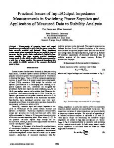
Current-mode filters with high output impedance and employing only grounded components SUDHANSHU MAHESHWARI Department of Electronics Engineering, Z. H. College of Engineering and Technology, A.M.U., Aligarh 202 002, INDIA. E-mail:
[email protected]
Abstract: This paper presents several new current-mode second order filters suited for low-Q applications. The new circuits employ only grounded components and possess high output impedance, ideal for current-mode cascading. Effects of non-idealities and parasitics are also discussed. The new circuits possess good active and passive sensitivity performance. PSPICE simulation results are included for verification of proposed circuits. Keywords: Current-mode, analog signal processing, active filter, differential voltage current conveyor the drawback of using matching conditions for realizing two functions [15]. This paper presents several second order low-Q current mode filter circuits employing grounded components and with high output impedance. LowQ filters find applications, for instance in antialiasing, graphic equalizers etc [8, 17]. Moreover the circuits using grounded components are beneficial from fabrication viewpoint. The non-ideal study and parasitic effects are also given. The new circuits are verified using PSPICE, a powerful tool for verifying new circuits based on active elements, which are either not commercially available or their implementation using available ICs is not very economical.
1 Introduction Current-mode circuits have become quite popular for their potential advantages over the voltage-mode counterparts [1-3]. Current-mode analog signal filtering has also received a lot of attention in the recent past. The technical literature has thus been flooded with numerous new circuit realizations [418]. Current-mode filters with high output impedance offer easy cascading and are quite desirable for realizing higher order filters as well. Recently CDTA has also been used for currentmode filtering application [5]. The circuit of ref. [6] realizes three basic filtering functions at high output impedance and uses all grounded components. The circuit in ref. [7] is based on minimum number of passive elements. Another current mode work employs only one active element in form of a CFOA [8]. One multifunction filter using two CDBAs was also reported [9]. Current mode universal filter of ref. [12] falls in a separate category of electronically tunable filters and also benefits from cascadable outputs and use of grounded components. An active element which has also emerged as a potential candidate for realizing filter circuits is differential voltage current conveyor [10-11, 13-16]. The works based on DVCC present a KHN biquad [10] and higher order low-pass filters [11] both benefiting from high output impedance outputs. Another very recent current-mode work also enjoys the use of only grounded components and high output impedance [15]. However, the work requires input current insertion at different nodes for realizing different functions. In some cases, additional active elements are required for making multiple copy of input current. Moreover, the work also suffers from
ISSN: 1109-9445
2 Proposed Circuits The differential voltage current conveyor (DVCC) is characterized by the following port relationship [14] Vx = VY1-VY2; IY1 = IY2 = 0; IZ+ = Ix; IZ- = -Ix
(1)
The new proposed current-mode filter circuits are shown in Fig. 1. The new circuits are derived using the cascade approach, from the first order filters recently reported in literature [13]. The same are shown here as Fig. 2 for easy reference [13]. Circuit analysis using eqn. (1) yields the following current transfer functions for the circuits of Fig. 1. 2 Fig. 1(a): I o = s . (2a) I in D( s ) (2b) Fig. 1(b): I o = 1 / 4 R1 R2C1C 2 . I in D( s) (2c) Fig. 1(c): I o = − s / 2 R2C2 . I in D(s)
238
Issue 6, Volume 5, June 2008
WSEAS TRANSACTIONS on ELECTRONICS
Sudhanshu Maheshwari
Fig. 1(d): I o s 2 − s(1 / 2 R1C1 + 1 / 2 R2C2 ) + 1 / 4 R1 R2C1C2 . = I in D( s ) 2 Fig. 1(e): I o = 2( s + 1 / 4 R1 R2C1C2 ) ,
I in
Iin (2d) Y2 Y1 DVCC(1)
(2e)
D( s)
X
where D(s) = s2 + s(1/ 2R1C1 +1/ 2R2C2 ) +1/ 4R1R2C1C2
Pole frequency ωo =1/ 2 R1R2C1C2 Bandwidth ωo / Q = (1/ 2R1C1 +1/ 2R2C2 ) R1R2C1C2
Quality factor Q =
2(R1C1 + R2C2 )
Z-
C1
R1
(3)
It is seen from eqn. (2) that high-pass (HP), lowpass (LP), band-pass (BP), all-pass (AP) and bandreject (BR) filter functions are realized from the circuits of Figure 1 (a-e) respectively. It may be noted that BR and AP realization requires additional current followers (like the recent work of ref. 15) to duplicate the input current and finite current transfer gain (α) would cause for some non-ideality. The filter gains, pole-frequency and quality factor are found as:
Gains: HHP=HLP=HAP=1; HBR=2; HBP=-R1C1/(R1C1+R2C2)
Z+
Y2 Y1 DVCC(2) X
Z+
Z-
C2
R2 Io
Fig. 1b: Proposed low-pass filter
(4)
Iin
(5) (6)
Y2 Y1 DVCC(1)
(7)
X
Iin
Z+
Z-
C1
R1 Y2 Y1 DVCC(1) X
Z+
Z-
Y2 Y1 DVCC(2)
C1
R1
X
Z+
C2
R2 Io
Y2 Y1 DVCC(2) X
Z+
Fig. 1c: Proposed band-pass filter.
Z-
It is evident from eqns. (5-7) that the proposed circuits have low-Q capability. But it is not to be seen as a drawback, because of the simplicity of the realization approach, the circuit structure, along with the high output impedance feature. The sensitivity of pole-frequency and pole-Q to passive
C2
R2 Io
Fig. 1a: Proposed high-pass filter.
ISSN: 1109-9445
Z-
239
Issue 6, Volume 5, June 2008
WSEAS TRANSACTIONS on ELECTRONICS
Sudhanshu Maheshwari
components is within 0.5 in magnitude and becomes ‘0’ for equal valued resistor and capacitor design. Thus the proposed circuits exhibit good sensitivity performance.
It is further to be noted that the circuits of Fig. 1(ac) are based on DVCC with both Z+ and Z- outputs, but the all-pass and band-reject filters of Fig. 1 (d and e respectively) employ one of the two DVCCs with an additional Z+ stage. This is easily incorporated by using two additional steering transistors to implement an additional Z+ output in the DVCC implementation [13].
Iin
Iin Y2
Y1 DVCC(1)
X
Iin
Z+ Z+ Z-
Y2 Y1 DVCC
C1
R1
X
Z+
Z-
C
R Io Y2 Y1 DVCC(2) X
Z+
Io 1 / 2 RC = I in s + 1 / 2 RC
(a)
Z-
Iin
C2
R2
Y2 Y1 DVCC
Io
X
Fig. 1d: Proposed all-pass filter.
Z-
C
R
Iin
Iin
Z+
Io Y2
Y1 DVCC(1)
X
(b)
Z+ Z+ Z-
Io −s = I in s + 1 / 2 RC
Iin
Iin
C1
R1
Y2 Y1 DVCC X Y2 Y1 DVCC(2) X
Z+
R2
Z-
C
R Io
Z-
Iin
C2
(c)
Io
Io s − 1 / 2 RC =− I in s + 1 / 2 RC
Fig. 2: First order (a) Low-pass, (b) High-pass, and (c) All-pass building blocks used in the biquads filters of Fig. 1 [13].
Fig. 1e: Proposed band-reject filter.
ISSN: 1109-9445
Z+
240
Issue 6, Volume 5, June 2008
WSEAS TRANSACTIONS on ELECTRONICS
Sudhanshu Maheshwari
resistors, the transfer functions actually get modified by way of an additional high frequency root. But again as this root lies at very high frequencies (since parasitic capacitance is in order of pF’s and external resistor is also within a few Kohms), their effects do not get noticeable at working frequencies.
3 Non-ideal study 3.1
DVCC non-idealities
The non-ideal DVCC is characterized by the following relationship. Vx=β1Vy1-β2Vy2; Iy1=Iy2=0; Iz+=α1Ix; Iz-=-α2Ix
(8)
The voltage transfer gains β1 from Y1 to X, and β2 from Y2 to X deviate from unity by voltage transfer errors. Similarly, the current transfer gains α1 from X to Z+ and α2 from X to Z- deviate from unity by the current transfer errors [13]. These errors are expected to be quite low for an integrated DVCC, thus making voltage and current transfer gains to approach unity. The first three circuits of Figure 1 are re-analyzed using eqn. (8) to yield the following non-ideal current transfer functions. I o α 11α 12 s 2 Fig .1(a) :
I in
=
D( s )
Fig .1(b) :
I o α 11α 12 β 11 β 12 / 4 R1 R 2 C1C 2 = I in D( s )
Fig .1(c) :
Io α α β s / 2R2 C 2 = − 11 12 12 I in D( s )
4 Simulation results The new proposed circuits are verified through PSPICE simulations. The DVCC was simulated using the parameters as listed recent ref. [13]. The supply voltage used was ±2.5V. The circuits were designed with equal value capacitors of value 1nF, and equal resistors of value 1KΩ. The designed pole-frequency is 80 KHz and pole-Q is 0.5. The simulation results are shown in Figure 3-5. Figures 3-5 respectively shows the band-pass, band-reject and all-pass responses. The pole-frequency in each case is found to be 80 KHz, which matches the designed value. Next, the time domain responses for all-pass circuit are shown with input signal at polefrequency. The input and output waveforms (Figure 6) are out of phase as desired for second order allpass function at pole-frequency. Figure 7 shows the input/output waveforms at 1.8MHz, where the phase-shift becomes -360º, thus confirming circuit’s performance even at high frequencies.
(9a)
(9b) (9c )
where D(s) = s2 + s(α21β11/ 2R1C1 +α22β12/ 2R2C2)+α21α22β11β12 / 4R1R2C1C2 (10)
0
Similar results are obtained for the all-pass and band-reject, as theses are only derived from the above. The sensitivity of filter parameters to the current and voltage transfer gains are analyzed and found within 0.5 in magnitude which suggests good sensitivity performance. It is to be noted that the current and voltage transfer gains are frequency dependent, with a first order roll-off. These are however, found to be unity up to 10’s of MHz and the exact value may vary for different technology and device dimensions.
-10
-20
-30
-40
-50 1.0KHz IDB(VO)
10KHz
30KHz
100KHz
300KHz
1.0MHz
3.0MHz
10MHz
Frequency
Fig. 3: Band-pass response.
3.2 DVCC Parasitics
0
Next, the effects of various parasitic capacitances are to be considered. It was recently shown that these parasitics do not adversely affect the basic circuit topology used in this work [13]. However, it is worth to be noted that parasitic capacitances at various ports do cause some concern. For instance, in all the proposed circuits, the port parasitic capacitances either merge with external capacitors or appear in shunt with external resistors. In the former case, since the external capacitors chosen in design are in excess to the expected parasitic capacitances, their effect is not noticeable. In the latter case, where these appear in shunt with external
ISSN: 1109-9445
3.0KHz
-20 SEL>> -40 IDB(VO2) 100d
0d
-100d 100Hz IP(VO2)
1.0KHz
10KHz
100KHz
1.0MHz
10MHz
Frequency
Fig. 4: Band-reject gain and phase response.
241
Issue 6, Volume 5, June 2008
WSEAS TRANSACTIONS on ELECTRONICS
Sudhanshu Maheshwari
20uA
5 Conclusion New current-mode second order filters, each using only two DVCCs and grounded passive components suited for low-Q (≤0.5) applications are proposed. The five new circuits realize all the standard second order filter functions at high output impedance. The new circuits are based on the recently reported first order filters [13]. The proposed circuits require no matching conditions for realizing any filtering function, unlike a recent work based on equal number of active and passive components [15]. The circuits also possess good sensitivity performance. Effects of DVCC non-idealities and parasitics are also discussed. PSPICE simulation results confirm the practical utility of the proposed circuits. Current-mode applications of DVCC continue to find recent attention in technical literature [19].
0A
-20uA I(iin1) 20uA
0A
SEL>> -20uA 2.0us I(vo)
2.5us
3.0us
3.5us
4.0us
Time
Fig. 7: Input/Output of all-pass filter at 1.8MHz.
Acknowledgements: The author is thankful to the anonymous reviewers for useful comments. The author is also grateful to the guest editors for recommending the paper.
10 5 0 -5
References:
-10 idb(vo) 0d -100d
[1] G. W. Roberts and A. S. Sedra, All currentmode frequency selective circuits, Electronics Letters, vol. 25, 1989, pp. 759-761. [2] B. Wilson, Recent developments in current conveyors and current-mode circuits, IEE Proc. G, vol. 132, 1990, pp. 63-76. [3] C. Toumazou, F. J. Lidgey, D. G. Haigh, Analogue IC design: the current-mode approach, IEE, U.K, 1998. [4] A. M. Soliman, Current-mode universal filter, Electron Letts., vol. 32, 1995, pp. 1420-1421. [5] D. Biolek, V. Biolkova, Three CDTA currentmode biquad, WSEAS Trans Circuits Syst, vol. 4, 2005, pp. 1227-1232 [6] M. T. Abuelma’atti, M. H. Khan, Low component current-mode universal filter, Electron Letts., vol. 31, 1995, pp. 2160-2161. [7] O. Cicekoglu, Current mode biquad with a minimum number of passive elements, IEEE Trans CAS-II, vol. 48, 2001, pp. 221-222. [8] R. K. Sharma, R. Senani, Universal current mode biquad using a single CFOA, Int J Elec., vol. 91, 2004, pp. 175-183. [9] A. U. Keskin, E. Hancioglu, Current mode multifunction filter using two CDBAs, Int J Electr. Commn,(AEU), vol. 59, 2005, pp. 495498. [10] M. A. Ibrahim, S. Minaei, H. Kuntman, A 22.5MHz current mode KHN biquad using
-200d -300d SEL>> -400d 100Hz ip(vo)
1.0KHz
10KHz
100KHz
1.0MHz
10MHz
Frequency
Fig. 5: All-pass gain and phase response. 30uA
20uA
0A
-20uA
-30uA 0s I(iin1)
5us I(vo)
10us
15us
20us
25us
30us
Time
Fig. 6: Input/output of all-pass filter at polefrequency (80KHz).
ISSN: 1109-9445
242
Issue 6, Volume 5, June 2008
WSEAS TRANSACTIONS on ELECTRONICS
Sudhanshu Maheshwari
differential voltage current conveyor, Int J Electr. Commn,(AEU), vol. 59, 2005, pp. 311318. [11] J. Cajka, T. Dostal, K. Vrba, High order lowpass filters using DVCC elements, Radioengineering, vol. 11, 2002, pp. 14-17. [12] S. Maheshwari, I.A. Khan, High performance versatile translinear-C universal filter. Journal of Active and Passive Electronic Devices, vol. 1, 2005, pp. 41-51. [13] S. Maheshwari, High output impedance current mode all-pass sections with two grounded passive components, IET: Circuits Devices and Systems, vol. 2, 2008, pp. 234-242. [14] H. O. Elwan and A. M. Soliman, Novel CMOS differential voltage current conveyor and its applications, IEE Proc., Circuits Devices Syst., vol. 144, 1997, pp. 195–200.
ISSN: 1109-9445
[15] T. Tsukutani, Y. Sumi, N. Yabuki, Novel current mode biquadratic circuits using only plus type DO-DVCCs and grounded passive components, Int J Elect., vol. 94, 2007, pp. 1137-1146. [16] S. Maheshwari, A canonical voltage controlled VM-APS a grounded capacitor, Circuits Systems and Signal Processing, vol. 27, 2008, pp. 123-132. [17] G. W. Roberts and A. S. Sedra, A general class of current amplifier based biquadratic filter circuits, IEEE Trans CAS-I, vol. 39, 1992, pp. 257-263. [18] A. M. Soliman, Current conveyor filters: Classification and review, Microelectronic Journal, vol. 29, 1998, pp. 133-149. [19] S. Maheshwari, Novel cascadable current mode first order all-pass sections, Int J Elect., vol. 94, 2007, pp. 995-1003.
243
Issue 6, Volume 5, June 2008