ECE-C 490/690 ST: Custom VLSI Design. Syllabus. Fall 2009. Lec: Mon ... S. M.
Kang and Y. Leblebici, CMOS Digital Integrated Circuits. Analysis & Design ...
ECE-C 490/690 ST: Custom VLSI Design Fall 2009 Prof. Baris Taskin
Syllabus Lec: Mon 10:00-11:50am Lab: Wed 9:00am-10:50am
Course Information Course Title: Course Type: Credits: Duration:
ST: Custom VLSI Design Undergraduate/Graduate cross listing 3 credits Fall Quarter
Audience This course is intended for senior-level ECE undergraduate students and graduate students. Workload for graduate and undergraduate students will be different and two parties will be evaluated independently.
Prerequisites Knowledge of digital logic design (ECE 200) and introductory electronics (ECE-L 301-302) is required. Previous exposure to transistors and semiconductor devices would be useful but not required. These introductory topics will be discussed in early stages of the course to provide necessary technical background to all students from EE and CE.
Course Description This is an introductory course in the field of Very Large Scale Integration (VLSI) circuit and systems design. Systematic understanding, design and analysis of VLSI integrated circuits will be covered. This course will focus exclusively on digital CMOS VLSI circuit and systems design, although some issues in mixed-signal mode will also be addressed. The course will begin with a review of CMOS transistor operation and semiconductor manufacturing process. Logic design with CMOS transistors and circuit families will be described. Specifically, layout, design rules, and circuit simulation will be addressed towards the coverage of custom VLSI design principles. Course objectives include: • To learn the basic concepts of modern VLSI circuit design by studying logic design, physical structure and fabrication of semiconductor devices and how they are combined to build systems for efficient data processing, • To learn the interface of logic and electronics through analyzing electrical and design characteristics of transistors and gates for high-performance integrated circuits, • To understand the role of computer-aided design (CAD) tools in automating the design flow and providing improved productivity in VLSI systems design, • To understand the relationship between semiconductor technology, transistors and architecture, addressing all levels of hierarchy in VLSI system design flow.
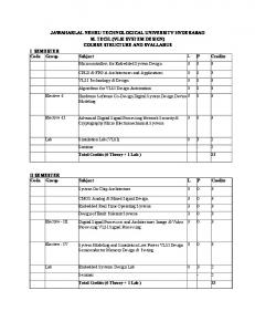
1
Course Structure Laboratory: Exam(s): Homework(s): Project(s):
Once a week for 1 hour, six (6) assignments One (1) final examination. Two (2) homeworks will be assigned. None
This is a senior level undergraduate level/graduate level class and the evaluation criteria is established accordingly. The evaluation process will encompass the monitoring of not the quality of individual work but also participation in group projects and lectures. The final grade will be calculated as follows: Final Homework(s) Lab assignment(s) Total
→ → →
30% 20% 50% 100%
Note that this course is cross-listed as a graduate level course. Graduate and undergraduate course work will be different and students will be evaluated independently. Graduate students will have more questions on the homeworks and examinations.
Textbook Following is a list of suggested textbooks for this course, starting with the required textbook by J. M. Rabaey, A. Chandrakasan and B. Nikolic. The additional textbooks 1 through 3 provide much additional information and can be quite useful. Required Textbook:
J. M. Rabaey, A. Chandrakasan and B. Nikolic, Digital Integrated Circuits, Prentice Hall, 2nd edition, 2003, ISBN:0130909963.
Additional Reading:
1. N. H. Weste and D. Harris, CMOS VLSI Design: A Circuits and Systems Perspective, Addison-Wesley, 2nd ed., 2004. 2. John P. Uyemura, Introduction to VLSI Circuits and Systems: A Design Perspective, Prentice-Hall, Inc., 2002. 3. S. M. Kang and Y. Leblebici, CMOS Digital Integrated Circuits Analysis & Design, McGraw-Hill Inc., 2002.
Laboratory Weekly design and simulation assignments using Cadence CAD tools. Specifically, Cadence Virtuoso tool for layout, Analog Artist using simulators Spice and Spectre for simulation and Diva/Accura for DRC will be used. Weekly assignments will include: • CMOS Inverter
• CMOS NAND and NOR gates • XOR and MUX gates
• Learning about data paths: A simple sequential circuit (i.e. 2-bit adder with storage) 2
Tentative Schedule Week 1 2 3 4 5 6 7 8 9 10 11 12
Lecture Introduction to VLSI Systems CMOS Fabrication The Devices: NMOS and PMOS The Wire Static CMOS Inverter: Speed, Area, Scaling Static CMOS Inverter and Layout Techniques CMOS Design Techniques Logical Effort Static CMOS Dynamic CMOS Sequential Logic 1: Registers Sequential Logic 2: Clock, Timing Final Examination (Date TBA)
3
Chapter 1 2 3 4 5 5 6 6 6.2 6.3 7 7
Lab
CMOS inverter design CMOS NAND and NOR Inverter Chain HW #1 CMOS XOR and MUX 2-bit Adder HW #2 D Latch and DFF