Data Processing on FPGAs Rene Mueller
[email protected]
Jens Teubner
[email protected]
Gustavo Alonso
[email protected]
Systems Group, Department of Computer Science, ETH Zurich, Switzerland
ABSTRACT Computer architectures are quickly changing toward heterogeneous many-core systems. Such a trend opens up interesting opportunities but also raises immense challenges since the efficient use of heterogeneous many-core systems is not a trivial problem. In this paper, we explore how to program data processing operators on top of field-programmable gate arrays (FPGAs). FPGAs are very versatile in terms of how they can be used and can also be added as additional processing units in standard CPU sockets. In the paper, we study how data processing can be accelerated using an FPGA. Our results indicate that efficient usage of FPGAs involves non-trivial aspects such as having the right computation model (an asynchronous sorting network in this case); a careful implementation that balances all the design constraints in an FPGA; and the proper integration strategy to link the FPGA to the rest of the system. Once these issues are properly addressed, our experiments show that FPGAs exhibit performance figures competitive with those of modern general-purpose CPUs while offering significant advantages in terms of power consumption and parallel stream evaluation.
1.
INTRODUCTION
Taking advantage of specialized hardware has a long tradition in data processing. Some of the earliest efforts involved building entire machines tailored to database engines [8]. More recently, graphic processing units (GPUs) have been used to efficiently implement certain types of operators [11, 12]. Parallel to these developments, computer architectures are quickly evolving toward heterogeneous many-core systems. These systems will soon have a (large) number of processors and the processors will not be identical. Some will have full instruction sets, others will have reduced or specialized instruction sets; they may use different clock frequencies or exhibit different power consumption; floating point arithmetic-logic units will not be present in all proces-
Permission to copy without fee all or part of this material is granted provided that the copies are not made or distributed for direct commercial advantage, the VLDB copyright notice and the title of the publication and its date appear, and notice is given that copying is by permission of the Very Large Data Base Endowment. To copy otherwise, or to republish, to post on servers or to redistribute to lists, requires a fee and/or special permission from the publisher, ACM. VLDB ‘09, August 24-28, 2009, Lyon, France Copyright 2009 VLDB Endowment, ACM 000-0-00000-000-0/00/00.
sors; and there will be highly specialized cores such as fieldprogrammable gate arrays (FPGAs) [13, 22]. An example of such a heterogeneous system is the Cell Broadband Engine, which contains, in addition to a general-purpose core, multiple special execution cores (synergistic processing elements, or SPEs). Given that existing applications and operating systems already have significant problems when dealing with multicore systems [5], such diversity adds yet another dimension to the complex task of adapting data processing software to new hardware platforms. Unlike in the past, it is no longer just a question of taking advantage of specialized hardware, but a question of adapting to new, inescapable architectures. In this paper, we focus our attention on FPGAs as one of the more different elements that can be found in manycore systems. FPGAs are (re-)programmable hardware that can be tailored to almost any application. However, it is as yet unclear how the potential of FPGAs can be efficiently exploited. Our contribution with this work is to study the design trade-offs encountered when using FPGAs for data processing, as well as to provide a set of guidelines for how to make design choices such as: (1) FPGAs have relatively low clock frequencies. Na¨ıve designs will exhibit a large latency and low throughput. We show how this can be avoided by using asynchronous circuits. We also show that asynchronous circuits (such as sorting networks) are well suited for common data processing operations like comparisons and sorting. (2) Asynchronous circuits are notoriously more difficult to design than synchronous ones. This has led to a preference for synchronous circuits in studies of FPGA usage [13]. Using the example of sorting networks, we illustrate systematic design guidelines to create asynchronous circuits that solve database problems. (3) FPGAs provide inherent parallelism whose only limitation is the amount of chip space to accommodate parallel functionality. We show how this can be managed and demonstrate an efficient circuit for parallel stream processing. (4) FPGAs can be very useful as database co-processors attached to an engine running on conventional CPUs. This integration is not trivial and opens up several questions on how an FPGA can fit into the complete architecture. In our work, we demonstrate an embedded heterogeneous multi-core setup and identify trade-offs in FPGA integration design.
(5) FPGAs are attractive co-processors because of the potential for tailored design and parallelism. We show that FPGAs are also very interesting in regard to power consumption as they consume significantly less power, yet provide at a performance comparable to the one of conventional CPUs. This makes FPGAs good candidates for multi-core systems as cores where certain data processing tasks can be offloaded. To illustrate the trade-offs and as a running example, we describe the implementation of a median operator that depends on sorting as well as on arithmetics. We use it in a streaming fashion to illustrate sliding window functionality. The implementation we discuss in the paper is designed to illustrate the design space of FPGA-based co-processing. Our experiments show that FPGAs can clearly be a useful component of a modern data processing system, especially in the context of multi-core architectures. Outline. We start our work by setting the context with related work (Section 2). After introducing the necessary technical background in Section 3, we illustrate the implementation of a median operator using FPGA hardware (Section 4). Its integration into a complete multi-core system is our topic for Section 5, before we evaluate our work in Section 6. We wrap up in Section 7.
2.
RELATED WORK
A number of research efforts have explored how databases can use the potential of modern hardware architectures. Examples include optimizations for cache efficiency (e.g., [21]) or the use of vector primitives (“SIMD instructions”) in database algorithms [29]. The QPipe [14] engine exploits multi-core functionality by building an operator pipeline over multiple CPU cores. Likewise, stream processors such as Aurora [2] or Borealis [1] are implemented as networks of stream operators. An FPGA with database functionality could directly be plugged into such systems to act as a node of the operator network. The shift toward an increasing heterogeneity is already visible in terms of tailor-made graphics or network CPUs, which have found their way into commodity systems. Govindaraju et al. demonstrated how the parallelism built into graphics processing units can be used to accelerate common database tasks, such as the evaluation of predicates and aggregates [12]. The GPUTeraSort algorithm [11] parallelizes a sorting problem over multiple hardware shading units on the GPU. Within each unit, it achieves parallelization by using SIMD operations on the GPU processors. The AASort [17], CellSort [9], and MergeSort [6] algorithms are very similar in nature, but target the SIMD instruction sets of the PowerPC 970MP, Cell, and Intel Core 2 Quad processors, respectively. The use of network processors for database processing was studied by Gold et al. [10]. The particular benefit of such processors for database processing is their enhanced support for multi-threading. We share our view on the role of FPGAs in upcoming system architectures with projects such as Kiwi [13] or Liquid Metal [15]. Both projects aim at off-loading traditional CPU tasks to programmable hardware. Mitra et al. [22] recently outlined how FPGAs can be used as co-processors in an SGI Altix supercomputer to accelerate XML filtering.
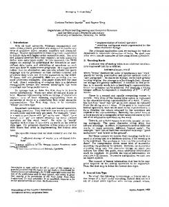
CLB slice switch box PPC core 0
PPC core 1
BRAM 18x18bit multiplier
Figure 1: Simplified FPGA architecture: 2D array of CLBs, each consisting of 4 slices and a switch box. Available in silicon: 2 PowerPC cores, BRAM blocks and multipliers. The advantage of using customized hardware as a database co-processor is well known since many years. For instance, DeWitt’s direct system comprises of a number of query processors whose instruction sets embrace common database tasks such as join or aggregate operators [8]. Similar ideas have been commercialized recently in terms of database appliances sold by, e.g., Netezza [7], Kickfire [19], or XtremeData [16]. All of them appear to be based on specialized, hard-wired acceleration chips, which primarily provide a high degree of data parallelism. Our approach can be used to exploit the reconfigurability of FPGAs at runtime. By reprogramming the chip for individual workloads or queries, we can achieve higher resource utilization and implement data and task parallelism. By studying the foundations of FPGA-assisted database processing in detail, this work is an important step toward our goal of building such a system. FPGAs are being successfully applied in signal processing, and we draw on some of that work in Sections 4 and 5. The particular operator that we use as a running example to demonstrate FPGA-based co-processing is a median over a sliding window. The implementation of a median with FPGAs has already been studied [27], but only on smaller values than the 32 bit integers considered in this paper. Our median implementation is similar to the sorting network proposed by Oflazer [24]. As we show in Section 6.1, we gain significant performance advantages by designing the network to run in an asynchronous mode.
3.
OVERVIEW OF FPGAS
Field-programmable gate arrays are reprogrammable hardware chips for digital logic. FPGAs are an array of logic gates that can be configured to construct arbitrary digital circuits. These circuits are specified using either circuit schematics or hardware description languages such as Verilog or VHDL. A logic design on an FPGA is also referred to as a soft IP-core (intellectual property core). Existing commercial libraries provide a wide range of pre-designed cores, including those of complete CPUs. More than one soft IP-core can be placed onto an FPGA chip.
3.1
FPGA Architecture
Figure 1 sketches the architecture of the Xilinx Virtex II Pro XC2VP30 FPGA used in this paper [28]. The FPGA is
PowerPC cores Slices 18 kbit BRAM blocks 18×18-bit multipliers I/O pads
3.2
2 13,696 136 (=2,448 kbit, usable as 272 kB) 136 644
Table 1: Characteristics of Xilinx XC2VP30 FPGA. carryout Y DY
MUXCY 0
1
G4
D
G3 D
Q
YQ
Hardware Setup
FPGAs are typically available pre-mounted on a circuit board that includes additional peripherals. Such circuit boards provide an ideal basis for the assessment we perform here. Quantitative statements in this report are based on a Xilinx XUPV2P development board with a Virtex-II Pro XC2VP30 FPGA chip. Relevant for the discussion in this paper are the DDR DIMM socket which we populated with a 512 MB RAM module. For terminal I/O of the software running on the PowerPC, a RS232 UART interface is available. The board also includes a 100 Mbit Ethernet port. The board is clocked at 100 MHz. This clock drives both, the FPGA-internal buses as well as the external I/O connectors, such as the DDR RAM. The PowerPC cores are clocked at 300 MHz.
G2 G1 LUT
4.
Register/ Latch
& 0 MUXCY
1 0
F4
D
D
F3
Y DY
1
Q
YQ
F2 F1 LUT
Register/ Latch
& 0 1
carryin
Figure 2: Simplified Virtex-II Pro slice consisting of 2 LUTs and 2 register/latch components. The gray components are configured during programming.
a 2D array of configurable logic blocks (CLBs). Each logic block consists of 4 slices that contain logic gates (in terms of lookup tables, see below) and a switch box that connects slices to an FPGA interconnect fabric. In addition to the CLBs, FPGA manufacturers provide frequently-used functionality as discrete silicon components (hard IP-cores). Such hard IP-cores include block RAM (BRAM) elements (each containing 18 kbit fast storage) as well as 18×18-bit multiplier units. A number of Input/Output Blocks (IOBs) link to external RAM or networking devices. Two on-chip PowerPC 405 cores are directly wired to the FPGA fabric and to the BRAM components. Table 1 shows a summary of the characteristics of the FPGA used in this paper. A simplified circuit diagram of a programmable slice is shown in Figure 2. Each slice contains two lookup tables (LUTs) with four inputs and one output each. A LUT can implement any binary-valued function with four binaryinputs. The output of the LUTs can be fed to a buffer block which can be configured as a register (flip-flop). The output is also fed to a multiplexer (MUXCY in Figure 2), which allows the implementation of fast carry logic.
A STREAMING MEDIAN OPERATOR
As a running example suitable to illustrate the design of data processing operations in FPGAs, we have implemented an operator that covers many of the typical aspects of data intensive operations such as comparisons of data elements, sorting, and I/O issues. In this way the lessons learned from implementing this operator can be generalized to other operators using similar building blocks. The design illustrates many of the design constraints in FPGAs, which are very different from the design constraints encountered in conventional database engines. For instance, parallelism in a normal database is limited by the CPU and memory available. In an FPGA, it is limited by the chip space available. In a CPU, parallel threads may interfere with each other. In an FPGA, parallel circuits do not interfere at all, thereby achieving 100 % parallelism. Similarly, algorithms in a CPU look very different from the same algorithms implemented as circuits and, in fact, they have very different behavior and complexity patterns. We illustrate many of these design aspects using a median operator over a count-based sliding window implemented on the aforementioned Xilinx board. This is an operator commonly used to, for instance, eliminate noise in sensor readings [25] and in data analysis tasks [26]. For illustration purposes and to simplify the figures and the discussion, we assume a window size of 8 tuples. For an input stream S, the operator can then be described in CQL [3] as Select median(v) From S [ Rows 8 ] .
(Q1 )
The semantics of this query are illustrated in Figure 3. Attribute values vi in input stream S are used to construct a new output tuple Ti0 for every arriving input tuple Ti . A conventional (CPU-based) implementation would probably use a ring buffer to keep the last eight input values (we assume unsigned integer numbers), then, for each input tuple Ti , (1) sort the window elements vi−7 , . . . , vi to obtain an ordered list of values v10 ≤ · · · ≤ v80 and v 0 +v 0
(2) compute the mean value between v40 and v50 , 4 2 5 , to construct the output tuple Ti0 (for an odd-sized window, the median would instead be the middle element of the sorted sequence). We will shortly see how the data flow in Figure 3 directly
T9
T8 T7 T6 T5
T4 T3
T2 T1 T0 input stream
t
count−based window v9 v8 v7 v6 v5 v4 v3 v2
v1
sorting v’1 v’2 v’3 v’4 v’5 v’6 v’7 v’8 + :2 T’ 9 T’9 t
T’ 8 T’ 7 T’ 6 T’ 5
streaming median operator T’ 4 T’ 3 T’ 2 T’ 1 T’ 0
output stream
Figure 3: Median aggregate over a count-based sliding window (window size 8).
leads to an implementation in FPGA hardware. Before that, we discuss the algorithmic part of the problem for Step (1).
4.1
Sorting
Sorting is the critical piece in the median operator and known to be particularly expensive on conventional CPUs. It is also a common data processing operation that can be very efficiently implemented in FPGAs using asynchronous circuits. Highly tuned and vectorized software implementations require in the order of fifty cycles to sort eight numbers on modern CPUs [6]. Sorting Networks. Some of the most efficient conventional approaches to sorting are also the best options in the context of FPGAs. Sorting networks are attractive in both scenarios, because they (i) do not require control flow instructions or branches and (ii) are straightforward to parallelize (because of their simple data flow pattern). On modern CPUs, sorting networks suggest the use of vector primitives, which has been demonstrated in [9, 11, 17]. Figure 4 illustrates two different networks that sort eight input values. Input data enters a network at the left end. As the data travels to the right, comparators each exchange two values, if necessary, to ensure that the larger value always leaves a comparator at the bottom. The bitonic merge network (Figure 4(a)) is based on a special property of bitonic sequences (i.e., those that can be obtained by concatenating two monotonic sequences). A component-wise merging of two such sequences always yields another bitonic sequence, which is efficiently brought into monotonic (i.e., sorted) order afterward. In an even-odd merge sorting network (Figure 4(b)), an input of 2p values is split into two sub-sequences of length 2p−1 . After the two 2p−1 -sized sequences have been sorted (recursively using even-odd merge sorting), an even-odd merger combines them into a sorted result sequence. Other sorting algorithms can be represented as sorting networks, too. For details we refer to the work of Batcher [4] or a textbook
[20]. Sorting Network Properties. As can be seen in the two example networks in Figure 4, the number of comparisons required for a full network implementation depends on the particular choice of the network. The bitonic merge sorter for N = 8 inputs in Figure 4(a) uses 24 comparators in total, whereas the even-odd merge network (Figure 4(b)) can do with only 19. For other choices of N , we listed the required number of comparators in Table 2. The graphical representation in Figure 4 indicates another important metric of sorting networks. Comparators with independent data paths can be grouped into processing stages and evaluated in parallel. The number of necessary stages is referred to as the depth S(N ) of the sorting network. For eight input values, bitonic merge networks and even-odd merge networks both have a depth of six. Compared to even-odd merge networks, bitonic merge networks observe two additional interesting characteristics: (i) all signal paths have the same length (by contrast, the data path from x0 to y0 in Figure 4(b) passes through three comparators, whereas from x5 to y5 involves six) and (ii) the number of comparators in each stage is constant (4 comparators per stage for the bitonic merge network, compared with 2–5 for the even-odd merge network). CPU-Based Implementations. These two properties are the main reason why many software implementations of sorting have opted for a bitonic merge network, despite its higher comparator count (e.g., [9, 11]). Differences in path lengths may require explicit buffering for those values that do not actively participate in comparisons at specific processing stages. At the same time, additional comparators might cause no additional cost in architectures that can evaluate a number of comparisons in parallel using, for instance, the SIMD instruction sets of modern CPUs.
4.2
An FPGA Median Operator
Once the element for sorting is implemented using a sorting network, the complete operator can be implemented in an FPGA using the sketch in Figure 3. Each of the solid arrows corresponds to 32 wires in the FPGA interconnect fabric, carrying the binary representation of a 32-bit integer number. Sorting and mean computation can both be packaged into logic components, whose internals we now present. Comparator Implementation on an FPGA. The data flow in the horizontal direction of Figure 4 also translates into wires on the FPGA chip. The entire network is obtained by wiring a set of comparators, each implemented in FPGA logic. The semantics of a comparator is easily expressible in the hardware description language VHDL (where