Jan 4, 1979 - United States Patent [191. Steigmeier et ... U.S. PATENT DOCUMENTS ... CIRCUIT l0 OPTIC SYSTEM. 60. POLARIZER PR. [x. PROCESSING.
United States Patent [191
[11] [45]
Steigmeier et al. [54] DEFECT DETECTION SYSTEM [75] Inventors: Edgar F. Steigmeier, Hedingen; Karl
19782
Surface Detects on Silicon Wafers by Scattered Light
Primary Examiner—John K. Corbin
[73] Assignee: RCA Corporation, New York, NY. [21] App]. No.: 813
Assistant Examiner-Bruce Y. Arnold Attorney, Agent, or Firm-—Samuel Cohen; H.
Christoffersen; William Squire
Jan. 4, 1979
[51]
Int. Cl.3 ........................................... .. GOlN 21/88
[52]
US. Cl. .................................. .. 356/237; 250/224;
[58]
Field of Search ............. .. 356/237, 240, 342, 445,
.
[57] ABSTRACT A laser beam projected through a prism in a direction normal to the surface of a circular wafer is focused into
356/342
a spot area and scanned along a spiral path on this sur
356/446-448, 337, 338; 350/63; 250/572, 224,
face. The focusing means comprises a relatively large aperture lens and the prism is on the lens axis. The retroreflected specular light passes through the lens and is prevented from reaching a light detector in the image plane of the lens by the prism. When the beam illumi nates a microscopic surface defect on the wafer, the light is diffracted and re?ected therefrom, and the lens captures that portion of the reflected light within the solid angle subtended by the lens, and passes that por tion thereof not blocked by the prism, to the light detec tor. The output of the detector may be employed to
203 CT; 358/342; 343/5 SC References Cited
[56]
Feb.
Measurements,” Semi-conductor, Silicon 1973.
Knop, Zurich, both of Switzerland
[22] Filed:
4,314,763
U.S. PATENT DOCUMENTS 2,913,568 11/1959
Kates ............................
3,176,306
Burns
3/1965
......
3,229,564
l/l966 Meltzer
3,561,876
2/1971
Hoffman .
3,565,568
2/1971
Hock
4,002,827 1/1977 4,128,834 12/1978
. . . . .. . . . .
250/225
. . . ..
250/572 X
356/448 X ....... .. 356/351 . . . ..
356/369
Nevin et al. ....... .. 358/140 Katagi ........................ .. 343/5 SCX
OTHER PUBLICATIONS
intensity modulate the beam of a cathode-ray tube dis
Conference on Laser and Electrooptical Systems, 7-9, Feb. 1978, OSA/IEE San Diego, Calif., pp. 90, 91, 92. Electronics, Mar. 16, 1978 pp. 48, 50. Patrick, W. J. and Patzner, E. J., “The Detection of
13 Claims, 6 Drawing Figures
play, the beam of which is spirally scanned in synchro nism with the scanning of the light beam.
CIRCUIT q
|
I
|
| |
r l0 OPTIC SYSTEM
i |
l I |
|
|
|
l l | l 1
60
POLARIZER PR
[x
PROCESSING CIRCUIT
54 2. 2
32 DISPLAY
U.S. Patent
Feb. 9, 1982
Sheet 3 of3
4,314,763
1
4,314,763
2
FIGS. 5 and 6 are graphs of'curves useful in illustrat
DEFECT DETECTION SYSTEM The present invention relates to an improved system
for optically detecting microscopic defects in a specu larly re?ecting surface of a given object and, more particulary, to such a system which is capable of deriv~ ing an image display of the spatial distribution of the locations of detected microscopic defects on the sur face. Silicon wafers, which are circular thin planar disks, are widely used in the manufacture of semi-conductor devices such as integrated circuits and the like. The slightest defects in the surface, such as dust particles too small to be seen with the naked eye, ?ngerprints, manu
facturing defects, and the like, are undesirable and should be detected as soon as possible in the manufac
turing process to reduce costs. Some presently available scan devices do not produce a display of such a defect pattern. Other systems that do produce such a display use rectangular scanning sys tems in which the beam is scanned along x-y rectangular coordinates. This is not suitable for circular objects. The edges of the objects are intercepted by the scan
beam and produce transient signals which interfere with the efficient operation of the instrument. Other systems collect a relatively small portion of diffracted light scattered from a microscopic defect and, therefore, have less than optimum sensitivity. An example of such a system is described in more detail in an article entitled, The Detection of Surface Defects on
Silicon Wafers by Scattered Light Measurements by W. J. Patrick and E. J. Patzner, Semi-Conductor, Silicon
1973, the Electro-Chemical Society, Inc., Princeton, N.J., 1973, pages 482-490. Other light scattering scan ning devices are described in articles by D. R. Oswald and D. F. Monroe, Journal of Electronic Materials 3, 225 (1974) and H. J. Ruiz, C. S. Williams and F. A.
Padovani, Journal of Electro-Chemical Society 121, 689 (1974). The system of the present invention, in contrast to those of the prior art, collects a large portion of all the
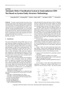
ing the present invention. In FIG. 1, system 10 includes a light source 16 which projects beam 12' through a series of prisms l8 and 20 and then through focusing means such as lens 22. The term light herein includes infrared, visible and ultravio let light. Light source 16 may be a low-power (such as l millivolt) laser, for example a He-Ne laser producing
light of 6328 angstroms wavelength which is focused by lens 22 into a spot 250 micrometers in diameter at 12.
This relatively small spot provides high resolution to the system. The beam 12 of laser light produced by lens 22 is projected onto the surface 14 of the unit under test (UUT), which may be a circular wafer of silicon as used
in the manufacture of integrated circuits and other semi conductor devices. The position ofthe light source 16 is not critical to the invention, but the position of the beam 12 between the prism 20 and the surface 14 is important. The axis of beam 12 should be perpendicular to the surface 14. The surface 14 of an acceptable wafer should be
smooth and plane. By surface is meant both the exposed surface and the underlying material to the depth at which the light may penetrate. In this case, the specular light that is re?ected from the planar surface 14 follows the path of beam 12, that is, it is retroreflected toward prism 20. Prism 20 acts as a spatial ?lter for the specu larly retrore?ected light along the axis of beam 12. Thus, any light retroreflected from an acceptable sur face, i.e. one that is normal to the axis of the beam 12, is incident on prism 20 and is not passed into detector 26.
The prism 20 is larger than beam 12 and; for example, may have sides which are i" by i". Should the position of the surface 14- being scanned have a defect therein, such as caused by dust particles, foreign matter, ?ngerprints, nicks, internal defects or the like which include those which are microscopic in
size having submicrometer dimensions, then such varia 40 tions in the surface will reflect and diffract the incident
beam 12 into a substantially broader pattern 24. The broader pattern 24 is co-axial with the beam 12 in the sense it may be dispersed 360° around the axis of beam 12, and the lens 22 collects a signi?cant portion of this
diffracted light scattered from a microscopic defect in the specularly reflecting surface of an object. More 45 broader pattern. This broader pattern provides im proved sensitivity to the present system. Lens 22 fo speci?cally, in accordance with the principles of the cuses the broader pattern 24 onto a high speed photodi present invention, the surface is scanned with an inci ode detector 26 which is on the extension of the center dent beam of light directed substantially normally to the surface, which beam illuminates a spot area of the sur
face which is small relative to the entire area of the
surface, but is large relative to the area of a microscopic defect. Focusing means having a large aperture area
axis of beam 12. The lens 22 may be f2 and 1 inch in diameter. The defects may be as small as about 1 mi crometer spheres or if linear have an area approxi
mately equivalent to approximately a l micrometer
diameter. A linear defect may extend a distance beyond the 250 micrometer diameter in which case its shape flected light within the solid angle subtended by the focusing means. A photo detector located in an image 55 will be detected by the display. In any case, even relative to the spot area captures substantially all re
plane of the focusing means receives light re?ected by
though it is l micrometer or smaller, the defect diffracts
the surface. A spatial ?lter having a small cross-section relative to that of the lens removes that portion of the
a suf?cient amount of light beyond prism 22 so as to be
detected by detector and with high signal to back ground ratio in that the retroreflected specular light is 60 ?ltered by prism 20. Thus in the present embodiment a photodiode may be used as compared to photomultipli FIG. 1 is a side-elevational, partially block diagram ers in the prior art systems. The apertured mask 25 acts matic view of a system embodying the present inven
reflected light which is specularly reflected. In the drawing:
as a second spatial ?lter at system 10 and it prevents tlon, ambient light from being projected onto the detector 26. FIG. 2 is a circuit schematic diagram illustrating the processing circuit of FIG. 1. 65 The output of detector 26 is applied to an ampli?er circuit 28 which applies the ampli?ed detected signal FIG. 3 is a plan view of the unit under test (UUT), both to the counter display 30 and the cathode~ray tube FIG. 4 is a plan view, partially fragmented of the
polarizer and analyzers of FIG. 1, and
display 32.
3
4,314,763
4
This orientation 68 rotates with the polarizer. Below the
The counter display 30 is a digital device for counting the number of defects detected. This is an optional fea ture and may be used for statistical and other purposes.
polarizer PR are a pair of spaced stationary analyzers PJ, and PX. Analyzer Py has a polarization orientation 70
The display 32 shows the relative spatial distributions of
and the analyzer PX has a polarization orientation 72.
the locations of the defects and/or surface variations present on the UUT 14. The display may be a two di
are at 45° with respect to each other. For angular dis
The polarization orientations of analyzers PJ) and PX placement ofthe UUT equal to zero, (12:0, the polariza tion orientation of polarizer PR is parallel to that of
mensional display and if so will employ a form of scan
such that the electron beam will be intensity modulated
analyzer Py
by a signal indicative of a defect at the time that it is in a position corresponding to that of the defect on the surface 14. Preferably the ampli?er 28 is along in nature and produces an output at a level proportional to the
0
If the angular displacement of the surface 14 of the UUT is given as (b, and the angular displacement of the
polarizer PR is a, then a: —)
exhibit undesirable edge transient signals and ?yback noise. The spot 36 of light is produced by the beam 12. The scanning is achieved by causing the spot 36 to
(3)
where tx is proportional to the transmission intensity of
light passing through polarizer PR and analyzer PX.
move in the direction x’ preferably at a constant speed
while rotating the UUT in direction 38 at an angular preferably uniform speed in. The movement of the spot 36 is achieved by holding the beam 12 in fixed position while driving the support 42 for the UUT 42 in the x’ direction by a motor 40. In the alternative, beam 12 may be caused to traverse a spiral path and the UUT kept
Since the polarization direction of analyzer Py is at 45° from that of analyzer PX then
stationary.
Substituting equation 4 into equation I gives
ay=¢r/4—¢/2
(4)
where ayis the angular displacement between the analy zer Pl, orientation 70 and the polarizer PR orientation 68.
The UUT is mounted to rotatable table 44 by means of a vacuum or by using some other conventional
mounting arrangement. Table 44 is secured to a shaft 46 40 Thus it is seen that the transmission tythrough the polar rotatably mounted on table 42. A gear 48 connected to izer PR and analyzer Py is proportional to the sine of d) a drive system (not shown) rotates the support 44 in the and the transmission tx through the polarizer PR and direction 38. A wiper arm 50 is connected (dashed line anayzer PX is proportional to the cosine of (,b, where (1) is 56) to the table 42 and moves with the table 42 as the table translates in the direction x’. The wiper arm 50 is 45 the angular displacement of the UUT from its reference orientation. part of a potentiometer 52 which is connected to pro The source of the light discussed above is light emit cessing circuit 54. ting diodes 1x and 1y which are powered by power Translation of the table 42 in the direction x’ imparts supply 73, FIG. 1. Diode 1,; is positioned above polar a linear displacement to the spot 36 in the direction x’ izer PR and analyzer PX while diode 1y is positioned with respect to surface 14 of the UUT. The combination above polarizer PR and analyzer Py- The light from the of the rotation of the UUT and linear displacements in
the direction x’ provides the spiral path 34 to the spot 36. The start of the path may be at the axis of rotation of the shaft 46, indicated at 34’ in FIG. 3. The coordinate transformation system 60 of FIG. 1 '
diodes 1X and 1}, passes through the polarizer PR onto the respective analyzers P; and Py. Photo detector 74 is positioned beneath analyzer PX and photo detector 76 is positioned beneath analyzer Py for detecting the respec
transforms the polar coordinates of the spot 36 on the
tive transmissions tx and ty of the light from the diodes
surface 14 into suitable rectangular coordinate signals
1X and 1)).
which are applied as x and y, horizontal and vertical
respectively, coordinate inputs for the display produced by cathode-ray tube display 32.
The transmitted signals from the detectors 74 and 76 are applied to the processing circuit 54. The detectors 60 and the processing circuit 54 convert the light transmis
The transformation system 60 includes a rotating polarizer PR mounted to a rotating shaft 62 on table 42 for rotation in direction 64 (FIG. 4). A gear 66 con nected to shaft 62 is meshed with gear 48 so that the polarizer PR rotates at an angular speed w/Z which is
sions tX and ty into electrical signals proportional to the cosine and sine of l