Hardware Results Demonstrating Defect Detection Using Power Supply Signal Measurements Dhruva Acharyya and Jim Plusquellic Department of CSEE, University of Maryland, Baltimore County adhruva1,
[email protected]
Abstract The power supply transient signal (IDDT) method that we propose for defect detection analyze regional signal variations introduced by defects at a set of power supply pads on the chip under test (CUT). The method is based on the comparison of the CUT with a few chips that have been shown to be defect free. Simulation data obtained from an extracted R-model of the CUTs power grid is used to calibrate for probe card contact parasitic. Multiple defect free chips are analyzed to establish a statistical metric that distinguishes between defective behavior and process variation. This paper presents hardware results that demonstrate the effectiveness of a geometry based defect detection technique using nine copies of a test chip, eight of which were used as defect free chips and the ninth one treated as a chip with emulated defects. The method is evaluated under a variety of test scenarios to determine the sensitivity of the technique.
Introduction Advancements in fabrication technology are posing a big challenge to conventional testing techniques [1]. Newer fabrication technologies are giving rise to new defect mechanisms. One such example is the damascene copper process in which particle related blocked-etch type of opens are quite common. Moreover clock cycles are getting shorter as the quest for higher performance chips move forward. These factors in addition to reduced timing slack, crosstalk and PWR/GND bounce increase the probability of random defects causing delay faults. Testing techniques based on analysis of power supply signals are well suited to account for the above mentioned challenges. IDDQ testing techniques have been very popular in the industry over the past decade. However, due to increase in leakage currents in DSM processes and the rise of process variation, traditional IDDQ testing methods have been pushed to their limits. Moreover, IDDQ testing lacks the ability to detect resistive opens which are likely to cause delay fails. IDDT techniques have an advantage over IDDQ techniques in this respect. However, methods based on the analysis of transient signals has its own set of challenges. Transients generated by defect free paths can overshadow the faulty transient thus rendering the defect invisible. A drawback of any IDDX technique unlike any logic based technique is the “analog baggage” that natu-
rally accompanies such methods. For example, most IDDT (and IDDQ) methods require a well defined threshold between good and bad chips that does not erroneously degrade yield or quality. Factors that contribute to the difficulty of defining this threshold include process variations and variations in the testing environment itself. To overcome some of these issues, we propose a defect detection technique that uses multiple supply pad IDDT signal measurements. This type of testing strategy has several advantages. The use of multiple individual supply pad measurements preserves fault detection sensitivity as chips size and transistor density increase. Second, aberrations in the individual power supply signals introduced by defects can be used to estimate the position of the defect in the physical layout of the chip [4], [15]. A significant drawback of the multiple supply pad methodology is that it is very sensitive to variations in probe card contact parasitic because this parasitic causes redistribution of currents through the different supply pads thus adversely affecting the sensitivity of our defect detection method. In previous work, we developed and verified in hardware, a calibration method to eliminate probe card variations (and performance variations)[15]. The hardware chips analyzed in this work uses the calibration technique to eliminate anomalies due to testing environment and uses the calibrated hardware data to develop a novel defect detection technique based on analytical geometry. Our multiple supply pad defect detection technique has been able to successfully detected nearly 80% of all emulated defects spanning the entire layout of the CUT in the presence of heavy defect free activity.
Background A variety of fault detection methods have been proposed that are based on the analysis of power supply signals [5]-[11]. The main drawback of the techniques proposed in [5]-[8] is that they do not account for vector-to-vector or process variations. Therefore, they are difficult to apply to devices fabricated in advanced technologies. The ECR IDDT method accounts for process variation effects by computing ratios from the time domain IDDT waveform areas measured under different test sequences [9]. The analysis presented in [14] suggests that methods based on a single test point measurement made between the probe card and the tester’s power supply will not
2
1
4
Q3 8
Q2
Q5
9
Q6 13
Q9 17
Inserted resistances in series with taps
Q4
Q7
12
Array of test circuits
Q8 16
Q11
15
Q10
20
19
(0, 0)
(a)
2 metal layer power grid VDD GND
to package pins
6
10
14
Power supply taps wired out to package pins
3
7
11
(3100, 8400)
Q0 x
Q1 5
0
18
(3100, 0)
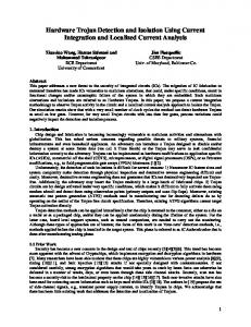
Figure 1. Test CUT. provide adequate resolution to enable the detection of resistive defects. Methods designed to use power supply transient signals for defect detection need to incorporate a mechanism to deal with the signal contribution introduced by defect-free signal propagation. Many test sequences will cause signals to propagate along multiple paths, increasing the difficulty of obtaining reliable detection for cases in which many of the sensitized paths are not affected by the defect. This increases the challenge of devising a general purpose method that is effective under any type of circuit topology and therefore, there are few works on this topic in the literature.
CUT Characteristics CUT Design A block diagram of the CUT investigated in this work is shown in Figure 1. It consists of a 60 by 21 two-dimensional array of test circuits. Each test circuit can be individually activated to provide a test stimulus to the power grid, by itself or in combinations with other test circuits in the array. The power grid is wired in two metal layers as shown in Figure 2. A set of 21 power supply taps, labeled 0 to 20 in Figure 1, emulate the multiple connection points of a typical power grid used in commercial designs. These taps will subsequently be referred to as VDDx where x represents one of the tap connections. In order to emulate probe card contact resistance (Rp), on-chip resistances ranging from 1 Ω to 100 Ω were inserted in series between the
SUBSTRATE
Figure 2. Test CUT’s power grid. .
tap points and each of the power supply C4 pads as shown on the right side of Figure 1. The entire chip is partitioned into “Quads” which are identified as regions surrounded by 4 VDDx tap points, labeled Q0 through Q11 in Figure 1. Each Quad has a total of 121 test circuits (with the exception of Q10 and Q11 which have one less row.) Calibration Circuits Our multiple supply pad testing methodology is very sensitive to probe card contact resistance variations. The contact resistance manifests itself at the interface of the probe card and the CUT C4 solder ball. This contact resistance will not only vary from touch down to touch down but also from one supply pad to another. The contact resistance variations will manifest as anomalies in the measured distribution of the multiple supply pad currents. The presence of defects will also cause regional signal anomalies. Therefore, it is difficult to distinguish between testing environment variation and defects using only the currents measured under the logic tests. To overcome this drawback, we introduced a DFT structure called a ‘Calibration Circuit’ which is described in detail in reference [16]. The basic function of the calibration circuit is to provide stimulus at known locations in the chip. Each CUT calibration cell is activated individually and the corresponding branch current measurements are made at all the supply pads. To compensate for performance variations in the calibration circuit themselves, each of the branch currents are normalized by dividing them by the total current drawn by the CUT. This data is then used in conjunction with the calibration circuit data generated from simulations to calibrate the CUT’s branch currents obtained under the logic tests. The details of the procedure will be discussed in the following section. The test circuits at positions shown by the shaded blocks (the VDD tap points) in Figure 1 are designated as the calibration circuits in this work. The benefit of using the calibration circuit is not limited to just calibration of probe card contact parasitic. It also forms an integral component in the analytical approach of the defect detection procedure discussed in a later section. Calibration Procedure As mentioned earlier, the contact resistances of the probe card will vary not only from touch-down to touch-down but also from pad to pad. The probe card contact resistance varia-
V1 R 1 p
R1
X
Y
R2
Logic Test
C1
Z
Rp2 V2
C2
(a)
V1
Rp
R1
X
Y
R2
C1
Z
Rp
V2
C2
(b) Figure 3. (a) Test Case (b) Simulation Case. tion will distort the natural current distribution determined by the power grid alone. In order to reduce (ideally eliminate) the impact of probe resistance on the current distribution profile, it is necessary to calibrate the measured currents. In this section, we briefly illustrate the basic principles of the calibration procedure using a simple two-port network shown in Figure 3. The circuit in Figure 3(a) represents the test case and the circuit in Figure 3(b) represents the simulation case. The test case has probe resistances Rp1 and Rp2 while the simulation case has a uniform probe resistance of Rp. First the calibration circuit (C1) at location X is turned on in the test case. The currents through V1 (I1CXT) and V2 (I2CXT) are measured1. Similarly, currents I1CZT through V1 and I2CZT through V2 are measured by turning on calibration circuit C2. The same procedure is performed on the simulation model generating currents I1CXS, I2CXS, I1CZS and I2CZS. I1T and I2T represent the currents through V1 and V2 respectively when a defect at location Y is provoked under a logic test in the test case. Using the eight calibration circuit measurements, the currents I1T and I2T can be transformed into currents I1S and I2S that would have been measured if the test case had uniform probe resistances of Rp. I1CXT I 2CXT I1CZT I 2CZT A
⋅
a1 b1 a2 b2 X
=
I1CXS I2CXS I 1CZS I 2CZS
(Eq. 1)
B
In Equation 1, matrix A contains calibration data from the test case, matrix B contains calibration data from the simulation 1.*A note about the subscripts in Ipqrs: p= 1 or 2: voltage source identifier, q=’C’ denotes that it is a calibration test, r=X,Y,Z: location identifier and s= T,S: test case or simulation case identifier.
case and the matrix X contain a set of constants that redistribute the currents measured through the multiple supply pads. This system of equations is solved to obtain the transformation matrix X by computing the inverse of A and multiplying by matrix B. Once the transformation matrix is computed, the test measurements made under a logic test are calibrated using X as shown in Equation 2. Though the expressions shown here are for a 2-VDD port model, the technique can be applied to any n-VDD port model. I 1T I 2T ⋅
a1 b1 a2 b2
=
I I
1S
(Eq. 2)
2S
In the absence of grid variations and grid modelling inaccuracies, the transformation is exact. In our experiment, we created an extracted R-only netlist of the CUT’s power grid and ran SPICE simulations by inserting current sources at the locations indicated as the calibration circuit locations. A uniform probe resistance value (Rp) of 1Ω was chosen for the simulations. Detailed analysis for this choice is presented in [15]. Once the test measurement data is calibrated for probe card contact resistance variations, it becomes possible to implement a reliable defect detection technique discussed in the next section. Hyperbola Method of Defect Detection In this work, we propose a novel defect detection procedure that is based on a geometrical model. The basic strategy underlying the fault detection method is to make use of the spatial variations in the transient signals measured individually at each power supply pads as a means of detecting the presence of a fault. Our previous work [14, 15] suggests that the power supply signal variation introduced by the defect will manifest in the surrounding supply pads proportional to the “equivalent impedance” between the defect site and each of the pads. In order to detect a fault, it is necessary to develop a reliable method of comparison between defect free chips and defective chips that accounts for process variation as well. In previous work, we determined that the magnitude of the steady-state current (IDDQ) drawn by a defect is proportional to the “equivalent resistance” between the defect site and each of the supply pads [4]. The method maps the measured IDDQs to a physical location in the layout. This technique could be extended to IDDT as well. In this case, the area under the IDDT waveform is used for defect detection. However, in this work we analyze average values of the measured IDDT signals for the detection procedure. The mapping procedure translates the measured multiple supply pad currents to an (x,y) layout position that represents the “center of activity” or “centroid”. Under a test sequence that provokes a defect, the supply pad currents are composed of two parts, a portion due to the contribution of the defect and a portion introduced by defect-free signal propagation. The map-
VDD1
Gnd2
Gnd5
VDD3
10000
δ01
Vdd1
λ
Vdd3
10000
δ02
Vdd1
Vdd3
λ Vdd1
10000
11.59
Intersection of horizontal and vertical hyperbolas is predicted location of the “centroid”
11.59 10.98 10.98
8000
8000
8000
10.37
10.37
9.76
9.76
9.15 9.15 8.54
6000
8.54
6000
6000
7.93
7.93
Vdd3
Thu Jun 12 02:43:49 2003
Wed Jun 11 22:42:08 2003 12.20
12.20
7.32
7.32 6.71 6.71
4000
4000
Gnd1
Gnd4
4000
6.10
6.10
5.49
5.49
Lower left quadrant of Quad
4.88 4.88 4.27
2000
2000
4.27
2000
3.66
3.66
3.05
3.05 2.44
(a)
Vertical hyperbola segment
13.4
(b)
14.6
λ
15.9
8.5
9.8
11.0
12.2
13.4
14.6
17.1
x Horizontal hyperbola segment
(c)
λ
15.9
Vdd0
Vdd2
17.1
x
(d)
8000
12.2
7.3
10000
11.0
6.1
6000
9.8
4.9
10000
8.5
3.7
8000
7.3
0
Vdd2 2.4
6000
6.1
1.2
4000
4.9
0.0
0
3.7
Vdd0
0.00
4000
0.61
-1.2
2000
x
2.4
10000
1.2
8000
VDD2
0.0
6000
Gnd3
-1.2
4000
Gnd0
1.22
0.00
2000
VDD0
Vdd2
0
1.83
Vdd0 0
y
0.61
y
1.22
2000
0
1.83
y
2.44
0
λ
Figure 4. Current fraction contours and “centroid” prediction.
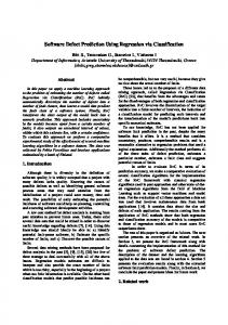
ping procedure for fault detection uses both portions in the analysis and therefore, the (x,y) coordinates returned by the mapping procedure are an abstraction that do not carry any special significance. This is true because the defect-free signal portion of the total current is likely to be generated from signal propagations that are widely distributed in the layout. The magnitude of the IDDT signal introduced by defect-free signal propagation and defects varies widely depending on the test sequence and the nature of the defect, respectively. Ideally, the layout position predicted by the mapping procedures should be independent of the signal magnitudes. To eliminate any dependence on signal magnitude, in this work, we propose current fractions. Here, the current fraction, δxy, defined for a supply pad pair x and y is given by Equation 3.
Ix δ xy = -------------Ix + Iy
(Eq. 3)
In Equation 3, Ix and Iy represents the IDDT signals measured through the supply pads VDDx and VDDy respectively. In this experiment, average IDDT values are used for Ix and Iy. In an earlier work [4], exhaustive set of spice simulations were run by inserting current sources individually at each location on a portion of a commercial power grid as shown in Figure 4(a). The portion of the power grid comprised of four VDD pads and six GND pads. The branch currents measured at each of the four VDD supply pads were used to generate the current fractions as defined in Equation 3. The current fractions for each VDD pair were sorted and contours were plotted as shown in Figure 4(b) and 4(c). Figure 4(b) shows the current fractions generated by VDD0-VDD1 pairing whereas Figure 4(c) illustrates the contours for VDD0-VDD2 pairing. A curve within a contour plot is all the (x,y) layout positions that produce a similar current fraction (within a small tolerance ε) for a given pair of VDDs. The regularity of the contours suggested the existence of an analytical description of these curves. A model based on hyperbola were found to be adequate in describing these contours. For determining the “centroid”, appropriate vertical and horizontal hyperbola curves are chosen based on the measurements made at the different supply
pads and using special structures called “calibration circuits”. The calibration circuits provide the maximum and minimum bounds on the current fractions that are then used to completely define the correct set of vertical and horizontal hyperbolae. The intersection of the vertical and horizontal hyperbolae indicate the location of the “centroid” in the layout as shown in Figure 4(d). Detailed mathematical analysis of the hyperbola fits can be found in [16]. The main idea behind the proposed multiple supply pad detection procedure is that it compares the “centroids” of the CUT with the “centroids” for a defect-free chip for all quads in the chip. If the defect is of significant strength, the “centroid” in at least one quad of the defective chip will be at a different location than the “centroid” for that quad in the defect free chip. To distinguish defective behavior from process variation, multiple defect free chips are analyzed. For all the defect free chips, the “centroids” in every quad will follow a distribution. We assume that the “centroid” predictions in each quad for all the defect free chips obey an elliptical gaussian distribution with independent standard deviations in the x-direction and y-direction. Under this assumption, we create an elliptical region around the cluster of defect free “centroid” predictions in every quad. The dimensions of the ellipse are determined by the 3σ values in the x (3σx) and y (3σy) directions respectively. This 3σ elliptical region around the defect free “centroid” predictions represent a “process variation zone”. The 3σ ellipse becomes a circle if the standard deviations in the two dimensions become equal. If the “centroid” in any quad of the defective chip lie outside the 3σ ellipse for that quad then the defect is claimed to be detected in that quad. The defect must be detected in at least one quad of the chip in order to claim a successful detection. However, the level of confidence of detection increases if the defect is detected in more than one quad of the chip. Hardware Experiments Hardware experiments were conducted on nine copies of a test chip to validate the defect detection procedure described in the previous section. The average of the total IDDT current and the average branch IDDT currents were measured using Keithley 2400 sourcemeters as each of the test circuits on each chip was individually activated. Henceforth we will refer to
2
defect free1 test circuits 0
defect 1 Vdd2
x
5
4
8
7
6
11
10
9
Vdd1
Q1
3
calibration circuits
13
17
16
20
19
defect 1 “centroid”
defect 2 “centroid”
u n d e te c te d d e f e c t a c tiv a te d a t 1 3 , 5 1
Vdd4 detected defect activated at 21, 8 undetected defect activated at 13, 51
12
x
Vdd0
Q0
Vdd5 14
d e te c t e d d e f e c t a c t iv a t e d a t 2 1 , 8
Vdd3 detected defect activated at 21, 8
3σx 3σy
15
defect 2 18
Figure 5. Distribution of 25 defect free test circuits. these average IDDT branch currents as just branch currents. The branch currents were measured using a custom board that allowed automated switching across the 21 VDD ports. The total leakage and branch leakage currents were also measured in each chip. In this case, no test circuits were enabled. The leakage currents were subtracted from the currents measured with the test circuits enabled. The hardware measurements were calibrated using simulation data and hardware calibration circuit measurements. In order to explore the sensitivity of the procedure, we constructed 11 different experiments, each experiment with a different number of test circuits activated to emulate defect free activity. The defect free cases ranged from 1 activated test circuit to 50 activated test circuits. In all the 11 test cases, the locations of the defect free test circuits were chosen randomly. To obtain, maximum flexibility in the experimental design, the test cases were not constructed by activating multiple test circuits simultaneously. Rather, the different experiments were constructed by superposing the branch current contributions of each individual test circuit. For e.g. if we desired to have “n” test circuits activated, then the total current drawn by any supply pad VDDx is given by the sum of all the individual branch currents IVDDx for all the “n” test circuit locations as shown in the Equation 4. The superposed branch currents were normal(Eq. 4) = ΣI vddx total n ized by dividing by the superposition of the total currents of all the “n” test circuits to eliminate dependency on absolute signal magnitudes. I vddx
The above mentioned experimental plan gives maximum flexibility in studying a wide range of test scenarios. A very important concern in using this strategy is that when many test circuits are activated simultaneously, there may be substantial voltage drops in the power grid which would not be accounted for when using the above scheme. Keeping this in mind, we
defect free centroids Q0 undetected defect activated at 13, 51
Figure 6. Centroid based detection in Q0 and Q1 conducted hardware experiments to study the amount of voltage drop in the grid as a function of the number of simultaneously activated test circuits. Our experiments indicated that about 50 test circuits can be simultaneously activated without significant potential drops in the power grid. The upper limit on the number of activated test circuits was decided by this experiment. Figure 6 illustrates the detection algorithm for one of the experiments in which 25 randomly chosen test circuits were activated to emulate defect free activity. The locations of the activated test circuits are indicated by the “boxes with white dots” in Figure 5. A total of nine copies of the test chip were analyzed, eight of which were used as defect-free chips. The ellipses shown in Figure 6 represent the “process variation zones” for this experiment in the indicated quads. The defect free “centroid” predictions are also indicated in Figure 6. Due to space limitations, only two quads (Q0 and Q1) are shown. The ninth chip was treated as the defective chip. In this chip, each test circuit was activated individually to emulate a defect in addition to the ones that were activated for the defect free case. Henceforth we will refer to the test circuits that were used to emulate defects as defects. Figure 6 shows the “centroids” in quads Q0 and Q1 when ‘defect 1’ and ‘defect 2’ (indicated in Figure 5) were activated individually. It is clear from Figure 6 that ‘defect 1’ was detected in quad Q0 but not in quad Q1. ‘Defect 2’ was not detected in any of the two quads shown. Detailed analysis revealed that ‘defect 1’ was detected in four different quads (Q0, Q4, Q10 and Q11). However the maximum residual for ‘defect 1’ was in quad Q0. ‘Defect 2’ was not detected in any of the twelve quads of the test chip. Figure 7 shows a histogram that summarizes the detection results for all eleven experiments. The x-axis in Figure 7 indicates the number of test circuits that were activated for the defect free case and the y-axis represents the number of detections. Though the CUT had 1260 test circuits, 21 of them were used as calibration circuits and the remaining 1239 were used as defects. From Figure 7, we observe that in most of the experiments, our detection technique was able to detect more than
Mean Standardized Residuals
1200
1 20 0
Number of detections
1 00 0
800
80 0
60 0
400
40 0
20 0
0
0
6
6
5
4
4
3
2
2
1
0
0
1 1
5 2
10 15 20 25 30 35 40 45 Number of defect free test circuits Figure 7. Detection results. 3
4
5
6
7
8
9
10
50 11
80% of the defects except for x=40 where only 35% of the defects were detected. A closer look reveals that increasing number of defect free test circuits result in less number of detections. For e.g. the number of detections from x = 1 to 35 are all above 1058, whereas for 40 it is 435, for 45 it is 1023 and for 50 it is 991. This is an expected trend because increasing defect free activity in a chip will overwhelm the effect of the defect thus making it less visible as an anomaly. In other words, the defect would not be able to pull the “centroid” significantly away from the defect free “centroids” as the amount of defect free activity increases in the chip. The number of detections for the case when 40 defect free test circuits were activated is quite lower than the other ones. This is most probably due to the distribution of defect free test circuit locations in the layout. We are currently investigating the dependency of detection sensitivity on the distribution of the defect free test circuit locations and will present the results if this work is accepted. Figure 8 shows the mean standardized residual for each of the 11 experiments indicated on the x-axis. The mean standardized residual gives a notion of the average level of confidence for all the valid detections for each experiment. Contrary to our expectations, no general trend is visible in the mean standardized residuals. The confidence associated with a positive defect detection, expressed in the magnitude of the mean standardized residual, is expected to be smaller for test scenarios in which large numbers of defect free test circuits are activated than the confidence associated with test scenarios with a smaller number of activated defect free test circuits.
Conclusions
In this paper we explored the possibilities of defect detection using average transient power supply signals. We conducted hardware experiments to validate our method. Hardware experiments show that the power grid creates regional behavior that can be used for defect detection purposes. A novel IDDT defect detection technique based on geometry was implemented. Our experiments indicate that even in the presence of heavy defect free activity, the proposed method could detect, in most scenarios, almost 80% of the defects which were scattered throughout the entire layout. Acknowledgements We thank Anne Gattiker, Sani Nassif, Chandler McDowell and Frank Liu at IBM Austin Research Laboratory for their
1 1
5
10 15 20 25 30 35 40 45 Number of defect free test circuits Figure 8. Mean standardized residuals
2
3
4
5
6
7
8
9
10
50 11
support in this project.
References
[1] ITRS (http://public.itrs.net/) [2]A. Germida, Z. Yan, J. F. Plusquellic and F. Muradali, “Defect Detection using Power Supply Transient Signal Analysis”, In proceedings 1999 International Test Conference, 67-76 [3]J. F. Plusquellic, D. M. Chiarulli, and S. P. Levitan. “Identification of Defective CMOS Devices using Correlation and Regression Analysis of Frequency Domain Transient Signal Data,” In proceedings 1997 International Test Conference, 40-49. [4]C. Patel, E. Staroswiecki, S. Pawar, D. Acharyya, and J. Plusquellic, ”Diagnosis using Quiescent Signal Analysis on a Commercial Power Grid”, In proceedings 2002 International Symposium for Testing and Failure Analysis, pp. 713-722 [5]J. F. Frenzel and P. N. Marinos, “Power Supply Current Signature (PSCS) Analysis: A New Approach to System Testing”, In proceedings 1987 International Test Conference, pp. 125–135 [6]S. Su and R. Makki, "Testing Random Access Memory by Monitoring Dynamic Power Supply Current”, Journal of Electronic Testing, Theory and Applications, Vol. 3, No 4, pp. 265-278, 1992. [7]J. S. Beasley, H. Ramamurthy, J. Ramirez-Angulo, and M. DeYong, “IDD Pulse Response Testing of Analog and Digital CMOS Circuits”, In proceedings 1993 International Test Conference, pp. 626–634. [8]M. Sachdev, P. Janssen, and V. Zieren, “Defect Detection with Transient Current Testing and its Potential for Deep-Submicron CMOS ICs”, In proceedings 1998 International Test Conference, pp. 204-213. [9]B. Vinnakota, W. Jiang and D. Sun, “Process-Tolerant Test with Energy Consumption Ratio”, In proceedings 1998 International Test Conference, pp. 1027-1036 [10]K. Muhammad and K. Roy, “Fault Detection and Location using IDD Waveform Analysis”, IEEE Design and Test of Computers, Volume 18, Number 1, pp. 42-49, 2001 [11]I. de Paul, M. Rosales, B. Alorda, J. Segura, C. Hawkins and J. Soden, “Defect Oriented Fault Diagnosis for Semiconductor Memories Using Charge Analysis, Theory and Experiments”, In proceedings 2001 VLSI Test Symposium, pp. 286-291. [12]A. Singh, C. Patel, S. Liao, J. Plusquellic and A. Gattiker, “Detecting Delay Faults using Power Supply Transient Signal Analysis”, In proceedings 2001 International Test Conference, pp. 395-404. [13]A. Singh, J. Plusquellic and A. Gattiker, “Power Supply Transient Signal Analysis Under Real Process and Test Hardware Models”, In proceedings 2002 VLSI Test Symposium, pp. 357-362. [14] D. Acharyya and J. Plusquellic, “Impedance Profile of a Commercial Power Grid and Test System,” ITC 2003, pp. 709-718. [15]D. Acharyya and J Plusquellic, “Hardware Results Demonstrating Defect Localization Using Power Supply Signal Measurements”, Accepted for publication in ISTFA 2004 [16]J Plusquellic, D. Acharyya, D. Phatak and A. Singh, "IDDT-based Fault Detection and Localization", (http://www.csee.umbc.edu/ ~plusquel/pubs/todaes_tsa_detect_locate.pdf).