Speed Test and Speed Binning for DSM Designs
Delay Defect Characteristics and Testing Strategies Kee Sup Kim, Subhasish Mitra, and Paul G. Ryan Intel
these IC defects has been demonstrated. For example, Stanford University’s Murphy and ELF35 experiments (0.7- and 0.35-micron technology, respectively) on logic circuits designed with standard cells showed that the output response for 30% to 35% of defective parts depended on the test pattern application speed. In the Murphy experiment, 3 out of 116 defective parts were not detected when tested at slower than the expected operating speed at normal operating voltage.1 In our experience, the exact number of parts with delay defects has varied with the process and the design, but delay defects have typically represented 1% to 5% of the total defect population observed. That is, 1% to 5% of the units failing a test applied at a golden part’s operating frequency have passed the same tests applied at some lower frequency. Achieving the quality levels required by customers has not been possible without addressing these delay defects in the overall test strategy. Unfortunately, design constraints typically prevent data collection across a full spectrum of frequencies. Most designs have a minimum operating frequency, often determined by the on-chip phase-locked loop circuit. Designs operating at gigahertz speeds might not be operable or testable at frequencies below several hundred megahertz. We generally categorize units failing tests at a design’s minimum operating frequency as speed insensitive. This is somewhat arbitrary, and it may be that some failing parts could have passed an even slower test were one possible. However, if we must draw a line between delay defects and gross defects, the design’s minimum operating frequency is a reasonable choice.
Editor’s note: At-speed testing is undoubtedly critical for designs such as highperformance microprocessors. But how much of a role can structural delay testing play in testing these designs? Are speed problems caused by manufacturing variations or random defects? The authors answer these questions, using their testing experience at Intel. —Kwang-Ting Cheng, University of California, Santa Barbara
A LOGIC NETWORK has a timing failure when it fails to operate correctly at the specified speed but can produce correct outputs at slower or faster speeds. In a synchronous sequential circuit, the cause of a timing failure can be excessive propagation delay through combinational logic connected to a storage element—either a flipflop or a latch. (For ease of presentation in this article, we refer to these storage elements as flip-flops.) If a logic network’s output is not stable by the flip-flop’s setup time, the network violates the long path timing constraint. This is called a setup time violation, the focus of this article. Alternatively, if the propagation delay through combinational logic is too short, circuit outputs can start changing before the flip-flop’s hold time, violating the short path timing constraint. This is called a hold time violation, and it too can cause a timing failure. Several factors influence production delay testing and corresponding DFT techniques: defect sources, design styles, ability to monitor process characteristics, test generation time, available test time, and tester memory. We present an overview of delay defect characteristics and the impact of delay defects on IC quality. We also discuss practical delay-testing strategy in terms of test pattern generation, test application speed, DFT, and test cost.
IC timing failures Delay defects are a critical consideration in designing test strategies to achieve outgoing quality goals for ICs manufactured in high volumes. The significance of
8
0740-7475/03/$17.00 © 2003 IEEE
Speed failures due to process variation Products are designed with specific target frequencies. However, in manufacturing, the maximum oper-
Copublished by the IEEE CS and the IEEE CASS
IEEE Design & Test of Computers
ating frequency (fmax) of individual units varies because of process variation and physical defects. A process variation is a small natural variation in physical parameters from unit to unit. Causes of this variation include differences in materials, equipment, or the die’s location within a reticle or on a Maximum operating frequency, fmax wafer. Process excursions can change the Cumulative process distribution mean (process shift) 0.14 2.3 15.9 50.0 84.1 97.7 99.87 units (%) or broaden the distribution and raise the standard deviation (process spread). Probits −3 −2 −1 0 1 2 3 (sigma) Process controls can keep this variation within set boundaries but cannot entirely eliminate it. Process variation can affect Figure 1. Probability distribution for path delay caused by process an entire die uniformly or localize its variation. effects to a smaller area. Typically, one of the impacts of process variation is a concomitant variation in the fmax of each unit manufactured. roughly 0.14% of the units have an fmax greater than 3 Physical defects during manufacturing can also affect sigma below average. fmax. Most defects are gross defects, which cause errors at Typically, companies choose a product’s operating any speed. However, some physical defects introduce a frequency to meet customer and marketing requiredelay, changing fmax without completely crippling the die. ments, as well as to make an economic tradeoff These defects either drop fmax below the desired fre- between yield loss below the operating frequency and quency (killer delay defects) or simply reduce fmax to a the higher value of a faster design. In manufacturing, value above the desired frequency (downbin delay some units don’t achieve the desired operating fredefects). Systematic delay defects (also called process or quency, and engineers must test the speed of the paths intrinsic defects) have a broad impact on the unit, affect- with the longest delays (also called the critical paths) ing the speed of many paths. A random defect (also under worst-case conditions to screen out these units. called a point or spot defect) occurs in a single location In the example illustrated by Figure 1, there will be more than 1,400 slow units for every million manufactured, and affects the speed of only the path it lands on. In some cases, the precise cutoff between localized even if the operating frequency is set at 3 sigma below process variation and a random physical defect is arbi- average. These 1,400 units alone would exceed the total trary. For example, a spectrum of possible line widths quality requirement for most manufacturers, who often extends from the desired width through process varia- target 500 or fewer total defects per million units tion and resistive open to a fully open gross defect, with shipped (DPM). In addition, it may be necessary to distinguish faster cutoffs defined arbitrarily if at all. It is useful, however, to consider process variation and physical-defect mecha- parts to be sold at a higher operating frequency. This practice is known as speed binning. Such tests can be nisms separately. Process parameters generally don’t have fixed val- extraordinarily difficult to create, and speed path test ues. In actual silicon, they usually follow a probability holes are a commonly reported manufacturing quality distribution. Therefore, the delay for a given path will problem. An alternative approach might be to overdesign the also follow such a distribution. Figure 1 shows an exampart, so that virtually all units will operate at the desired ple distribution. For any design, the fmax of the units manufactured marketing frequency. However, the die size, power, and varies according to a distribution driven by the path packaging costs are generally prohibitive. Also, in most delay variation on the design’s critical paths. Even cases, product designers pass significant design speed among defect-free units, there may be considerable fmax improvements directly to consumers in the form of variation. Figure 1 shows a leading-edge processor’s faster products—the gains are rarely available to ease speed distribution. Following this Gaussian distribution, the testing burden. Generally, test engineers must devise
September–October 2003
9
Speed Test and Speed Binning for DSM Designs
No. of units
or very few parts. This is the signature of random physical defects, which are distributed across many paths and are each tested by a different test pattern.
Speed failures due to random defects
Even when the process parameters of a manufactured part are within an acceptable range, a delay defect caused by random events such as the deposition Fail signature of a foreign particle can appear. If the delay added by a defect exceeds the margin or “slack” of the path it lands on, Figure 2. Number of parts failing each pattern in fmax testing of a 0.18it may cause a timing failure. Unlike micron microprocessor. process variation, a delay defect can appear anywhere on the die and can a solution to effectively screen out products that would turn any path into the critical path dominating a part, depending on how much extra delay the defect introbe slower than the target frequency. duces. The tail of the curve in Figure 2 shows a large number of such random defects. Characteristics of process-variation-induced
speed failure When test patterns are applied to test a part, the clock cycle and the primary output with incorrect logic values can be recorded. This record is the part’s fail signature. In a test called the fmax test, test patterns are applied at increasingly higher clock speeds until the unit fails, and the fail signature for each part is recorded. In a defect-free part, relatively few critical paths dominate the fmax over a range of parametric variations in manufacturing and operating conditions. Test patterns exercise distinct paths on each cycle, and we regard parts sharing a common clock cycle and output pins in their fail signatures as having had their fmax dominated by the same path. When parts fail because of processrelated speed variation, many parts share a very limited number of fail signatures. Figure 2 shows the first-fail data from a microprocessor manufactured in a 0.18-micron process. The x-axis represents the different fail signatures, and the y-axis represents the number of parts having each fail signature in common. In this figure, the fail signatures are ordered along the x-axis by their y value (that is, the x-axis does not represent the test application order). This data shows that a few different fmax fail signatures appear for many units. In general, this is the signature of ordinary process variation, which is usually dominated by few critical paths. The figure also shows that many different fail signatures correspond to the long xaxis tail; each fail signature is associated with only one
10
Measuring size and incidence of delay defects Distinguishing random delay defects from normal process variation during manufacturing is difficult. However, two complementary techniques can differentiate random delay defects from ordinary process variation after a thorough postmanufacturing analysis of the fmax data. The first technique focuses on analyzing the number of units sharing each fail signature. This is the signaturebased approach discussed earlier and illustrated by Figure 2. Its key assumption is that units whose fmax speeds are dominated by the same path will share common fail signatures in an fmax test. In the first step of the analysis, we regard units sharing a fail signature with very few other parts as containing physical delay defects. Unfortunately, this approach cannot distinguish delay defects on critical paths from normal process variation. A second technique completes the analysis. This is the frequency distribution technique, which analyzes the fmax data for all units sharing a common fail signature. Normal process variation results in fmax values with a Gaussian distribution. Outliers to this normal distribution fall outside the envelope of normal process variation and are probably due to random delay defects. As an example of such an analysis, Figure 3 shows a histogram of fmax observations for a single test pattern. In this experiment, the analyzed pattern determined fmax for more than 12,000 units. Four of the observed units
IEEE Design & Test of Computers
No. of units
No. of units
Minimum frequency Operating frequency
Maximum operating frequency, fmax
Maximum operating frequency, fmax
Figure 3. Histogram of fmax observations for a
Figure 4. Distribution of failing frequency for
single test pattern applied to more than 12,000
units with delay defects.
units. Delay defects are outliers to a Gaussian distribution of fmax. VDD
are clear outliers to the normal distribution, exposing delay defects on critical paths tested by this pattern. We needed at least 100 data points to establish a distribution and recognize clear outliers. Figure 4 summarizes the results of another experiment, in which we performed the same analysis on more than 150,000 units of a microprocessor manufactured in a 0.18-micron process. Nearly 1,000 of these units contained a delay defect of some kind. The histogram plots the fmax of each unit determined to contain a delay defect. This part operated in the gigahertz range, with a minimum operating frequency of several hundred megahertz. Interestingly, many of the delay defects occurred in parts that continued to operate above the desired frequency. These defects have no impact on a product sold at a single frequency, but many manufacturers use speed binning to identify faster units to be sold at a higher frequency, and such defects can change the bin a particular unit belongs in. An implication is that any speed-binning strategy must also account for random delay defects. It is also interesting that the frequency required to screen the delay defects varied. This implies that a structural-delay-defect-screening strategy that cannot run at full speed might still play an important role in total defect control by screening a significant, measurable portion of defects.
Potential source of small-delay defects Cell libraries for microprocessors and even highperformance ASICs (for example, network processors) provide elementary logic gates differing mainly in their drive capabilities. The prevailing techniques for increas-
September–October 2003
A
A
Stuck-open fault B
B
Out B
A
Ground
Figure 5. Stuck-open fault affecting a redundant transistor of an extra-drive NOR gate.
ing drive strength are to properly size the transistors and to create parallel drivers. For example, for a NOR gate, creating redundant paths in the pull-up network produces extra drive to reduce delay in the 0-to-1 transition at the NOR gate output. Research has shown that defects with behaviors similar to stuck-open faults are possible in defective ICs.2 The concern is that even if major defects such as stuck-open faults affect redundant transistors, the overall effect might be that the propagation delay of signals along paths passing through the gate may increase by about 10%.3 In Figure 5, for example, a stuck-open fault affects one of the NOR gate’s redundant transistors, adding a little extra delay on the paths passing through the NOR gate. We are still investigating how likely this class of defects is. Any defects or process shifts that increase interconnect resistance or
11
Speed Test and Speed Binning for DSM Designs
crosstalk sensitivity or that decrease supply voltage or clock skew will cause very small delay defects. Clearly, a substantial number of parts have timing failures, caused by both process variation and random delay defects. Left undetected, these failures occur frequently enough to prevent many products from meeting their outgoing quality goals.
Delay-testing techniques Most delay-testing techniques apply Boolean logic values to a part under test and observe its response at some clock frequency. These techniques belong to the category of Boolean delay-defect testing. Some delay defects, especially those resulting from process variation, can be detected through analysis of the response of process monitors—carefully designed special circuit structures that monitor manufacturing-process characteristics. Examples of process monitors include ring oscillators and trees of NAND gates with controlled delays. Process monitors can be designed to be sensitive to variations in interconnect delays or transistor delays. The insertion of process monitors at various locations on the die and the measurement of several process monitor parameters can help in detecting speed problems caused by process variation outside allowable parameters. There are two major questions related to Boolean testing aimed at delay defect detection: ■ ■
What kinds of test patterns should we apply? At what clock frequency should we apply the test patterns and capture the outputs of the logic network under test?
Test patterns for process-variation-induced systematic delay defects One approach to testing for systematic delay defects caused by process variation is to apply functional test patterns, targeted at specific functional blocks, at the primary inputs and observe the tester’s response. The functional test patterns are generally manually written by designers. For delay testing, designers often target timing-critical paths from various functional units in a design and generate test pattern sequences that exercise these critical paths. The quality of a set of functional test patterns is generally measured by its single-stuck-atfault coverage and in some limited circumstances by the coverage of path delay faults along a set of specified critical paths. It is expected that systematic delay problems caused by process variation will affect several paths of the chip (including the critical paths) and will
12
hence be detected by functional test patterns targeted at exercising the critical paths. An advantage of functional testing is that it exercises the part in the way it can be exercised in the system. However, generating functional tests is a manual process and hence is expensive.4 Writing functional tests that target critical-speed paths is very difficult, and targeting thousands of paths would be beyond the means of most projects.
Test patterns for random delay defects In contrast to systematic defects, random delay defects can appear anywhere on a part. Functional tests that exercise a design’s timing-critical paths are useful for detecting random delay defects that happen to fall along the targeted paths, but such tests alone are not sufficient. Additional test patterns covering the entire design are required. One option is to exercise all possible paths in a design, using the path delay fault model. However, even a reasonably sized design contains billions of paths, so this approach is clearly impractical. The industry practice is to use transition-fault testing. The transition-fault model has three major advantages. First, the total number of transition faults in a logic network is comparable to the total number of stuck-at faults in that network. Second, given an irredundant combinational-logic network, it is theoretically possible to generate a transitionfault test set with 100% fault coverage. Third, with minor modifications, existing test pattern generation and simulation tools for stuck-at faults can be used for transition faults, and the fault model doesn’t require timing analysis. We discuss why timing analysis information should not be used for delay testing in the following section. However, the transition-fault model also has significant limitations. It does not consider which path excites a transition fault or propagates the fault effect. If a transition-fault effect propagates from the fault site along a very short path (that is, a path with a lot of timing slack) from input to output, then depending on the amount of extra delay introduced by the defect, the logic value at the output may reach the correct value by the time the logic value is captured in a flip-flop. The defect could have produced incorrect outputs if the transition-fault effect propagated along one or more long paths in the circuit. ATPG often seeks the easiest path to excite and observe faults, which may correspond to paths with very few gates and, depending on the interconnect delay, may be a path with a lot of timing slack. There have been many attempts to overcome this problem.5,6
IEEE Design & Test of Computers
Impact of timing analysis inaccuracies During the design process, designers perform timing verification to find the frequency at which the design should work correctly after manufacture. Static timing analysis is widely used for this purpose. Timing analysis requires information about a design’s logic gate and interconnect delays. For a design using standard cell libraries, the library description provides information about logic gate delays. For custom-designed logic, a thorough circuit simulation provides the logic gate delays. Interconnect delays are either estimated from the interconnect’s dimensions (leading to an estimate of the associated resistance and capacitance), or the resistance and capacitance values are extracted from the design layout with extraction tools. Because a design must operate over a range of voltages and temperatures, and component delays vary with the operating voltage and temperature, timing analysis is usually performed at various temperature and voltage corners. Several physical factors affect timing analysis accuracy. The part’s temperature, clock skew differences, data patterns on neighboring signals that cause crosstalk, power supply voltage drop due to switching activities or dI/dt effects—all affect path speed. For large designs, the center and the edge may exhibit different speeds, which static or even dynamic timing-analysis tools usually don’t model. This problem becomes even more complex when a single reticle contains two or four dies because a different part of the design is on the reticle’s edge in each position. With all these factors, timing values predicted by static timing analysis tools can be grossly inaccurate. This inaccuracy reduces our confidence in any fault model based on the assumption that relatively accurate timing information is available. To be effective, a fault model for delay defects must not be critically dependent on accurate simulation-based timing analysis.
Delay test patterns with scan-based structural test Automatic generation of functional test sequences for detecting single stuck-at faults in sequential logic circuits with no scan DFT (often called sequential test generation) is a complex problem. Automatic generation of functional test sequences for detecting transition faults in sequential circuits with no scan DFT is even more complex. Scan-based DFT facilitates ATPG for transition-fault testing. However, with conventional scan-based DFT, transition-fault test generation and application are more complicated than stuck-at-fault
September–October 2003
testing. In developing a scan-based transition-fault-testing methodology, we must consider several tradeoffs. Using conventional scan DFT restricts the set of test pattern pairs that are applicable to a logic network. There are two approaches to generating a pair of test patterns with scan: ■
■
skewed-load or launch-on-last-shift testing, in which a single shift of the first pattern scanned into the flipflops produces the second pattern; and double-pulse or launch-on-capture testing, in which the first pattern is scanned into the flip-flops, and the system clock is applied to produce the second pattern in the flip-flops, so that the second pattern is the system’s response to the first pattern.
For architectures using multiplexed scan flip-flops with a scan-enable signal, the launch-on-last-shift approach imposes restrictions on the scan-enable signal’s routing: The scan-enable signal must switch from 1 to 0 very quickly because after the second pattern (a shifted version of the first pattern) appears at the flipflop outputs, the tester must capture the circuit’s response in a time equal to the system clock cycle time. One way to meet this requirement is to route the scanenable signal as a clock tree. However, routing another high-speed signal with clocklike accuracy, in addition to the clocks required for system operation, can be expensive. An alternative is to use a pipelined approach for scan-enable signal distribution. In contrast, the launch-on-capture approach imposes no constraint on the routing of the scan-enable signal for multiplexed scan architectures. But it might be impossible to apply some test pattern pairs that can be applied using the launch-on-last-shift approach. However, if detecting a transition fault requires a test pattern pair that the launch-on-capture approach cannot generate, then it is guaranteed that the pattern pair cannot appear in the system flip-flops during normal operation. Although commercial ATPG tools support launch-on-capture transition-fault testing, the execution time and memory requirements are higher than those for launch-on-last-shift testing. With scan-based transition-fault testing, some test pattern pairs applied to detect transition faults might not appear during normal operation because of the circuit’s sequential structure. In that case, paths that cannot be exercised during normal operation, called false paths, can be exercised during test mode. Depending on the design and the speed at which logic values are captured,
13
Speed Test and Speed Binning for DSM Designs
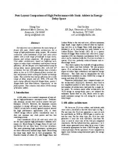
X1
D1 C1
D1
q1
Xm
Y1
Combinational circuit N1 qs Yk
C1
Clk1
Xm +1
D1 C1
D1
q1
Y1
Combinational circuit Y s N2 qk
C1
Z1
Zr
Clk2
Zr +1
Figure 6. Single-latch design with two nonoverlapping clocks.
transitions propagating along false paths might not settle down to the logic value expected from fault-free simulation, which doesn’t account for actual logic gate and interconnect delays. This can cause a defect-free circuit to be declared defective, resulting in yield loss. This issue is distinct from the issue of sequentially redundant stuckat faults detected by scan tests, which we discuss later. The number of transition-fault test patterns in a test set with adequate coverage is significantly higher than that of single-stuck-at-fault test patterns. Compression techniques have become available recently to tackle this problem.7-10
Clock speed for delay defect detection Suppose we have test pattern pair for testing a transition fault. During production testing, we must decide how long to wait after applying v2 before strobing the network’s response into the system flip-flops. Data from a leading-edge microprocessor indicates that the delay between the application of v2 and the capture of the system response must be very close to the clock period. The delay can be 105% of the clock period to account for differences between the tester environment and the actual system without significantly affecting DPM. As explained earlier, false paths can be exercised during scan-based transition-fault testing. Delays along false paths aren’t generally guaranteed to meet the clock cycle time and can be significantly longer. Hence, when the tester captures the logic network’s response after one clock period or very close to that, it is possible that the destination flip-flop will not correctly capture the response of a transition sensitized along a very long false path. This issue is distinct from the issue of sequentially
14
Xn
Zt
redundant stuck-at faults because stuckat-fault testing is usually performed very slowly. Hence, signals propagating along false paths should have enough time to settle down before the logic values at the outputs of the network under test are captured. The launch-on-capture approach to delay testing can minimize but not eliminate this problem because it is difficult during ATPG to determine whether the first pattern scanned into the flip-flops is a valid system state that can appear in the flip-flops during normal operation.
Time borrowing and structural delay testing Another problem related to scanbased delay testing is characteristic of many high-speed designs such as microprocessors, graphics processors, and chipsets. These designs follow the two-phase clock, single-latch design style shown in Figure 6. This design style is used in several Intel products.11 In Figure 6, the clock period of both Clk1 and Clk2 is T. Also, suppose that both Clk1 and Clk2 are square waves with a duty cycle of 1/2. Let us assume an ideal situation in which there are no clock skews. To simplify the discussion, we also assume that Clk1 and Clk2 are nonoverlapping and that Clk2 is an inversion of Clk1. During normal operation, the output of combinational-logic network N2 must be stable at the correct value by time tsetup before the falling edge of Clk1, where tsetup is the setup time of a D latch. Consider the following scenarios: Scenario 1. Suppose that for one of the system’s Clk1 latches, its D input becomes stable at tsetup before the falling edge of Clk1. Thus, the maximum delay through combinational-logic network N1, from tsetup before the falling edge of Clk1 to tsetup before the falling edge of Clk2, can equal T/2. Figure 7a illustrates this scenario. Scenario 2. Suppose that for one of the system’s Clk1 latches, its D input (an output of N2) becomes stable at time ∆ + tsetup before the falling edge of Clk1. Thus, the maximum delay through N1, from ∆ + tsetup before the falling edge of Clk1 to tsetup before the falling edge of Clk2, can equal (T/2) + ∆. This scenario, shown in Figure 7b, is often called time borrowing, as if N1 is borrowing time from N2. If the D input of the Clk1 latch is stable exactly at the rising edge of Clk1, and no hold time violation exists, time borrowing can make the
IEEE Design & Test of Computers
effective delay through N1 equal to T. Suppose that all latches clocked by Clk1 are scanned and a pattern pair is applied. The question is, for effective delay testing, what should the delay be between the application of v2 and the falling edge of Clk2? Following the time-borrowing scenario (scenario 2), the delay must equal (T/2) + ∆max + tsetup, where ∆max is the maximum ∆ in the overall system, which can be as large as almost (T/2) – tsetup. Thus, N1 gets enough time to propagate a transition to its outputs. Otherwise, the captured logic values will be different from expected logic values obtained by fault-free simulation, which pays no attention to logic gate and interconnect delays, resulting in a significant amount of yield loss. In that case, however, for sections of N1 that belong to scenario 1 (that is, the delay through N1 is T/2), a delay defect that causes an extra delay of less than ∆max will be undetectable. Applying multiple Clk1 and Clk2 pairs can generally reduce the severity of this problem. However, such an approach increases the complexity associated with ATPG.
tsetup T/2
Clk1
T/2 tsetup Clk2 N1 delay = T/2 N2 output stable here N1 output must be stable here (a) tsetup T/2
Clk1 ∆
T/2 tsetup
Clk2 N2 output stable here
Effective N1 delay = T/2 + ∆
N1 output must be stable here
(b)
A SIGNIFICANT PORTION of defective parts contain tim-
ing failures caused by process variation and localized random delay defects. In general, one cannot bypass delay defect screening by overdesigning the part. For systematic delay defect detection, relatively few functional or path delay tests targeted toward timing-critical paths and process monitors may be sufficient. For random delay defects, high-quality transition-fault testing is necessary. Structural delay testing requires careful examination to eliminate any cause of potential yield loss or test escape, especially in a certain class of latch-based designs that accommodate time borrowing. Test economics necessitate the adoption of test compression techniques for high-quality delay testing, in addition to stuck-at-fault testing, for multimillion-gate designs. ■
Figure 7. Scan-based delay testing: scenario 1, without time borrowing (a); scenario 2, with time borrowing (b).
2. J.C.M. Li and E.J. McCluskey, “Diagnosis of Sequence Dependent Chips,” Proc. 20th IEEE VLSI Test Symp. (VTS 02), IEEE CS Press, 2002, pp. 187-192. 3. C.-H. Chia et al., “Validation and Test of Network Processors and ASICs,” Proc. 20th IEEE VLSI Test Symp. (VTS 02), IEEE CS Press, 2002, p. 407. 4. A. Carbine and D. Feltham, “Pentium Pro Processor Design for Test and Debug,” Proc. Int’l Test Conf. (ITC 97), IEEE Press, 1997, pp. 294-303. 5. E.S. Park, M.R. Mercer, and T.W. Williams, “Statistical Delay Fault Coverage and Defect Level for Delay
Acknowledgments We gratefully acknowledge Robert Elo and Mike Tripp for their initial work on speed failure data collection and microprocessor design analysis. We also gratefully acknowledge discussions with Mike Lin, David Wu, Sanjay Sengupta, and Derek Feltham of Intel and E.J. McCluskey of Stanford University.
Faults,” Proc. Int’l Test Conf. (ITC 88), IEEE CS Press, 1988, pp. 492-499. 6. C.W. Tseng and E.J. McCluskey, “Multiple-Output Propagation Transition Fault Test,” Proc. Int’l Test Conf. (ITC 01), IEEE Press, 2001, pp. 358-366. 7. B. Koenemann et al., “A SmartBIST Variant with Guaranteed Encoding,” Proc. 10th Asian Test Symp. (ATS 01), IEEE CS Press, 2001, pp. 325-330.
References 1. C.W. Tseng, J. Li, and E.J. McCluskey, “Experimental
8. S. Mitra and K.S. Kim, “X-Compact: An Efficient Response Compaction Technique for Test Cost Reduc-
Results for Slow-Speed Testing,” Proc. 20th IEEE VLSI
tion,” Proc. Int’l Test Conf. (ITC 02), IEEE Press, 2002,
Test Symp. (VTS 02), IEEE CS Press, 2002, pp. 37-42.
pp. 311-320.
September–October 2003
15
Speed Test and Speed Binning for DSM Designs
9. S. Mitra and K.S. Kim, XPAND: Deterministic Test Generation with Very Few Scan Pins and Lots of Scan Chains, tech. report, Intel, 2003. 10. J. Rajski et al., “Embedded Deterministic Test for Low Cost Manufacturing Test,” Proc. Int’l Test Conf. (ITC 02), IEEE Press, 2002, pp. 301-310.
Subhasish Mitra is a senior staff engineer at Intel, where he is responsible for design for testability, reliability, manufacturability, and debug (DFX). Mitra has a PhD in electrical engineering from Stanford University.
11. R. Colwell and R. Steck, “A 0.6µm BiCMOS Processor with Dynamic Execution,” Proc. Int’l Solid-State Circuits Conf. (ISSCC 95), IEEE Press, 1995, pp. 176-177, 381.
Kee Sup Kim is the director of DFX (design for testability, reliability, manufacturability, and debug) in the Intel Communications Group. His research interests include the DFX areas, especially structural test, speed defect coverage, BIST, and quality risk assessment. Kim has a BSEE from the University of Texas at Austin, an MS in electrical engineering from the University of Virginia, and a PhD in electrical engineering from the University of Wisconsin-Madison.
Paul G. Ryan manages Intel’s Product Development Technology Group for Architecture Quality and Reliability. His research interests include tools and technology for reliability, test, and diagnosis, as well as CAD tools and predictive models. Ryan has a BS in electrical engineering from Pennsylvania State University and an MS and a PhD, both in electrical and computer engineering, from the University of Illinois. Direct questions and comments about this article to Kee Sup Kim, Intel Corp., 2200 Mission College Blvd., Santa Clara, CA 95052;
[email protected].
Call for Papers September-October 2004 IEEE Design & Test Special Issue on Embedded Systems for Real-Time Multimedia Guest Editors: Radu Marculescu (Carnegie Mellon University) and Petru Eles (Linkoping University) The design and optimization of modern multimedia systems must address potential hardware-software tradeoffs and their effect on media quality. Most notably, the transition from desktop multimedia to portable multimedia brings concurrency, communication, and time considerations into the driver’s seat for modeling, analysis, and optimization of these systems. Because of the increasing importance of embedded systems for multimedia applications, IEEE Design & Test will publish a special issue in this area. Suggested topics include ■ ■ ■ ■ ■ ■
Specification and design of embedded multimedia systems; Low-power design methodologies and design experiences; Validation and verification; Embedded multimedia architectures; Multimedia processors and reconfigurable architectures; Software optimization and compiler techniques;
16
■ ■ ■ ■ ■ ■
Emerging trends (SoCs, networks on chips) in implementing multimedia systems; Timing aspects of media streams; Scheduling of media processing; Resource and QoS management methods; Temporal estimation and protection of media streams; and Real-time kernels, operating-system, and middleware support.
To submit a manuscript, please access the IEEE Computer Society Web-based system, Manuscript Central, and select “Special Issue on Embedded Systems for Real-Time Multimedia.” In addition, please send a 150-word abstract and the title of your manuscript to Guest Editor Radu Marculescu (
[email protected]). If you wish to be a reviewer, please contact
[email protected]. The deadline for submission is 15 December 2003; see the full call and author guidelines at http://computer.org/dt/.
IEEE Design & Test of Computers