A parallel prefix adder involves the execution of the operation in parallel ... The binary addition is the basic arithmetic operation in digital circuits and it became.
ISSN (Online) 2321 – 2004 ISSN (Print) 2321 – 5526
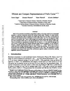
INTERNATIONAL JOURNAL OF INNOVATIVE RESEARCH IN ELECTRICAL, ELECTRONICS, INSTRUMENTATION AND CONTROL ENGINEERING And
National Conference on Advanced Innovation in Engineering and Technology (NCAIET-2015) Alva’s Institute of Engineering and Technology, Moodbidri Vol. 3,Special Issue 1,April 2015
Design and Implementation of different types of efficient parallel prefix adders Mr. Deepak Raj1, Mrs.Sahana K Adyanthaya2 , Prof. Praveen J3, Prof. Raghavengra Rao R4 M. Tech 2nd year, VLSI Design and Embedded Systems, Dept. of ECE, AIET, Mijar, Moodbidri, Karnataka, India 1 Assistant Professor, Dept of ECE, AIET Mijar, Moodbidri, Karnataka, India2 Sr. Associate Professor, Dept of ECE, AIET Mijar, Moodbidri, Karnataka, India3, 4 Abstract: In Very Large Scale Integration (VLSI) designs, Parallel prefix adders (PPA) have the better delay performance. A parallel prefix adder involves the execution of the operation in parallel which can be obtained by segmentation into smaller pieces. The binary addition is the basic arithmetic operation in digital circuits and it became essential in most of the digital systems including Arithmetic and Logic Unit (ALU), microprocessors and Digital Signal Processing (DSP). At present, the research continues on increasing the adder’s delay performance.In this paper the investigation of four types of PPA’s (Kogge Stone Adder (KSA), Spanning Tree Adder (STA), Brent Kung Adder (BKA) and Sparse Kogge Stone Adder (SKA)) is done. Additionally Ripple Carry Adder (RCA), Carry Lookahead Adder (CLA) and Carry Skip Adder (CSA) are also investigated. These adders are implemented in verilog Hardware Description Language (HDL) using Xilinx Integrated Software Environment (ISE) 13.4 Design Suite. The area, delay and power consumed by all types of PPA’s are analyzed. The area of the adder design are given in terms of Look Up Tables (LUT’s) and Input Output bounds (IOB’s). The adder designs are implemented and delay, power and area of all the adders are investigated. Keywords: PPA, RCA, CLA, SKA, KSA, BKA, STAFPGA, Delay, Power, Area I. INTRODUCTION Binary adders are one of the most basic and widely used arithmetic operations in modern integrated circuits. They tend to play a critical role in determining the performance of the design. Arithmetic operations are the regular common operations in digital integrated circuits. The simplest circuit adds, subtracts, and multiplies or divides. The computation should be fast and the area consumed by the arithmetic units should be small. These are the two basic requirements for any adder [2]. Parallel computing isform of computation in which many calculations are carried out simultaneously, operating on the principle that large problems can often be divided into smaller ones, which are then solved concurrently in parallel. There are several different forms of parallel computing: bit-level, instruction level, data, and task parallelism. Parallelism has been employed for many years, mainly in high-performance computing, but interest in it has grown lately due to the physical constraints preventing frequency scaling. As power consumption and consequently heat generation by computers has become a major concern in recent years,parallel computing has become the dominant paradigm in computer architecture, mainly in the form of multi-core processors. Parallel computers can be roughly classified according to the level at which the hardware supports parallelism, with core and multi-processor computers having multiple processing elements within a single machine. Area and Time consumed by the circuit are the basic and important Copyright to IJIREEICE
requirements. Numbers can be represented in digital circuits in various ways. Hence, developing efficient adder architecture is crucial to improving the efficiency of the design. Generally ripple carry adder is used for binary addition. After the design of ripple carry adder several techniques are used for the computation of parallel adders. Carry look ahead adders are based on parallel prefix computation which gives better performance than ripple carry adder. After many years of research, focus is on improving the delay performance of the adder. As such, extensive research continues to be focused on improving the delay performance of the adder. Next, Brent and Kung (BK) designed parallel prefix-computation graph in anarea-optimal way and the kogge-stone (KS) architecture is optimized for timing. The binary addition is the basic arithmetic operation in digital circuits and it became essential in most of the digital systems including Arithmetic and Logic Unit (ALU), microprocessors and Digital Signal Processing (DSP). At present, the research continues on increasing the adder’s delay performance. In many practical applications like mobile and telecommunications, the Speed and power performance improvement in FPGAs is better than microprocessor and DSP’s based solutions. Additionally, power is also an important aspect in growing trend of mobile electronics, which makes large-scale use of DSP functions. Because of the Programmability, structure of configurable logic blocks (CLB) and programming
DOI 10.17148/IJIREEICE
172
ISSN (Online) 2321 – 2004 ISSN (Print) 2321 – 5526
INTERNATIONAL JOURNAL OF INNOVATIVE RESEARCH IN ELECTRICAL, ELECTRONICS, INSTRUMENTATION AND CONTROL ENGINEERING And
National Conference on Advanced Innovation in Engineering and Technology (NCAIET-2015) Alva’s Institute of Engineering and Technology, Moodbidri Vol. 3,Special Issue 1,April 2015
interconnects in FPGAs, Parallel prefix adders have better within the circuit which in turn will have high power performance [1]. consumption. The delay of the 64-bit KSA is 48.064ns and of the Ling adder is 51.841ns. They concluded that several architectures are often close to the optimum performance II. LITERATURE REVIEW Sudheer Kumar Yezerla et al.[1] did research on, “Design for the given design environment. and Estimation of delay, power and area for Parallel Prefix Adders”, where the design was implemented using Xilinx The result obtained shows that the given methodologies Virtex 5 FPGA and the adder delays were estimated using lead to the best design at all technological nodes. Neil Agilent 1692A Logic Analyzer. The 16-bit SKA computes Burgess [5]in the paper, “Fast Ripple-Carry Adders in the carries with Black Cells (BC’s) and Grey Cells (GC’s) Standard-Cell CMOS VLSI”, presented new high-radix ripple carry adder based on Ling’s addition technique. The and terminates with a 4-bit RCA. critical path introduced inverting CMOS cell per stage The 16-bit STA used also terminates with RCA and uses along carry in and carry out. The fastest of them matches BC’s and GC’s and Full Adders but has difference in the speed of 16-bit prefix adder for only 63% of the area. interconnection between them. The 16-bit KSA designed Mangesh B Kondalkar et al. [6] work on, “Improved Fault used 16 BC’s and 15 GC’s with less delay compared to Tolerant Sparse KOGGE Stone ADDER”, proposed a SKA and STA. The 16-bit BKA used 14 BC’s and 11 method for error correction due to inherent redundancy in GC’s which is less compared to KSA and hence has less the carry tree and also error detection was possible. The architecture and occupies less space than KSA. The delay prior work had only error correction which used Kogge measurements show that SKA and BKA have almost same Stone configuration. Several enhancements are introduced delay where as STA has better delay results. The in the design; the error recovery time is reduced by using a efficiency has increased for delay up to 5.77% for RCA 16-bit register, error correction due to fault in multiple and for KSA has improved by 19.28%. ripple carry adders is included which improves the reliability of the circuit. CH. Chimpiraiah et al.[2] work on, “An efficient architecture for Parallel Adders” presents an efficient Triple Mode redundancy Ripple carry (TMR-RC) is structure for parallel adders with fast performance which simple and effective method of fault detection and are particularly attractive for VLSI implementations. The correction but it increases the area overhead and almost simulation and synthesis was done in Xilinx ISE results in tripling of the associated power dissipation. A Foundation 9.2i software. Sparse Kogge-Stone adder which is fully fault tolerant in its lower half (i.e., in the ripple carry adders) was The proposed design was the combination of KSA and proposed. BKA and the result is compared with KSA. The area given in terms of slices was reduced from 81 to 63 and the delay The addition of register reduces the error recovery time from 12.27ns to 11.04ns. The number of logic levels was and also makes it possible to detect and correct the error in reduced from 8 to 7 compared to KSA which gives better multiple RCA. power performance. V. Krishna Kumari et al. [3] III. IMPLEMENTATION OF PARALLEL researched on, “Designing and Characterization of Kogge PREFIX ADDER STRUCTURE Stone, Sparse Kogge stone, Spanning tree and Parallel Prefix Adder Structure BrentkungAdders”,and the results were obtained using 3.1. modelsim 6.4b,Xilinx ISE 10.1i for simulation and Parallel-prefix structures are found to be common in high performance adders because the delay is logarithmically synthesis. proportional to the adder width.PPA’s basically consists of The practical issues while testing the adders were analyzed 3 stages and a circuit to test the adders is designed. The objective Pre computation of the testing adder circuit was to find the worst path and Prefix stage the input causing it was combination which is stored in Final computation ROM. The Parallel Prefix adder structure is shown in Fig 3.1. A.N. Jayanthi et al. [4] work on, “Comparison of performance of high speed VLSI adders” ,proposed 16-bit and 64-bit adder design for all the adders and the comparison was made in terms of delay.
3.2 Implementation stages of PPA PPA’s basically consists of 3 stages: Pre-Computation Stage In pre computation stage, propagates and generates are computed for the given inputs using the given equations The 16-bit Ling adder design proposed has delay reduced (1) and (2). to half compared to the 16-bit RCA, but the circuit has limitations on fan-in. The KSA adder scheme reduces Pi=Ai^Bi (1) logical fan-out in each node but increases the wiring Gi=Ai.Bi (2) Copyright to IJIREEICE
DOI 10.17148/IJIREEICE
173
ISSN (Online) 2321 – 2004 ISSN (Print) 2321 – 5526
INTERNATIONAL JOURNAL OF INNOVATIVE RESEARCH IN ELECTRICAL, ELECTRONICS, INSTRUMENTATION AND CONTROL ENGINEERING And
National Conference on Advanced Innovation in Engineering and Technology (NCAIET-2015) Alva’s Institute of Engineering and Technology, Moodbidri Vol. 3,Special Issue 1,April 2015
The generate/propagate signals can be grouped in different fashion to get the same correct carries. Based on different ways of grouping the generate/propagate signals, different prefix architectures can be created. S i = P i .G i-1:-1 (7) Cout = G n:-1 (8)
4.1
IV. DIFFERENT TYPES OF PPA’S 16-Bit Kogge Stone Adder
Fig 3.1: Parallel-Prefix structure with carry save notation[1]. Prefix Stage In the prefix stage, group generate/propagate signals are computed at each bit using the given equations. The black cell generates the ordered pair and the grey cell generates only the left signal. The fundamental carry operator is denoted by the symbol “o”. The generate and propagate signals are combined using the fundamental operator as shown in equation (3). ( g L, p L ) o ( g R , p R ) = ( g L + pL. gR , pL. gr ) (3) The black cell and grey cell logic definition are shown in Fig 3.2.
Fig 4.1 16-bit Kogge-Stone Adder[1] Kogge-Stone adder is one among the parallel prefix adders. This has regular layout which makes them favored adder in electronic technology. It has the minimum fanout. A 16 bit Kogge stone adder is shown in the figure 4.1. The maximum fan-out is 2 in all the logic levels for all width Kogge-stone prefix trees. The key of building any prefix tree is to implement the structureaccording to the Fig 3.2: Black and Grey Cell logic definition. grey cell and black cell logic. The number of stages for a From the black and grey cell logic definition, the generate Kogge stone adder is calculated by log2 power N. no of cells is calculated as N (log2 power N – 1) +1.It consists and propagate signals are given by equations (4) and (5). of 34 BC’s and 15 GC’s. G i:k = G i:j + P i:j .Gj-1:k P i:k= P i:j . Pj-1:k
(4) (5) 4.2 16-bit Sparse Kogge-Stone Adder The Sparse Kogge stone adder consists of several small More practically, the equations (4) and (5) can be ripple carry adders on its lower part, a carry tree is on its expressed using a symbol “o” denoted by Brent and Kung. upper part. It terminates with ripple carry adders. Number Its function is exactly the same as that of a black cell and of carries generated is less in this adder compared to is given in (6). The “o” operation will help make the rules Kogge stone adder. of building prefix structures [7].
The function of grey cells and black cells is same as G i:k : P i:k =( G i:j , P i:j )o( Gj-1:k , Pj-1:k ) (6) discussed in previous sections. Figure 4.2 shows the block diagram of 16 bit Sparse Kogge Stone adder. Like the sparse Kogge-Stone adder, this design terminates with a 4Final Computation In the final computation, the sum and carryout are the final bit RCA. As the FPGA uses a fast carry-chain for the output. These are given by equations (7) and (8), where “- RCA, it is interesting to compare the Performance of this adder with the sparse Kogge-Stone and regular Kogge1” is the position of carry-input. Stone adders. Copyright to IJIREEICE
DOI 10.17148/IJIREEICE
174
ISSN (Online) 2321 – 2004 ISSN (Print) 2321 – 5526
INTERNATIONAL JOURNAL OF INNOVATIVE RESEARCH IN ELECTRICAL, ELECTRONICS, INSTRUMENTATION AND CONTROL ENGINEERING And
National Conference on Advanced Innovation in Engineering and Technology (NCAIET-2015) Alva’s Institute of Engineering and Technology, Moodbidri Vol. 3,Special Issue 1,April 2015
4.4
16-bit Brent Kung Adder
Fig 4.2 16-bit Sparse Kogge-Stone Adder[1] 4.3 16-bit Spanning Tree Adder Another carry-tree adder known as the spanning tree carry-lookahead (CLA) adder shown in Fig 4.3 is also examined .Like the sparse Kogge-Stone adder, this design terminates with a 4- bit RCA. As the FPGA uses a fast carry-chain for the RCA, it is interesting to compare the performance of this adder with the sparse Kogge-Stone and regular Kogge-Stone adders. Also of interest for the spanning-tree CLA is its testability features. It also uses the black cells and gray cells and full adder blocks like sparse kogge-stone adders but the difference is the interconnection between them.
Fig 4.4 16-bit Brent Kung Adder[1] Another carry tree known as BKA which also uses BC’s and GC’s but less than the KSA. So it takes less area to implement than KSA. The 16 bit BKA uses 14 BC’s and 11 GC’s but kogge stone uses 36 BC’s and 15 GC’s. So BKA has less architecture and occupies less area than KSA. The 16 bit BKA is shown in the below figure 4.4. BKA occupies less area than the other 3 adders called SKA, KSA, STA. This adder uses limited number of propagate and generate cells than the other 3 adders. It takes less area to implement than the KSA and has less wiring congestion. The operation of the 16 bit Brent Kung adder is given below [8]. This adder uses less BC’s and GC’s than Kogge-Stone adder and has the better delay performance. V. RESULTS The simulation results are carried out in ModelSim6.3f design suite and is shown in the fig 5.1.
Fig 5.1: Simulation result of adder
Fig 4.3 16-bit Spanning Tree Adder[1] Copyright to IJIREEICE
The device utilization summary report from Xilinx 13.2 gives the area occupied by each of the adders in terms of slices and LUT’s when used in SPARTAN 3 Field Programmable Gate Array. For 16-bit adder the number of slices occupied is shown in the Table 5.1. The delay for the maximum path in adder design is summarized in Table 5.2. DOI 10.17148/IJIREEICE
175
ISSN (Online) 2321 – 2004 ISSN (Print) 2321 – 5526
INTERNATIONAL JOURNAL OF INNOVATIVE RESEARCH IN ELECTRICAL, ELECTRONICS, INSTRUMENTATION AND CONTROL ENGINEERING And
National Conference on Advanced Innovation in Engineering and Technology (NCAIET-2015) Alva’s Institute of Engineering and Technology, Moodbidri Vol. 3,Special Issue 1,April 2015
[5]. Neil Burgess, ARM Inc ,“Fast Ripple-Carry Adders in StandardCell CMOS VLSI”, 2011 20th IEEE Symposium on Computer Arithmetic, 1063-6889, © 2011 IEEE. [6]. Mangesh B Kondalkar, Arunkumar P Chavan, P Narashimaraja, “Improved Fault Tolerant Sparse KOGGE Stone ADDER”,International Journal of Computer Applications (0975 – 8887) Volume 75– No.10, August 2013. [7]. Niel H EWeste, David Money Harries, “CMOS VLSI DESIGN – A CIRCUITS AND SYSTEMS PERSPECTIVE”, fourth edition. [8]. R. P. Brent and H. T. Kung, “A regular layout for parallel adders,” IEEE Trans. Comput., vol. C-31, pp. 260-264, 1982.
Design Utilization Summary(SPARTAN 3) No. of 4 No. of No. of Adder input bounded Slices LUT’s IOB’s RCA 18 31 49 CKA 21 37 50 CLA 18 32 50 KSA 41 72 50 BKA 21 38 50 Table 5.1: Device Utilization Summary of various adders Xilinx 13.2 ISE tool Adder Delay(ns) RCA 27.34 CSA 33.98 CLA 28.741 KSA 18.588 BKA 23.854 Table 5.2: Delays for various adders VI. CONCLUSION AND FUTURE WORK It is shown that the results obtained for Parallel Prefix Adders are better than the serial adders in terms of delay and at the same time there is a trade-off with the area occupied. The results obtained for carry chain adders at higher bit widths (128 to 256 bits) has higher performance when compared to serial adders. Because the adder is often the critical element which determines to a large part the cycle time and power dissipation for many digital signal processing and cryptographically implementations, it would be worthwhile for future FPGA designs to include an optimized carry path to enable tree based adder designs to be optimized for place and routing. Inclusion of a ROM is being done in few adder designs to find the worst case delay combination of the input. Architectures that include fast carry chains and the possible tradeoffs are investigated. In the future, designs for Spanning Tree Adder(STA) and Sparse Kogge Stone Adder (SKA) are done and delay and area occupied are calculated to check performance enhancement keeping serial adders as reference. REFERENCES [1]. Sudheer Kumar Yezerla, B Rajendra, “Design and Estimation of delay, power and area for Parallel prefix adders”, Proceedings of 2014 RAECS UIET Panjab University Chandigarh, 06 - 08 March, 2014, 978-1-4799-2291-8 ©2014 IEEE. [2]. CH. Chimpiraiah, E.V Vijay, “AN EFFICIENT ARCHITECTURE FOR PARALLEL ADDERS”, International Journal of VLSI and Embedded Systems-IJVES, Vol 03, Issue 04; September-October 2012 ,ISSN: 2249 – 6556. [3]. V.KrishnaKumari, Y.SriChakrapani, “Designing and Characterization of koggestone, Sparse Kogge stone, Spanning tree and Brentkung Adders”, International Journal of Modern Engineering Research (IJMER) , Vol. 3, Issue. 4, July-august. 2013 pp-2266-2270 ISSN: 2249-6645. [4]. A.N. Jayanthi, Dr.C S Ravichandran ,“Comparison Of Performance Of High Speed VLSI Adders”, International Conference on Current Trends in Engineering and Technology, IEEE – 32107 July 3, 2013© IEEE 2013.
Copyright to IJIREEICE
DOI 10.17148/IJIREEICE
176