Energy Efficient Design and Implementation of ALU on 40nm FPGA Bishwajeet Pandey, Jyotsana Yadav, Yogesh Kumar Singh, Rohit Kumar, Sourabh Patel Department of Information Technology ABV-Indian Institute of Information Technology and Management (ABV-IIITM), Gwalior, Madhya Pradesh, India Email:
[email protected],
[email protected],
[email protected], Abstract— There is 67.04% dynamic power reduction with
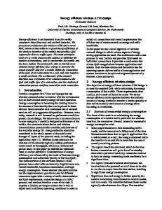
Shift Left A
LVCMOS12 when we migrate from 90-nm Spartan-3 FPGA to 40-nm Virtex-6 FPGA. There is 81.19%, 92.05% dynamic power reduction when using LVCMOS12 in place of HSTL_II_18 and SSTL2_I_DCI respectively. We achieved 65.56%, 72.59% and 73.41% dynamic power reduction in ALU with LVDCI IO standard in place of LVDCI_DV2, HSTL_I, and LVCMOS12 respectively. There is 68.34% and 52.51% dynamic power reduction in ALU when using LVCMOS12 and LVCMOS15 in place of LVCMOS25. There is 62.45% dynamic power reduction in ALU, when we use HSTL_I in place of SSTL2_I_DCI. Power
All Flags are unaffected with Unary Function except Carry for Shift.
is directly proportional to frequency. With increase in frequency, there is increase in power consumption irrespective of IO standard. LVCMOS is the only IO standard, which takes less power when we upgrade our design to latest FPGA. Keywords—FPGA, Low Power, Native Generic Circuit, Dynamic Power, Clock Power, Arithmetic Function, Logical Function, Operation Code, Power Estimation, Behaviour Simulation
I.
INTRODUCTION
Arithmetic Logic Unit is an integral part of any processor design. It performs arithmetic, Logic and Unary function on value stored in accumulator, register array, operand register and fetched value from external memory. In an 8-bit processor, if we mask last four bit of operation code to perform arithmetic and logic operations. With 4-bit we can support a maximum of 16 operations as listed in Table.1. We are taking first eight as unary operation and rest as arithmetic and logic operations. Table 1: Function of Arithmetic and Logic Unit Design Functions of Arithmetic and Logic Unit Unary
Sel
Arithmetic & Logic
Sel
Clear
0000
Add
1000
Hold B
0001
Subtract
1001
Complement B
0010
Add Carry
1010
Hold A
0011
Subtract Borrow
1011
Complement A
0100
Logical AND
1100
Decrement A
0101
Logical OR
1101
Increment A
0110
Logical XOR
1110
0111
Logical XNOR
1111
All Flag set in every operation from 1000-1111.
This ALU takes 2 inputs: A, B. A is 8-bit value fetch from external memory and B is 8-bit value from operand register. Sel is first four bits of 8-bit operation code of processor. Flags are:
Zero
Carry
Sign
Parity
Zero flag is set when all bit of output of ALU is zero. Carry flag is set when result is overflow, underflow and shift either left or right or circular. Sign flag is set to 1 for output in negative (-ve) magnitude and 0 for output in positive (+ve) magnitude. Parity is set to 1 if number of occurrence of 1 in output is even otherwise 0. II.
RELATED WORKS
High speed Look up Table (LUT) is implementing with circuit technique in [1]. In [1] proper sizing of each and every sleep transistors done in the LUT to achieve an optimum power and energy delay relationship so that it can be used for energy efficient applications. Also, [1] implemented a benchmark circuit (8 × 10) encoder in Virtex-4, 90nm FPGA. Now, latest FPGA like Virtex-7 is based on 28-nm technology, so there is need to search other technique to design low power devices. [6] Performs 16 instructions and has a two-stage pipelined architecture and for energy efficiency, a new ALU architecture in [6] has an efficient ELM adder of propagation (P) and generation (G) block scheme. The arithmetic operations of the proposed ALU are disabled when logical operation is going on and vice versa. Double edge-triggered flip-flops are used as basic building block of register [6] to reduce the switching activity for the register. Rest [2-5] describes different FPGA based low power design on different nm technology. Reference [9], uses Clock Gating and turn off the 15 functional units out of total 16 functional units. Hence reduce 93.75% power reduction. In [7], we achieve 35.9% dynamic power reduction and 36.11% dynamic current reduction by shifting drive strength from 24mA to 2mA on LVCMOS25 when 2.5 V is output driver supply voltage and 1.0V is input supply voltage. Techniques in [9] also achieved 30% dynamic power reduction and 21.7%
dynamic current reduction by shfting drive strength from 24mA to 2mA on LVCMOS12 when 1.2V is output driver supply voltage and 1.0V is input supply voltage. III.
LOW POWER ANALYSIS
A. Why Low Power? Increasing sky rocket power budget and socio-economic pressure for green earth is main driver to shift our focus to low power design or energy efficient design. Environmental concern of power production by traditional sources motivate hardware designer for green computing. Either low power or energy-efficiency or green computing is an effort to reduce power consumption and dissipation. The root of all effort is to search power efficient device and energy efficient standard. B. Pre-Synthesis Power Estimation Using Virtex-6 Default operating condition and UCF timing constraint of 1000.0 MHz on clock net 'CLK' in power estimation, RTL dynamic power estimation is 41mw. Total power estimation on alucode is: 1044 mW as shown in Figure.1.
There is 11.11 % dynamic power reduction in ALU when using HSTL class I in place of HSTL class II. There is 81.19% dynamic power reduction when using LVCMOS12 in place of HSTL_II_18. c) Stub Series Transistor Logic SSTL class I (SSTL2_I), SSTL class I with DCI (SSTL2_I_DCI), SSTL class II (SSTL2_II) and SSTL_18_I are different IO standards in SSTL family. The variation in power consumption is dependent on the variance in SSTL class as shown in Table.4. Table 4: Power Consumption with SSTL and 40-nm FPGA 1GHz 1THz
SSTL2_I
SSTL2_I_DCI
SSTL2_II
SSTL18_I
465mW 87.649W
1108mW 131.883W
542mW 172.043W
421mW 60.134W
There is 62.45% dynamic power reduction in ALU, when we use HSTL_I in place of SSTL2_I_DCI. There is 92.05% power reduction in ALU, when we use LVCMOS12 in place of SSTL2_I_DCI. d) Low Voltage Digitally Control Impedance LVDCI_15, LVDCI_18, LVDCI_25 and LVDCI_DV2_25 are different IO standards in low voltage digitally controlled impedance family. The variation in power consumption is dependent on the variance in LVDCI voltage level as shown in Table.5. Table 5: Power Consumption with LVDCI and 40-nm FPGA 1GHz 1THz
Figure 1: Pre-Synthesis & Pre-Implementation Power Consumption
C. Use of Power Efficient IO Standard In order to search power efficient IO standard, we are taking following four families under consideration. These are: a) Low Voltage Complementary MOS LVCMOS12, LVCMOS15, LVCMOS18 and LVCMOS25 are different variety of LVCMOS depending on their output driver supply voltage. The variation in power consumption is dependent on the variance in Vcco as shown in Table.2. Table 2: Power Consumption with LVCMOS and 40-nm FPGA 1GHz 1THz
LVCMOS12
LVCMOS15
LVCMOS18
LVCMOS25
88mW 87.649W
132mW 131.883W
172mW 172.043W
278mW 278.017W
There is 68.34% reduction in ALU when using LVCMOS12 in place of LVCMOS25. There is 52.51% reduction in ALU power consumption when using LVCMOS15 in place of LVCMOS25. b) High Speed Transceiver Logic HSTL class I (HSTL_I), HSTL class II (HSTL_II), HSTL_II_18 and HSTL_I_18 are different IO standards in HSTL family. The variation in power consumption is dependent on the variance in class as shown in Table.3. Table 3: Power Consumption with HSTL and 40-nm FPGA 1GHz 1THz
HSTL_I
HSTL_II
HSTL_II_18
HSTL_I_18
416mW 87.649W
427mW 131.883W
468mW 172.043W
447mW 278.017W
LVDCI_15
LVDCI_18
LVDCI_25
LVDCI_DV2_25
114mW 87.649W
152mW 131.883W
241mW 172.043W
331mW 278.017W
There is 65.56%, 72.59% and 73.41% dynamic power reduction in ALU when we use LVDCI in place of LVDCI_DV2, HSTL_I, and LVCMOS12 respectively. D. Frequency in Reduction LVCMOS12 is taking 88mW power on 1GHz operating frequency. When we increase frequency by 1000 times, then overall power consumption increases but not exactly 1000 times. In this case, there is 998.99 times increase in power consumption with 1000 times increase in frequency. E. Use of Power Efficient FPGA We are taking two FPGA. One is 40-nm Virtex-6 and others are 90-nm Spartan-3. a) Low Voltage Complementary MOS There are four types of LVCMOS. LVCMOS12, LVCMOS15, LVCMOS18 and LVCMOS25 are different variety of LVCMOS depending on their output driver supply voltage. The variation in power consumption is dependent on the variance in Vcco as shown in Table.6. Table 6: 90-nm FPGA versus 40-nm FPGA 40nm 90.nm
1GHz 1GHz
LVCMOS12
LVCMOS15
LVCMOS18
LVCMOS25
88mW 147mW
132mW 148mW
172mW 149mW
278mW 151mW
There is 67.04% power reduction with LVCMOS12 when we migrate from 90-nm Spartan-3 FPGA to 40-nm Virtex-6 FPGA.
b) High Speed Transceiver Logic HSTL class I (HSTL_I), HSTL class II (HSTL_II), HSTL_II_18 and HSTL_I_18 are different IO standards in HSTL family. The variation in power consumption is dependent on the variance in class as shown in Table.7.
B. Store Operand Register (0001): 0001 is corresponding selection value for this operation. It copies the value of B i.e. 00001000 to output port of ALU as shown in Figure.3
Table 7: 90-nm FPGA versus 40-nm FPGA 40nm 90.nm
1GHz 1GHz
HSTL_I
HSTL_II_18
HSTL_I_18
416mW 213mW
468mW 249mW
447mW 210mW
When IO standard is HSTL, then there is increase in power consumption when we go to deeper technology. Here, HSTL class I standard is taking 416mW power on Virtex-6 FPGA and also taking 213mW on Spartan3 FPGA. c) Stub Series Transistor Logic SSTL class I (SSTL2_I), SSTL class I with DCI (SSTL2_I_DCI), SSTL class II (SSTL2_II) and SSTL_18_I are different IO standards in SSTL family. The variation in power consumption is dependent on the variance in SSTL class as shown in Table.8.
Figure 3: Waveform of Save Operand Register
C. Complement Operand Register (0010): 0010 is selection value to invert the value stored in operand register. Operation register has 00010000 then output is its 1’s complement i.e. 11101111 as shown in Figure.4.
Table 8: 90-nm FPGA versus 40-nm FPGA 40nm 90.nm
1GHz 1GHz
SSTL2_I
SSTL2_I_DCI
SSTL2_II
SSTL18_I
465mW 238mW
1108mW 895mW
542mW 265mW
421mW 152mW
When IO standard is SSTL, then there is increase in power consumption when we go to deeper technology. Here, SSTL class I standard is taking 465mW power on Virtex-6 FPGA and also taking 238mW on Spartan3 FPGA. d) Low Voltage Digitally Control Impedance LVDCI_15, LVDCI_18, LVDCI_25 and LVDCI_DV2_25 are different IO standards in low voltage digitally controlled impedance family. The variation in power consumption is dependent on the variance in LVDCI voltage level as shown in Table.9.
Figure 4: Waveform of Complement Operand Register
D. Store Data Bus (0011): 0011 is selection bit to copy the value (00001111) stored on data bus to the output port of ALU(00001111) as shown in Figure.5.
Table 9: 90-nm FPGA versus 40-nm FPGA 40nm 90.nm
1GHz 1GHz
LVDCI_15
LVDCI_18
LVDCI_25
LVDCI_DV2_25
114mW 4mW
152mW 4mW
241mW 4mW
331mW 4mW
When IO standard is LVDCI, then there is increase in power consumption when we go to deeper technology. Here, LVDCI_15 IO standard is taking 114mW power on Virtex-6 FPGA and also taking 4mW on Spartan3 FPGA. IV.
Figure 5: Waveform of Store Data Bus
E. Complement Data Bus (0100): Provide 1’s complement of Data Bus value (00001111) to output port (11110000) of ALU. 0100 is selection bit for this operation as shown in Figure.6.
FUNCTIONAL VERFICATION OF ALU
A. Clear Function(0000) : It resets the output produced by ALU as shown in Figure.2
Figure 6: Waveform of Decrement Data Bus
Figure 2: Waveform of Clear Functions
F. Decrement Data Bus value(0101): ALU_out=A-1; it decrements 1 from A (00001111)and store the result on the output port of ALU i.e. 00001110. 0101 is selection bit for decrement operation as shown in Figure.7.
K. Add with Carry(1010): If carry in is 0, A is 34, B is 32 then ALU output is 66 as shown in Figure12.
Figure 7: Waveform of Decrement Data Bus
G. Increment Data Bus value(0110): ALU_out=A+1; it increment 1 from A (00001111) and store the result on the output port of ALU i.e. 00010000. 0110 is selection bit for decrement operation as shown in Figure.8.
Figure 12: Waveform of ADDC
L. Sub with Carry(1011): If A is 27 B is 16 and Carry in is 1 then Output of ALU is 10 as shown in Figure.13.
Figure 8: Waveform of Increment
H. Left Shift Data Bus value(0111): MSB is left shifted by 1. 0 is implied as LSB. If input is 00001111 then ALU output is 00011110. First MSB bit 0 is set to Carry_Out as shown in Figure.9.
Figure 13: Waveform of SUBC
M. Logical OR(1100): If any of bits is 1 then output of ALU is 1. A is 00011011 and B is 00010000 then output of ALU is 00011011 as shown in Figure.14.
Figure 9: Waveform of Left Shift Data Bus
I. Addition(1000): Here, A is 15 and B is 16, then Output is 31 as shown in Figure.10.
Figure 14: Waveform of Logical OR
N. Logical AND(1101): If both of bits are 1 then output of ALU is 1. A is 00011011 and B is 00010000 then output of ALU is 00010000 as shown in Figure.15. Figure 10: Waveform of Addition
J. Subtraction(1001): A is 34, B is 32 then ALU output is 2 i.e. 00000010 as shown in Figure.11.
Figure 15: Waveform of Logical AND
O. Logical XOR(1110): If both of bits are different then output of ALU is 1. A is 00011011 and B is 00010000 then output of ALU is 00001011 as shown in Figure.16. Figure 11: Waveform of Subtraction
C. Netlist Estimation: Netlist of ALU is consists of Register, LUT, IO and Global clock Buffer.
Figure 16: Waveform of Logical XOR
P. Logical XNOR(1111): If both of bits are same then output of ALU is 1. A is 00011011 and B is 00010000 then output of ALU is 11110100 as shown in Figure.17.
Figure 20: Netlist Estimation of ALU
This netlist has no demand for Block Memory, DSP48, Clock Manager, Tri-Mode Ethernet MAC, PCI Express, and Gigabit Transceiver.
Figure 17: Waveform of Logical XNOR
D. Implemented Utilization:
All these 16 Functions are verified by Verilog Test Fixture in behavioral simulation using ISim in Xilinx 13.4 ISE and all are synthesizable on virtex-6 FPGA. Power analysis is done using Xilinx XPower Analyzer with default xcf, ucf and pcf constraints. V.
RESULTS Figure 21: Implementation of ALU
A. RTL Resource Estimation: RTL design is using 73 out of 46560 LUT and 34 out of 240 IO available in Virtex-6 FPGA as shown in Figure.18.
This netlist as shown in Figure.21 is using 69 out of 46560 Logic and 34 IOs out of 240 available in virtex-6 device family FPGA. Then, 1.523W dynamic power, 1.327W quiescent power and total 2.851W total power consumed
Figure 22: Post Implementation Power Consumption in Watt Figure 18: RTL Resource Estimation
B. Synthesis Estimation: During synthesis, ISE uses Register and BUFG along with LUT and IO on chip resource of Virtex-6 FPGA as shown in Figure 19.
Figure 19: Synthesis Estimation
Here, we are providing 1.000V as input core voltage, auxiliary supply voltage is 2.500V, output driver supply voltage is 2.5000V, Analog supply voltage for GTXTransceivers is 1.000V and Analog supply voltage for GTX transceiver termination circuits is 1.200V.
Figure 23: Current Flow in ALU
Then, total, dynamic current is 1.812, 0.665A respectively as shown in Figure.23 . E. Schematics of ALU: Schematic has 154 instances, 34 IO ports and 208 Nets as shown in Figure.24.
Kintex-7 series FPGA then more power optimized design is possible. ACKNOWLEDGMENT We are grateful to our director Prof. S.G Deshmukh for his motivation for research oriented works. Thanks and appreciation to the helpful people at ABV-IIITM Gwalior and CDAC Noida for their support. REFERENCES [1]
[2]
[3]
[4]
Figure 24: Schematics of ALU
VI.
[5]
CONCLUSION
Power is directly proportional to frequency. With increase in frequency, there is increase in power consumption irrespective of IO standard. There is 68.34% and 52.51% dynamic power reduction in ALU when using LVCMOS12 and LVCMOS15 in place of LVCMOS25. LVCMOS12 and HSTL are the most power efficient IO standards. There is 11.11 % dynamic power reduction in ALU when using HSTL class I in place of HSTL class II. There is 81.19% dynamic power reduction when using LVCMOS12 in place of HSTL_II_18. There is 62.45% dynamic power reduction in ALU, when we use HSTL_I in place of SSTL2_I_DCI. There is 92.05% power reduction in ALU, when we use LVCMOS12 in place of SSTL2_I_DCI. There is 65.56% and 72.59% dynamic power reduction in ALU when we use LVDCI in place of LVDCI_DV2, and HSTL_I, respectively. There is 67.04% power reduction with LVCMOS12 when we migrate from 90-nm Spartan-3 FPGA to 40-nm Virtex-6 FPGA. LVCMOS is the only IO standard, which takes less power when we upgrade our design to latest FPGA. In summary, LVCMOS is the best IO standard in term of power consumption and Virtex-6 is the most power efficient FPGA. VII. FUTURE SCOPE Our implementation is on 40-nm technology based Virtex-6 FPGA and 90-nm technology based Spartan-3 FPGA. If we implement this design on 28-nm based Virtex-7, Artix-7 or
[6]
[7]
[8]
[9]
[10]
[11]
[12]
[13]
D. Kumar, P. Kumar, M. Pattanaik, ”Performance analysis of 90nm Look Up Table(LUT) for Low Power Applications”, 13th Euromicro Conference On Digital System Design Architectures, Methods and Tools , Lille, France, 1-3 September, 2010. S. Cisneros, J. J. Panduro, J. Muro, and E. Boemo, “Rapid prototyping of a self-timed ALU with FPGAs”, International Conference on Reconfigurable Computing and FPGAs, pp. 26-33, 2012. D. Sharma, M. Pattanaik, ”A Novel High Speed 32 Bit Hybrid Carry Propogate Adder with Eficient Hardware Resource in FPGA”, The International Conference on Advances in Computing and Communication, National Institute of Technology, Hamirpur, 2011. V. Khorasani, B. V. Vahdat, and M. Mortazavi, ”Design and implementation of floating point ALU on a FPGA processor”, IEEE International Conference on Computing, Electronics and Electrical Technologies (ICCEET), pp.772-776, 2012. R. Agarwal, D. Sharma, M. Pattanaik, ”Design and Analysis of Novel High Speed Carry Save Multipliers in FPGA”, International Conference on Issues and Challenges in Networking, Intelligence and Computing Technologies (ICNICT-2011), Krishna Institute of Engg. And Technology, Gaziabad, 2-3 September, 2011 B. S. Ryu, J. S. Yi, K. Y. Lee and T. W. Cho, ”A design of low power 16-bit ALU”, Proceedings of the IEEE TENCON Conference, pp.868871, 1999. B. Pandey, M. Kumar, N. Roberts, M. Pattanaik, “Drive Strengh and LVCMOS Based Dynamic Power Reduction of ALU on FPGA”, International Conference on Information Technology and Science , Bali, Indonesia, March 16-17, 2013(Accepted) B. Pandey, M. Pattanaik, “Mapping based Low Power ALU design with efficinet HDL coding”, 5th International conference on Computer Research Development(ICCRD, Ho-Ch-Minh, Vietnam, 23-24 Fabruary 2013. Bishwajeet Pandey and Manisha Pattanaik, “Clock Gating Aware Low Power ALU Design and Implementation on FPGA”, 2nd International Conference on Network and Computer Science (ICNCS), Singapore, April 1-2, 2013 (Accepted) P. Babighian, L. Benini and E. Macii, "A scalable algorithm for RTL insertion of gated clocks based on ODCs computation," ComputerAided Design of Integrated Circuits and Systems, IEEE Transactions on , vol.24, no.1, pp. 29- 42, Jan. 2005 S. K. Teng and N. Soin, "Regional clock gate splitting algorithm for clock tree synthesis," Semiconductor Electronics (ICSE), 2010 IEEE International Conference on , vol., no., pp.131-134, 28-30 June 2010 T. Lam, X. Yang, W. C. Tang and Y. L. Wu; , "On applying erroneous clock gating conditions to further cut down power," Design Automation Conference (ASP-DAC), 2011 16th Asia and South Pacific , vol., no., pp.509-514, 25-28 Jan. 2011. J. Shinde and S. S. Salankar, "Clock gating-A power optimizing technique for VLSI circuits," India Conference (INDICON), 2011 Annual IEEE , vol., no., pp.1-4, 16-18 Dec. 2011