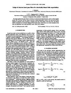
International Journal of Information and Electronics Engineering, Vol. 2, No. 4, July 2012
Design and Optimization of Band Pass Filter for Software Defined Radio Telescope Jolly Rajendran, Rakesh Peter, and K. P. Soman
paper, we describe the design, optimization and simulation of a coupled line microstrip bandpass filter with Chebyshev response. The design is simulated and optimized using ADS. The layout generated is simulated in Momentum.
Abstract—Design and optimization of a parallel-coupled microstrip bandpass filter for Software Defined Telescope is presented in this paper. The simulation and optimization is done using ADS and Momentum. The filter is designed and optimized at a center frequency of 1.42GHz. The filter is built on a relatively cheap substrate FR-4 with permittivity
II. DESIGN AND OPTIMIZATION OF CHEBYSHEV BAND PASS FILTER
r 4.4 and loss tangent tan 0.02 . Simulation results
Lowpass filter is the basic type of filters. Highpass, bandpass and bandreject filters can be achieved by frequency transformation of lowpass filter. Thus the synthesis of filter proceeds from tabulated lowpass filter prototypes. Chebyshev lowpass filter prototype is adapted in this paper because the attenuation of Chebyshev filter is steeper in amplitude versus frequency curve [1] and hence require only fewer stages for the same attenuation demanded. The microstrip filter specifications are as follows: 1) Equal ripple Chebyshev Filter response 2) Center frequency of 1.42 GHz 3) 3 dB bandwidth of 28.2% 4) Passband ripple of 0.5 dB 5) Passband attenuation 10 dB 6) Source Impedance = 50 Ohms 7) Relative permittivity of substrate ( r 4.4 )
reveal that the filter operation is optimum over the frequency range 1.41 GHz to 1.44 GHz. The 3 dB bandwidth is thus 300 MHz. the return loss is below -10 dB over the passband. Insertion loss is -2.806 dB in the passband. The filter is almost matched to the characteristic impedance ( Z 0 ), 50 Ohms. Also it is observed that the phase varies linearly with frequency. The filter once fabricated could be used at the radio receiver of the Software Radio Telescope to filter out terrestrial radio interference. Index Terms—Dielectric substrates, microstrip flters, microstrip band pass filter, chebyshev band pass filter, radio receiver, radio telescope, software defined radio telescope, optimization, ADS.
I. INTRODUCTION Stars, galaxies, quasars, and other astronomical objects are all cosmic radio sources. Radio telescope is used to study these cosmic signals. Software Defined Radio Telescope is a low cost telescope and could be used for educational purposes[3]. It consists of a radio antenna and a sensitive radiometer or radio receiver. Very often the cosmic signals received are weak and corrupted by terrestrial radio interference. The noise at the radio receiver is filtered out using a bandpass filter. The bandpass filter could either be realized using lumped components or distributed components. Lumped components consists of discrete elements like inductors, capacitors etc. Distributed elements consist of transmission line sections which simulate various inductance and capacitance values. It is hard to realize filters with lumped elements because at 1.42GHz, the dimensions of the electronic components are comparable with the wavelength of the signal as a result of which there could be distribute effects. However transmission line filters are easy to implement and are compact at this frequency. Hence transmission line approach is made use of in this paper. A bandpass filter allows transmission of frequencies in the passband and attenuates frequencies in the stopband. In this Manuscript received April 9, 2012; revised June 6, 2012. Jolly Rajendran is with the Department of ECE, Amrita Vishwa Vidyapeetham, Coimbatore, India (e-mail:
[email protected]). Rakesh Peter and K. P. Soman are with the Centre for Excellence in CEN, Amrita Vishwa Vidyapeetham, Coimbatore, India.
8) Thickness of substrate = 0.7 mm 9)
tan 0.002
A. Determining the Number of Sections (N) The bandpass filter is designed to have a 0.5dB equal-ripple response, with an attenuation of 30 dB at 1.47 GHz. From the amplitude versus normalized frequency graph in [1], the number of stages required, N is found to be 3. B. Determining the Value of Prototype Elements
Fig. 1. Bandpass filter using coupled lines.
Normalized element values for 0.5 dB ripple low-pass Chebyshev filter given in [1] was g0 = 1, g1 = 1.5963, g2 = 1.0967, g3 = 1.5963, g4 = 1.0000. The bandpass filter is realized as a cascade of N+1 coupled line sections as shown in Fig. 1. The sections are numbered from left to right. The source is connected at the left and the load is connected to the right. The filter could be reversed without affecting the response. C. Calculation of Odd and Even Resistances To design the microstrip filter, an approximate calculation
649
International Journal of Information and Electronics Engineering, Vol. 2, No. 4, July 2012
is made based on the design equations [5]. The no of stages (N) = 3. The characteristic impedance Z 0 is typically 50
E. Optimization in ADS The filter was modelled in ADS as shown in Fig. 3. The parameters of the substrate set in MSub controller are: 1) H: substrate thickness (0.7 mm) 2) Er: substrate relative dielectric constant (4.4) 3) Cond: metal conductivity (5.78E+6) 4) Hu: upper ground plane to substrate spacing (1.0e+33 mm) 5) T: the thickness of metal layer (0.35 mm) 6) TanD: dielectric loss tangent (0.002) 7) Rough: RMS surface roughness (0 mm). The filter dimensions are optimized using Genetic Algorithm. Optimization goals are set appropriately as shown in Fig. 3 and S parameter simulation is performed [4]. The new optimized dimensions of the microstrip line sections are listed in Table III.
Ohms. The unitary bandwidth BW is given by BW
U L 1.44 109 1.4 109 0.0282 1.42 109 C
(1)
The odd and even resistances are calculated by the following equations (2), (3) and (4) [1]:
1 J i.i 1 Z0
BW 2 gi gi 1
0.5
(2)
2 Z 0o |i ,i 1 Z 0 1 Z 0 J i ,i 1 Z 0 J i ,i 1
(3)
2 Z 0 e |i ,i 1 Z 0 1 Z 0 J i ,i 1 Z 0 J i ,i 1
(4)
TABLE I: CALCULATED VALUES OF EVEN AND ODD RESISTANCES.
TABLE II: CALCULATED DIMENSIONS OF TRANSMISSION LINE SECTIONS. Fig. 2. Determination of W. S and L linecale.
where i varies from 0 to N. According to the Equation (2), (3) and (4), the odd and even resistances of different stages are calculated as is shown in Table I. TABLE III: OPTIMIZED DIMENSIONS OF TRANSMISSION LINE SECTIONS.
D. Microstrip Line Modelling The length of each stage is chosen to be
g ( g
is the
guided wavelength), which corresponds to an electric length 0
(Eeff) of 90 . Using LineCalc tool in ADS, the dimension of the microstrip line viz. length (L), width (W) and gap(S) between each other are calculated for the given odd and even resistances at the design as shown in Fig. 2. Copper is used as conductor and FR4 with thickness 0.7 mm is used as substrate. The width, gap and length of each stage of the MCLIN (Microstrip Coupled-Line Filter Section) are derived, as illustrated in Table II. To match with the 50 ohm circuit, MLIN (Microstrip Line) components are added to both sides of the filter whose characteristic impedance is 50 ohms. The length and width of the transmission line section is found using the LineCalc tool as 29.2675mm and 1.34 mm [2].
F. Generating the Layout
Fig. 4. Filter layout.
The Layout of the filter is generated from the schematic design. The substrate features is specified. The layout of the filter is shown in Fig. 4. The simulation result in Momentum is shown in Fig. 5. The filter operation is optimum over the frequency range 1.41 GHz to 1.44 GHz. The 3 dB bandwidth is thus 300 MHz. the return loss is below -10 dB over the passband. Insertion loss is -2.806 dB in the passband. The filter is almost matched to the characteristic impedance ( Z 0 ), 50 Ohms. Also it is observed that the phase varies linearly with frequency.
Fig. 3. Band pass filter model in ADS.
650
International Journal of Information and Electronics Engineering, Vol. 2, No. 4, July 2012
G. Simulation Result in Momentum III. CONCLUSION The designed bandpass filter could be fabricated and used in the front end of SDR Radio Telescope [3]. Several interesting experiments could be carried out with this low budget Radio telescope. REFERENCES [1] [2]
[3]
[4] [5] Fig. 5. Simulated response of B.
651
D. M. Pozar, “Microwave Engineering,” 2nd ed New york, Wiley, 1998, pp. 367-368. Y. L. Hao, B. F. Zu, and P. Huang, “An Optimal Microstrip Filter Design Method Based on Advanced Design System for Satellite Receiver,” Proceedings of IEEE International Conference on Mechatronics and Automation, 2008. D. Morgan, “Experiments with a Software Defined Radio Telescope,” www.britastro.org/radio/projects/An\_SDR\_Radio \_Telescope.pdf, Accessed on: April 2012. “Tuning, Optimization and Statistical Design,” Agilent Technologies, May 2003. G. Mattaei, L. Young, and E.M.T. Jones, “Microwave Filters, Impédance Matching Networks, and Coupling Structures,” Artech House, Norwood, MA, 1980.