Mehrdad Biglarbegian, Neel Shah, Iman Mazhari and Babak Parkhideh. Department of Electrical and Computer Engineering. University of North Carolina at ...
Design Considerations for High Power Density/Efficient PCB Embedded Inductor Mehrdad Biglarbegian, Neel Shah, Iman Mazhari and Babak Parkhideh Department of Electrical and Computer Engineering University of North Carolina at Charlotte Charlotte, USA email: {mbiglarb, nshah49, imazhari, bparkhideh}@uncc.edu finding an alternative is very crucial. More specifically, due to the inverse relation of cutoff frequency with squared inductance and capacitance, air-core inductors with lower inductance could be a good option to substitute with ferromagnetic or magnetic cores [4]. Among various types of air-core inductors, PCB embedded ones potentially bring the benefit of miniaturization and integration to the power circuit [5]; however, these inductors due to their small surface area suffer from high resistivity and may not be used considering 1) stringent efficiency requirements and 2) desirable power density.
Abstract— This paper presents the design and implementation of high power density and highly efficient air-core embedded inductor onto Printed Circuit Board (PCB) for 280W-5A/240nH, 280W-12A/150nH and 280W-18A/50nH. The toroidal structure due to its better performance on interfacing electromagnetic fields (EMI), is investigated. In addition, thermal restrictions are considered at high current capacity by reducing the inductor size. This will bring the advantage of lower resistivity and consequently the conduction loss. Other challenges such as temperature rise optimization of high current (18A) on the PCB is also investigated. First, parameter calculation for design consideration of an embedded inductor are presented, then JMAG simulations are used to observe precisely the temperature rise profile distribution in different sections of the inductor. An optimized design to achieve high efficient inductor and simultaneously high power density is proposed and several experiments and accurate designs are shown. The primary results show an acceptable temperature rise for high current (18A) inductor without the heat sink.
(a) (b) (c) Fig. 1. Spiral (a), Solenoid (b), Toroid (c) the most common structures for aircore inductors
Keywords—PCB Embedded Inductor; high frequency; wide bandgap devices; high efficiency
I.
This miniaturization not only help us to mitigate the effect of parasites and unwanted interfaces with the other components of the circuits, it is also useful to reach high power density and achieve better transient performance [3],[6]. The various structures have been proposed for both embedded and non-embedded air-core inductors as shown in Fig.1. Solenoid, Spiral, Toroid are the most common structures to obtain the highest quality factor [5],[7]. Solenoid as shown in the Fig.1-b due to its rectangular structure can be easily implemented on the PCB and spiral as shown in Fig.1-a can be built on single layer bringing higher flexibility compared to toroid (Fig.1-c). Spiral and solenoid both have the potential to reach the higher inductance compared to toroid inductors, but their resistances are dramatically increased, and this causes lower quality factor specifically at high frequency. However, contrary of toroid solenoid and spiral are vulnerable to Electromagnetic Interfaces when they are nearby metallic elements on the circuit and this is the most important characteristic of toroid compared to the other proposed structures [5]. In this paper, the design procedure of the PCB embedded inductor with toroidal configuration to operate at high efficiency (more than 98%) for high frequency converters are
INTRODUCTION
To enhance the performance of the converters along with improving their efficiency and miniaturization in utility power electronics applications, a need for higher switching frequency is highly demanded. Although high frequency switching provides excellent opportunity to reduce the size of converters, due to the proportional relation of switching loss with increasing the frequency, the challenge of thermal dissipation needs to be addressed. At higher frequencies thanks to semiconductor developments such as GaN switches operating at 5-10MHz or Si-based AC-Stacked inverters operating at 500 kHz, the smaller inductor can be used for the AC filtering. By reducing the inductance, there is an opportunity to use aircore types instead of magnetic ones because of their lower costs and significantly lower losses at high frequencies; i.e. MPP cores are not suitable above 1MHz [1]-[2]. In many applications, ferromagnetic/magnetic-core inductors due to their high permeability, can help to confine the magnetic fields at low frequency; at higher frequency due to dramatic inductance variations, higher core losses and temperature rise restrictions, magnetics cannot bring any benefits [3], therefore
978-1-4673-7885-7/15/$31.00 ©2015 IEEE
247
By choosing low loss 1-2μ μF ceramic capacitor for the LC filter at the switching frequenccy below 10MHz, the 50-300nH range of the inductance will be desired.
proposed. Considering 2-5% power loss for the inverter stage, including conduction and switching lossees, the maximum allowable loss for the AC filter is set to be loower than 1-2% to achieve more than 95% efficiency for the invverter stage. Then, inverter design that can be used for PV appliications is targeted such that it can be operable with the avaiilable setup: rated power of 280W, 31.2V-DC voltage, 9.077A-DC current is selected and the inverter output AC currentt with 18A will be obtained.
In this paper, three differennt designs with relatively same quality factors for analyzing the temperature rise variations versus different switching freequencies are investigated. The inductance value of a toroidal PCB embedded can be calculated in (3) referring to [5]],[8]:
L= II.
N FOR THE PCB TEMPERATURE RISE FORMULATION EMBEEDEDD INDUCTOR
௱ூ
By assuming ripple current ratio ( ሻ and ripple output ூ
voltage ratio ( ሻ to be 1%, and duty cyclee of the switching frequency is lower than 70%, for the full brridge converter the inductance can be calculated through (1): f cutoff =
1 2π Lmin Cmin
=
1 4π
2
(Vin − Vout ) Dmax ΔIDmax m × ΔI × f sw
L ∝ μ0 kN 2 h + μ0α
(1)
(Vin − Vout ) Dmax 2 ΔV × f sw 2 × C
(4)
where, ߙ is the constantt factor and depends on the geometry of the inductor.
f sw ΔV
In this formula, ܦ௫ shows the maximuum duty cycle of switching pattern. Also, ݂௦௪ and ݂௨௧ are switching frequency and filter cutoff frequency, respeectively. Then, by simplifying:
L=
(3)
In this equation, ܰ definess the number of turns, ݄ shows the height of the inductor and ߤ is the permeability of the air. In addition, ݀ and ݀ show thhe inner and outer diameters of the toroidal inductor, respectivvely. In Fig.3 the geometry of the inductor have been shhown graphically. Practically, achieving a higher power density by miniaturizing the components due to increasinng the resistance brings some unwanted losses such as coppper conduction loss. In order to quantitatively demonstrate thee tradeoff between high power densities versus high efficieency in the PCB embedded inductor, the variable parametters for inductor design such as inductance, AC resistance, switching frequency of the converter and their correspondding effects on the temperature rise profile are presented. Thherefore, the inductance value proportionally can be correlateed to the variable parameters as shown below:
A. Inductance and AC Resistance Calculatioon In the range of 1-10 MHz, lower resistance of the PCB embedded inductor, not only helps to increase i electrical efficiency, but also does help to decrease the t thermal power loss dissipation and the temperature risee of the inductor simultaneously. Referring to (15), it is deesired to keep the quality factor of an inductor as high as posssible to reduce the conduction loss and increase the filterinng impact of the inductor. ௱
º N 2 h μ0 § d o · d o + di ª d +d ln ¨¨ ¸¸ + μ0 «ln(8 o i ) − 2» d o − di 2π 4 © di ¹ ¬ ¼
Upper Petal Input
(2)
Lower Petal
Vias
Output
Fig. 3. Defined geometric param meters of PCB embedded inductor
Based on [8],[9] the mostt challenging part to gain high efficiency for air-core inductorrs is resistance considering that the core loss has been eliminnated. Although, the resistance value at the toroid configuratiion is lower than other typical configurations [10], the thicknness of the board and the length of the inductor petal can effe fectively change the resistance. Here, (5), and (8) show resistance values in toroidal configuration [5]:
Fig. 2. Minimum inductance vs capacitance ratio at 5 & 10 MHz switching frequency for full bridge converter topology
248
§
RAC = N ¨¨ 2 × Rslab, AC + ©
Rslab , AC =
(6)
2 ρ × t PCB π × δ ( dVia − δ )
(7)
§
RDC = N ¨¨ 2 × Rslab, DC + ©
Rinner _ via _ DC Router _ via _ DC + N Inner Nouter
(9)
ρ × t PCB π × tVia ( dVia − tVia )
(10)
ΔTP.U = (
Q=
By considering these equations and applying iterative methods for finding the optimum parameters, we can obtain table-III to fulfill our requirements according to the primary specifications. In the first design, outer diameter has been selected 60-mm in order to increase the surface area for an effective heat dissipation. Then, by finding the minimum diameter of via, the inner diameter is calculated accordingly. In the further analysis, higher inductance value has been considered to increase the capability of heat dissipation along the petals. Despite increasing the inductance value, the ohmic losses will be raised and consequently makes the quality factor lower. Based on [8], AC resistance of the PCB embedded inductor can also be simplified as follows: N2 G0 − N ( β − 1)δ l
ωL Rac
ΔTP.U = =k
= k0
Q
)/(
Pbase UAbase
)
Q =1
(14)
= (
2π fL k1 2π fxN 2 = = k0 x f Rac k3 N 2 f
P ) UA
=k
Q
I 2Z I 2Z k = x2 × x f x3 f
I 2 (2π fL) 2 + Rac 2 x3
f
(15)
∝k
I 2 (2π fL) 2 + f
(16)
x3 f
I 2 ( f + α0 ) x3
Here, ݔis the ratio of surface area to the effective length that describes the inductor geometry; ܼ is the impedance, ܫis the rms current and ܳ defines the quality factor of the inductor. οܶǤ is temperature rise per unit of the quality factor for the inductor. Also, ݇ , ߚ , ߙ are the constant values after simplifying (12)-(16). Based on (16), the ratio shows that the temperature profile of the PCB embedded inductor by increasing the frequency will be increased as a function of ݂ ଵȀଶ ; correspondingly, the surface to length ratio needs to be scaled with ( ݂ ן ݔଵȀ ) to compensate the temperature rise variations on the PCB embedded inductor. Therefore, in the PCB embedded inductor design procedure, ݔas a degree of freedom representing the geometry of the inductor needs to be carefully chosen. In this paper, three different geometries with specific characteristics (as shown in table-III) are presented for precise evaluating the temperature rise variations at different ranges of frequencies and currents.
(11)
In (11), ܩ is the global conductivity, ݈ defines the average length of the current path and ߜ shows the skin depth of the copper in the inductor, which is associated inversely to the frequency (ߜ ି ݂ ןଵȀଶ ) as fully described in [8], therefore:
Rac ∝ k3 N 2 f
P UA
The temperature rise per unit of quality factor, which expressed in (14), gives the benefit to compare different design with the same quality factor to see the impact of effective filtering. Assuming the total power loss consists of only dissipative electrical power of the PCB embedded inductor, then the temperature rise per unit of quality factor can be correlated to the geometry of the inductor, continuous current of PCB embedded inductor and the switching frequency. According to the definition of quality factor [2] and by referring to (4) and (11):
In these equations, ߩ shows the electrical resistivity, ்ܥ defines the clearance of traces, ݎshows the inner and outer diameter of the slab,�்ݐ and ݐ are the thickness of the trace and via respectively.
Rac =
(13)
In this formula, ܲ is the total dissipative power of the inductors, ܷ is the global thermal coefficient and ܣis the global surface area for the PCB embedded inductor. Therefore, the overall temperature rise of the inductor is explained through the total dissipative power in the unit of surface area; To reduce the dissipative power by maintaining the quality factor, both inductance and resistance should be reduced; therefore, the temperature variations profile is redefined in (14) per unit of quality factor, as shown in:
· ¸¸ (8) ¹
§ 2π × router − CTrace × N · ρ×N ln ¨ = ¸ 2π × tTrace © 2π × rinner − CTrace × N ¹ Rvia , DC =
P = UAΔT
· ¸¸ (5) ¹
ρ × N § 2π × router − CTrace × N · ln ¨ ¸ 2π × δ © 2π × rinner − CTrace × N ¹ Rvia , AC =
Rslab , DC
Rinner _ via _ AC Router _ via _ AC + N Inner Nouter
(12)
B. Temperature Rise Calculation In natural thermal convection of the PCB embedded inductor to the environment, a generic equation to demonstrate the temperature rise of the components can be described as provided in [11]:
249
III.
turns/design-3 with 8 turns) of the PCB embedded inductors are proposed here. In the first model, the PCB embedded inductor with relatively big outer diameter-60mm and copper thickness = 35μm is designed. The goal of this design is to achieve high inductance to provide better filtering. Although this design has more surface area, we noticed that due to its high AC resistance and inductance the temperature rise at 5A is more than (35Ԩ). Therefore, it is not a proper choice for high power density applications; however, this design can lead to achieve effective filter especially for low frequencies due to its high inductance. In the second design, the inductor with the same outer diameter and copper thickness, but with lower number of turns (150nH) is implemented to tolerate the higher temperature rise; however, due to its relatively high AC resistance, the temperature of the inductor rises at 12A more would be more than 40Ԩ without using the heat sink.
DESIGN METHODOLOGY FOR THE PCB EMBEDDED INDUCTOR
As it mentioned before, the toroidal PCB embedded inductor has been selected to reduce the effect of EMI issues in the converter circuit design. The proposed geometry needs to be implemented at least in two-layer copper PCB, which are connected to each other through the vias. The current enters from input petal and can be circulated through the vias and the petals and then finally reaches to the output of the inductor (Fig. 3). In the design of the inductor, according to (1), the initial range of the inductance has been selected in the range of 50-300nH. According to (3), by increasing the number of turns, height and the outer diameter and decreasing the inner diameter of the PCB embedded inductor, it is possible to enhance its inductance for operating at wide ranges of frequencies and effectively filter out low frequency ripple current; however, increasing the number of turns, and outer diameter dramatically increase the DC/AC resistance, which results in more copper loss and poor efficiency. Therefore, taking to account all of the required parameters to acquire high frequency, PCB inductor leads to compromise higher efficiency and lower resistance. At high current applications, the most important challenges arise while the power dissipation of the PCB inductor increases because of the lower surface area and high resistivity.
a) 8-turn inductor (diameter 30-mm)
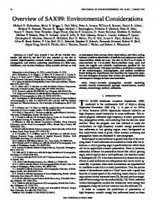
In this paper, in order to obtain the optimized geometry for operating at higher current with lower losses, JMAG simulation is used. As it is shown in (16), the temperature rise depends on the geometry, switching frequency and AC resistance. Therefore, by operating at higher frequency, the temperature will be increased with ( ݂ ןଵȀଶ ) and by optimizing the geometry and the physical parameters, the effect of the temperate rise cannot be easily compromised. Based on (11)(16), the temperature rise of the PCB embedded inductor can be changed by increasing the resistance of the vias and petals. The relevant parameters can effectively increase the AC resistance/ inductance, and accordingly the temperature rise. While operating in AC current, due to the presence of skin effect, the current intends to pass through the edge of the conductor. In addition, increasing the conductor surface area cannot decrease the AC resistance necessarily while operating at high frequency. As shown in (11), by increasing the number of via, the total resistance of the via will be decreased. In order to decrease the effect of resistance of the vias, optimization of the geometry are considered. For this purpose, different scenarios are proposed to reduce the resistance of the vias effectively. In these scenarios, different number of vias at inner and outer petals are compared to observe which parameter is more productive to reduce an AC resistance. This helped us for designing optimized PCB embedded inductors to reduce the resistivity and enhancing the current capacity. Furthermore, by changing the effective inner and outer diameters, the resistance of the vias were calculated and then verified through the simulations. Concurrently, various geometries with finite element methods have been simulated in JMAG. Then precise analysis of physical parameters such as inductance, resistance and the temperature rise to fully discover (16) are presented. Three different patterns (design-1 with 26 turns/ design-2 with 13
b) 13-turn inductor (diameter 60-mm) c) 26-turn inductor (diameter 60-mm) Fig. 4. Photograph of PCB inductor designs with (26 turns, 13 turns, 8 turns)
IV.
RESULTS
In the first and the second designs, the goal was to obtain the highest quality factor to operate at 5MHz switching frequency. Although, the designed inductors were suitable to filter the high frequency harmonics, due to their relatively high resistance, the temperature of the inductors rise rapidly. Therefore, a new model of inductor is proposed. We noticed in spite of lower surface area of the vias for conducting the current, the most critical part of the inductor, which makes higher resistivity of the copper is inductor petal. Because an alternative current tends to pass through the edge of the conductor, increasing the surface area of the petal as well as increasing the thickness of the copper helps reducing the losses and consequently intensify the ampacity of the inductor. In table I-II, the inductor resistance with different copper thickness are compared at 1 and 10 MHz. Furthermore, in various ranges of frequencies, the copper thickness increasing have been implemented, and the similar behavior at different spectrums were observed.
250
TABLE III. PHYSICAL PARAMETERS OF PCB INDUCTORS
TABLE I. COPPER THICKNESS EFFECTS ON AC RESISTANCE IN DIFFERENT GEOMETRIES OF THE INDUCTORS AT 1 MHz Frequency-1MHz
Design1
Design2
Design 3
Units
1-Oz 2-Oz 4-Oz 6-Oz
149.8 69.5 39.5 27.9
29.5 15 7.8 5.6
5.2 2.7 3 2.1
m m m m
TABLE II. COPPER THICKNESS EFFECTS ON AC RESISTANCE IN DIFFERENT GEOMETRIES OF THE INDUCTORS AT 10 MHz Frequency-10MHz
Design1
Design2
Design 3
Units
1-Oz 2-Oz 4-Oz 6-Oz
208.5 108 60.1 46.1
57.6 28.1 14.6 11
26.7 14.5 7.9 5.9
m m m m
Parameters
Design1
Design2
Design 3
Units
Inductance Number of Turns Outer Diameter Inner Diameter DC Resistance AC Resistance Via Diameter Height Surface to Length Ratio (x) Number of Via
242 26 60 20 160 200 1 1.5 7.5 76
150 13 60 20 32 50 2 3.5 7.5 37
50 8 30 15 2.4 8 2.8 3.5 6.8 22
nH mm mm m m mm mm cm -
According to the design, the resistance (Fig. 5) and the inductance (Fig. 7) in different ranges of frequencies are simulated and respectively the quality factor of each inductor is analyzed. Although, the inductance of the 8-turns PCB embedded inductor is much smaller than 26-turns, due to its specific design of the petals with low resistivity, the quality factor of the inductor improved. This means the temperature rise in the unit of the quality factor based on (16) can be restricted at higher frequencies. Fig. 6 shows how the quality factors of these inductors can be differentiated in various ranges of frequencies.
After further analysis of the changing the number of vias, it has been noticed that the number of via cannot practically change the resistance of the PCB embedded inductor. More specifically, the resistance of the inductor mainly is affected by the petal resistance, which directly will change the temperature rise. This comes from the fact that the thickness of the copper of the petals can effectively change the resistance of the PCB embedded inductor. In the third design, the goal is to reach out the highest achievable current simultaneously with the lowest conduction loss (outer diameter=30mm, copper thickness = 144μm resistance: 2.5m-DC and 8m-AC). Using this design, the optimized geometry is obtained such that the inductor can operate under 18A continuously with very low temperature rise. After analyzing different designs, the geometric parameters and physical parameter measurements are shown in table-III. By comparing this design with the bigger diameter inductors, an asymmetrical thermal distribution is observed in both simulation and experimental results as shown in Fig.8-10.
Quality Factor
350 300 250 200 150 100 50 0 1
2
3
4
5
6
7
8
9
10
Frequency (MHz)
Fig. 6. Quality factor of the three different designs vs. frequencies (orange: design-1: 26-turn, blue: design-2: 13-turn, gray: design-3: 8-turn)
Resistance vs. Frequency
250.00
Inductance vs. Frequency
300.00 250.00
200.00
200.00
150.00
150.00
100.00
100.00
50.00
50.00
0.00
0.00 1
2
3
4
5
6
Frequency (MHz)
7
8
1
9 10
2
3
4
5
6
7
Frequency (MHz)
8
9 10
Fig. 7. Inductance of the three different designs vs. frequencies (orange: design-1: 26-turn, blue: design-2: 13-turn, gray: design-3: 8-turn)
Fig. 5. Resistance of the three different designs vs. frequencies. (orange: design-1: 26-turn, blue: design-2: 13-turn, gray: design-3: 8-turn)
251
be prototyped. The theoretical analysis is demonstrated and three different geometries are designed in JMAG. The simulated inductors have been fabricated and the primary results are verifying the simulations. The 26-turn inductor with 240nH to operate at 5A and then, 13-turn inductor with higher efficiency in 12A current suitable at 5MHz switching frequency are proposed. Finally, an optimized design to operate at high current (18A) with very low resistance (DC: 2.5m/AC: 8m) which results in high power density/efficient toroidal PCB embedded inductor without using the heat sink is demonstrated. The current inductor can bring the benefit of integration and miniaturization of the passive filter for the high frequency wide band gap converters.
Fig. 8. The temperature profile of simulation and experimental results for (design-1: 26 turns, outer diameter = 60mm, copper thickness = 35μm, via diameter = 2mm, 242nH, 160m), I=5A, ambient temperaure 23Ԩ, asymmetrical thermal distribution is more significant due to its geometry, temperature gradient on the inductor petals is considerable on both simulation and experimental results.
REFERENCES [1] [2]
[3] [4]
Fig. 9. The temperature profile of simulation and experimental results for (design-2: 13 turns, outer diameter = 60mm, copper thickness = 35μm, via diameter = 2mm, 150nH, 32m), I=10A, ambient temperaure 23Ԩ, asymmetrical thermal distribution is more significant due to its geometry, temperature gradient on the inductor petals is considerable on both simulation and experimental results.
[5]
[6] [7] [8] [9]
[10] Fig. 10. The temperature profile of simulation and experimental results for (design-3: 8 turns, outer diameter = 30mm, copper thickness = 144μm, via diameter = 2.8mm, 50nH, 8m), I=18A, ambient temperaure 23Ԩ, asymmetrical thermal distribution is not significant due to its geometry and also temperature gradient on the inductor petals is insignificant compared to design-2 due to its smaller surface area and homogenous thermal distribution.
V.
[11]
CONCLUSION
In summary, this paper investigated the temperature rise profile of the toroidal PCB embedded inductor up to 10MHz switching frequency and presented an expression relating variable parameters such as current, frequency, and the inductor geometry to predict the temperature rise. Toroidal aircore inductor due to its higher performance with EMI issues and relatively low resistance at high frequencies is selected to
252
J. A. Mydosh, Handbook of Magnetic Materials, vol. 256, no. 1–2. 1997. D. J. Perreault, J. H. J. Hu, J. M. Rivas, Y. H. Y. Han, O. Leitermann, R. C. N. Pilawa-Podgurski, a. Sagneri, and C. R. Sullivan, “Opportunities and Challenges in Very High Frequency Power Conversion,” 2009 Twenty-Fourth Annu. IEEE Appl. Power Electron. Conf. Expo., 2009. P. Kamby, A. Knott, and M. a E. Andersen, “Printed circuit board integrated toroidal radio frequency inductors,” IECON Proc. (Industrial Electron. Conf., pp. 680–684, 2012. B. Mammano, “Resonant Mode Converter Topologies,” Power Supply Des. Semin. Unitrode, pp. 1–14, 1988. M. Madsen, A. Knott, M. a. E. Andersen, and A. P. Mynster, “Printed circuit board embedded inductors for very high frequency SwitchMode Power Supplies,” 2013 IEEE ECCE Asia Downunder, pp. 1071– 1078, Jun. 2013. J. R. Glaser, John, Wei Liang, “13 . 56 MHz High Density dc-dc Converter with PCB Inductors,” pp. 633–640, 2013. M. Ludwig, M. Duffy, T. O’Donnell, P. McCloskey, and S. C. Ó Mathùna, “PCB integrated inductors for low power DC/DC converter,” IEEE Trans. Power Electron., vol. 18, no. 4, pp. 937–945, 2003. C. R. Sullivan, W. Li, S. Prabhakaran, and S. Lu, “Design and Fabrication of Low-Loss Toroidal Air-Core Inductors,” 2007 IEEE Power Electron. Spec. Conf., pp. 1754–1759, 2007. S. Orlandi, B. Allongue, G. Blanchot, S. Buso, F. Faccio, C. Fuentes, M. Kayal, S. Michelis, and G. Spiazzi, “Optimization of shielded PCB air-core toroids for high efficiency dc-dc converters,” 2009 IEEE Energy Convers. Congr. Expo., pp. 2073–2080, Sep. 2009. D. Brooks and D. Graves, “Current Carrying Capacity of Vias Some Conceptual Observations,” no. January, 2003. T. L. Bergman, A. S. Lavine, F. P. Incropera, and P. Dewitt, Heat and Mass Transfer. 2011.