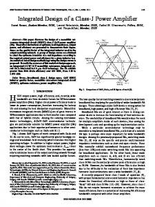
IEEE MICROWAVE AND WIRELESS COMPONENTS LETTERS, VOL. 16, NO. 2, FEBRUARY 2005
81
High-Efficiency Power Amplifier Design Including Input Harmonic Termination S. Gao, P. Butterworth, S. Ooi, and A. Sambell
Abstract—This letter presents the design of a high-efficiency Class-F power amplifier in pseudomorphic high electron mobility transistor technology using a novel load-pull/source-pull simulation-based approach. The second harmonic input termination is shown to have a critical influence on performance, which is justified by the shape of the simulated waveforms. Experimental validation is carried out on a 2-GHz practical circuit using a medium-power packaged device. Two cases are compared both theoretically and experimentally: for the best and worst case second harmonic input terminations, 76% and 42% saturated power-added efficiency are measured, respectively. In addition, the worst case termination degrades the saturated C/I3 by 7.5 dB. Index Terms—Class-F, harmonic tuning, high-efficiency, power amplifier (PA).
output loads of the transistor taking into account all device nonlinearities and parasitic effects. Experimental validation is carried out on a 2-GHz printed circuit board (PCB) circuit using a medium-power packaged device. The board uses a specific circuit configuration, allowing practical measurement of the best and worst case second harmonic input terminations obtained by simulation, which are found to be high reflection-coefficients with negative and positive phase, respectively. The measured PAE at 3-dB compression drops from 76% to 42% with 21-dBm output power as the second harmonic input load is changed from the best to the worst case termination, in good agreement with simulation. II. DESIGN METHODOLOGY
I. INTRODUCTION
A. Principle
H
IGH-POWER-ADDED efficiency (PAE) is one of the key requirements in today’s radio frequency (RF) and microwave power amplifiers (PAs). To achieve it, it is necessary to drive the active device heavily into compression, leading to highly nonlinear behavior. Specific design schemes, based on switching mode such as Class-E, or on harmonic manipulation such as Class-F [1], [2] or its dual Inverse Class-F, can be used. The characteristics of these different high-efficiency modes are best appreciated by observing the shape of the voltage and current waveforms at the output of the active device, which in turn largely defines the performance of the PA. Most theoretical analyses for high-efficiency PAs are based on output only models. As a consequence, the available literature emphasizes the critical importance of the output load of the transistor, but often overlooks the effect of the input harmonic termination. Nevertheless, the second harmonic input termination has been shown experimentally to have a significant influence on efficiency [3]–[6] and linearity [3], [6], demonstrating the need to integrate it into the design process. It has been suggested that the optimum second harmonic input termination for Class-F PAs is close to a short circuit [3], [4], but it has not been made clear how the precise optimum load can be predicted. This letter proposes a simulation-based design methodology for high-efficiency PAs, which allows effective and precise optimization of the input and
Manuscript received July 27, 2005; revised October 24, 2005. This work was supported by the Engineering and Physical Sciences Research Council (EPSRC) under Grant GR/S42538/01. The review of this letter was arranged by Associate Editor F. Ellinger. The authors are with the Active Antenna Group, School of Computing, Engineering and Information Sciences, Northumbria University, Newcastle Upon Tyne NE1 8ST, U.K. (e-mail:
[email protected]). Digital Object Identifier 10.1109/LMWC.2005.863171
The proposed design methodology uses a load-pull/sourcepull approach to find the input and output optimum harmonic loads of the active device at the first three harmonic frequencies. The approach, which is simulation-based, is an extension of the one proposed in [6] for experimental device characterization. The obvious advantage of using a simulation approach is that the need for an expensive multiharmonic load-pull/source-pull experimental setup as well as time-consuming and potentially troublesome measurements is alleviated. Instead, the process is carried out with a commercial harmonic-balance (HB) simulator using a nonlinear model for the active device. A further benefit of the approach is that it allows direct visualization of the intrinsic voltage and current waveforms, meaning the performance of the active device can be easily and precisely assessed. The complete characterization of a device’s power performance, given fixed frequency and bias conditions, requires the exploration of a multivariable space with six complex spacestate variables corresponding to the input and output harmonic loads at the first three harmonic frequencies. Non-linear optimization schemes must overcome problems such as trapping in local minima, which lead to suboptimum results or simulation convergence limitations, which are frequent at high drive levels. Hence, a direct optimization method is not seen as a very effective means of obtaining the desired optimum harmonic loads. In the proposed load-pull/source-pull methodology, the statespace variables are varied one at a time in a determined order based on relative importance and reported interactions, leading them to be successively adjusted to their optimum values. B. Simulation Setup The harmonic loads (Fig. 1) are initially set to their ideal values, i.e., for a Class-F amplifier, the output second and third
1531-1309/$20.00 © 2005 IEEE
82
IEEE MICROWAVE AND WIRELESS COMPONENTS LETTERS, VOL. 16, NO. 2, FEBRUARY 2005
Fig. 1. Load-pull/source-pull simulation setup.
TABLE I SIMULATED OPTIMUM HARMONIC LOADS FOR PAE
Fig. 2. Simulated PAE contours for the input second harmonic (ZS ).
harmonic load and are set to short- and open-circuits, respectively, whereas the other harmonic loads are set to 50 . First, a fundamental load–pull simulation is performed; is varied to sweep meaning that the complex output load is set to the determined optimal the Smith chart. Second, value and is swept by source–pull simulation so as to fix it to its optimum value. At this stage, it is necessary to reoptimize to take into account the influence of the new [6]. The , , and are then sucremaining harmonic loads cessively swept and set to their optimum values. Throughout is adjusted the process, the fundamental source impedance automatically for each simulation point to achieve a conjugate match of the input impedance of the device, thus maintaining a constant drive level. C. Simulation Results The methodology was applied to a medium-power packaged pseudomorphic high electron mobility transistor (pHEMT) transistor (ATF-34 143 from Agilent Semiconductor). The Statz nonlinear model provided by the foundry was corrected based on previous practical measurements results [2], [7] to improve its PAE prediction capacity. The device is biased for 3-V drain bias in deep Class-AB mode leading to a quiescent current of Idss/7, which corresponds to a gate bias of 0.5 V. Simulation is performed at 2 GHz, taking into account a practical grounding inductance of 0.16 nH, for an input power of 8 dBm corresponding to 3-dB gain compression. The obtained optimum impedances for PAE, which take into account all device parasitics and the interactions between input and output nonlinearities, are given in Table I. As can be seen, the final output harmonic loads differ significantly from the ideal has a very strong influence, as shown in the sourceones. pull plot in Fig. 2; the optimum load represented by point a 1.5 j21 leads to a PAE of 77%, whereas PAE degrades to less than 45% at point b 1.2 j21 . The corresponding input intrinsic voltage waveforms are compared in Fig. 3. The waveform observed for point b, featuring a strong negative spike and a turn-on duty cycle much higher than 50% is due to the strong nonlinearity of the gate capacitance of pHEMT transistors around pinch-off. It is known to have detrimental effects on device efficiency, linearity and reliability [4], [5]. In contrast, the quasisinusoidal input waveform observed
Fig. 3.
Simulated intrinsic gate voltage waveforms.
Fig. 4. Simulated intrinsic drain waveforms.
for point a is suitable for Class-F operation. The output waveforms (Fig. 4) show a 50% duty cycle and minimal overlap between the intrinsic output voltage and current waveforms, which results in high-efficiency performance. It is obtained by pro1.5 j21 , viding an input second harmonic load which short-circuits the second harmonic of the intrinsic gate voltage given the inductive parasitics of the packaged device. III. EXPERIMENTAL VALIDATION A. Circuit Realization To verify the simulation results, a practical circuit was fabri2.33) substrate (Fig. 5). cated on 0.79-mm thick Duroid ( Matching circuits are synthesized to provide the desired impedances to the active device at the fundamental and first three harmonics at the input and output. Biasing is performed using a 4 transmission line shorted by a second-harmonic resonant chip capacitor (C1) at the drain and by a 4 line shorted by a 4 open stub at the gate. The optimum second harmonic terminations, high-reflection coefficients with negative imaginary parts, are provided by shifting a short-circuit with series transmission lines of slightly less than 4 length at the fundamental frequency. The second harmonic shorts are provided by the drain bias circuit at the output, and by a 8 stub at the input. A further 8 line in the gate bias
GAO et al.: HIGH-EFFICIENCY POWER AMPLIFIER DESIGN
83
Fig. 7.
Fig. 5. Photo of fabricated circuit, dimensions: 94 mm
2 nm.
Measured carrier over third-order intermodulation ratio (C/13).
CW PAE and gain performance of the circuit. In configuration a, a peak PAE of 76% together with 13-dB gain is achieved at 3-dB compression, whereas in configuration b, the peak PAE is only 42% with similar output power. Fig. 7 shows the measured third-order intermodulation ratio (C/I3) at 2 GHz with 100-kHz tone spacing. The linearity performance of both configurations is similar in small signal with an output third-order Intercept (IP3) of 30.5 dBm, but it degrades faster as the circuit is driven into compression in configuration b. The difference in C/I3 reaches 7.5 dB in saturation. IV. CONCLUSION
Fig. 6.
Single-tone gain and PAE performance.
circuit, shorted by a resonant chip capacitor at the second harmonic (C2) ensures the load brought back by the gate bias line at the second harmonic is controlled. Moreover, the second harmonic input termination can be changed experimentally to the by connecting a negligible worst case simulated load value chip resistor 1 to the open stub labeled b in Fig. 6. The stub is slightly less than 8 long to compensate for the extra inductance added by the connecting chip. At the output, the third harmonic load is provided by a short length open stub, whereas both input configurations provide the desired open. Finally, a good match is achieved at the fundamental both at input and output. The topology ensures that connecting stub b does not directly influence the input match. However, the second harmonic termination does affect the input impedance of the device, meaning the input return loss is slightly degraded at 10 dB in configuration b, from 15 dB in configuration a. B. Measured Performance The circuit was measured at 2 GHz in single- and two-tone modes, in the configurations corresponding to the a) best and b) worst case second harmonic input loads. Fig. 6 represents the
The design of a high-PAE Class-F amplifier in pHEMT technology, using a simulation-based load-pull/source-pull methodology, has been presented. Experimental results at 2 GHz in excellent agreement with simulation confirm the importance of performing second harmonic input tuning. Two cases are compared both theoretically and experimentally. For the best and worst case terminations, 76% and 42% saturated PAE are measured, respectively. The design approach is also further applicable to optimization of other PA performances such as output power or intermodulation distortion. REFERENCES [1] S. Gao, “High-efficiency class-F RF/microwave power amplifiers,” IEEE Microw. Mag., to be published. [2] P. Butterworth, S. Gao, S. F. Ooi, and A. Sambell, “High-efficiency class-F power amplifier with broad-band performance,” Microw. Opt. Technol. Lett., pp. 243–247, Feb. 2005. [3] M. Maeda, H. Masato, H. Takehara, M. Nakamura, S. Morimoto, H. Fujimoto, Y. Ota, and O. Ishikawa, “Source second-harmonic control for high-efficiency power amplifiers,” IEEE Trans. Microw. Theory Tech., vol. 43, no. 12, pp. 2952–2958, Dec. 1995. [4] P. M. White, “Effect of input harmonic terminations on high-efficiency class-B and class-F operation of PHEMT devices,” in IEEE MTT-S Int. Dig., 1998, pp. 1611–1614. [5] K. Jeon, Y. S. Kwon, and S. C. Hong, “Input harmonics control using nonlinear capacitor in GaAs FET power amplifier,” in IEEE MTT-S Int. Dig., 1997, pp. 817–820. [6] P. Colantonio, F. Giannini, E. Limiti, and V. Teppati, “An approach to harmonic load- and source-pull measurements for high-efficiency PA design,” IEEE Trans. Microw. Theory Tech., vol. 52, no. 1, pp. 191–198, Jan. 2004. [7] Agilent Technologies, Tech. Rep., Available: http://literature.agilent.com/litweb/pdf/5988-4210EN.pdf, 2005.