accommodate future standards such as IEEE 802.20 Mobile. Broadband Wireless Access (MBWA) systems. REFERENCES. [1] T. Fujitsawa et al., A Single-Chip ...
Design methodology for memory-efficient multi-standard baseband processors Anders Nilsson, Eric Tell, Daniel Wiklund and Dake Liu Div. of Computer Engineering at Department of Electrical Engineering, Linkoping University, Linkoping, Sweden E-mail: {andni,erite,danwi,dake}@isy.liu.se
Abstract— Efficient programmable baseband processors are important in order to enable true multi-standard radio platforms and software defined radio systems. In programmable processors, the memory sub-system accounts for a large part of both the area and power consumption. This paper presents a methodology for designing memory efficient multi-standard baseband processors. The methodology yields baseband processor micro-architectures, which eliminate excessive data moves between memories while still allowing true flexibility by utilizing SIMD clusters connected to memory banks via an internal network. The methodology has successfully been used to create a multi-standard baseband processor for OFDM-based wireless standards. This paper discusses the IEEE 802.16e (WiMAX), DVB-H (Digital Video Broadcast - Handheld) and DAB (Digital Audio Broadcast) standards. The architecture is truly scalable to accommodate future OFDM systems. Scheduling and resource allocation show that with the proposed memory structure and architecture, the processor can manage the baseband functions of the described standards operating at 80 MHz and using only 28k words of memory.
I. I NTRODUCTION In future radio systems, multi-standard signal-processing capability will be increasingly important. To support a large amount of different standards, programmable baseband processors are necessary since ASIC solutions are not flexible enough. Furthermore, ASIC solutions for multi-standard baseband processing are less area efficient than their programmable counterparts since processing resources cannot easily be shared between different operations. Generally the memory sub-system accounts for a large portion of both the area and power consumption in digital signal processing systems [1]. It is important that the memory architecture balances bandwidth against the access rate to reduce the overall power and area cost for the memory subsystem. In order to reduce power consumption in the processor it is also important to ensure that the data are accessible in the right memory. This will eliminate unnecessary data moves between memories. This paper presents a design methodology for multistandard baseband processors and a base architecture, which the methodology uses. The base architecture consists of a DSP controller core, flexible SIMD execution units, and a memory system interconnected by a memory crossbar switch. The methodology and the base architecture are demonstrated by mapping several OFDM-based radio standards to
this processor architecture. This paper considers three different standards: IEEE 802.16e [2], DVB-H [3] and DAB [4]. All baseband functions such as synchronization, channel compensation, and frequency/timing-offset cancellation have also been taken into account when firmware tasks have been analyzed and mapped to the processor. The base architecture are optimized for vector oriented baseband processing rather than single operations unlike other programmable architectures [1], [5], [6]. This solution is based on memory tiles, which are connected to the execution units through a memory crossbar switch. Instead of moving data between memories, data memories are reconnected to the appropriate input port of the corresponding execution unit. The paper is organized as follows: In section II the design methodology are presented. The methodology utilizes a base processor architecture, which is presented in section V. In section VI the design methodology are applied to the discussed standards, and results are presented in section VII. Conclusions are drawn in section VIII. II. D ESIGN METHODOLOGY In order to create an efficient baseband processor architecture, both in terms of memory usage, area, and power efficiency, a methodology has been developed that consists of the following steps: 1) Analysis and high-level modeling of the application and algorithm selection. 2) Mapping of the selected algorithms to a base architecture. 3) Benchmarking and analysis of the algorithms on the architecture to find limiting factors on memory usage, memory access rate, latency requirements and computing capacity. 4) Selection of memory sizes, memory organization and width of the execution units. 5) Selection of accelerators (if needed). All of the steps above must be performed for all considered radio standards that should be supported by the architecture. By creating an architecture that supports the worst load in all corners of the design space, this will ensure architectural support for new and diverse standards, which fall inside the limitations imposed by the worst case. The goal of the design methodology is to find parameters to the base architecture such as:
Required clock frequency. Memory size and number of memory banks. • Required execution units. (E.g. ALU and CMAC) • Number of lanes in the execution units. The memory organization will follow the number of lanes in the execution units in order to fulfill memory access requirements. • Which accelerators to use. In the first stage of the methodology, a high level model is used to find all kernel functions used in the standards. These kernel functions will then be mapped to components in the base architecture framework. Information about processing deadlines and maximum allowed latency is also extracted from either the simulation models or the standard specification in this stage. • •
III. A NALYSIS PHASE To aid the analysis of the mapping of the selected baseband processing algorithms onto the base architecture, two important factors must be considered: MIPS cost and maximum allowed computing latency. These two factors will be considered for all kernel operations encountered during the first stage of the methodology. A. MIPS cost In order to compare the computational load of a certain algorithm, we define MIPS cost, which corresponds to how many million instructions per second a regular DSP processor would require in order to perform the specified function. The MIPS cost is calculated as follows: M IP Si =
OPi ·Ni ti
where M IP Si is the associated MIPS cost, OPi the number of clock cycles required by a standard DSP processor to perform the operation, Ni the number of samples or bits to process and ti is the maximum time allowed for the operation to complete. The time to perform the operation is usually considered to be one symbol time. This metric indicates the approximate computing complexity of an algorithm or operation. Since the time allowed for an operation to complete is dependent on scheduling, the MIPS cost analysis and scheduling must be iterated until a satisfying solution is found. B. Latency In most OFDM based systems there are three factors limiting the computing latency: • Channel equalization. In a packet-based system, the channel estimation performed on the preamble must be complete before the processing of the user payload symbols is started. • High level acknowledge packets. In time division duplex systems and TDMA systems such as WLAN and WiMAX the standard stipulates the maximum allowed time from the end of a received packet to the beginning of the transmitted response packet. • User delay. User protocols such as voice services limit the overall latency in a communication system.
IV. C OMPONENT SELECTION When the baseband tasks have been analyzed both in terms of latency requirements and MIPS cost, the results can be used to select vector execution units, memories, and accelerators. A. Vector execution units To ensure efficient execution of all kernel functions, we utilize vector execution units. Analysis of general OFDM signal processing reveals that all associated kernel functions are based on convolution, vector multiplication and FFT. Convolution, vector multiplication and FFT can be performed on a multi-lane MAC unit. As a response to this we need flexible and efficient vector execution units mainly focused on MAC functionality. To increase the processing parallelism and maintain a high computing efficiency, we propose the use of multi-lane MAC units. A multi-lane MAC unit can easily be extended to perform a FFT butterfly each clock cycle [7]. The MIPS cost and memory access rate yielded from the analysis of the worst-case load will be used to select the number of lanes in the execution units. The width of the execution units will be a trade-off between circuit area (more memories are needed in higher radix circuits) and desired clock rate. The total number of memory accesses must also be taken into account when selecting execution units since this has a large impact on power efficiency. B. Memory organization The number of memory banks is mainly determined by the chosen task level parallelism whereas the width of each bank is determined by the memory bandwidth required by the execution units. A radix-2 compatible MAC unit needs to read three complex data items and write two complex data items each butterfly operation during FFT calculations. A radix-4 unit will on the other hand require a total of 11 memory accesses per butterfly operation. C. Accelerators When deciding which functions to accelerate the following must be must considered: 1) MIPS cost. A function with a high MIPS cost may have to be accelerated if a regular processor cannot perform the operation. 2) Reuse. A function that is performed regularly and is used by several radio standards is a good candidate for acceleration. 3) Circuit area. Acceleration of special functions is only justified if there can be considerable reduction of clock frequency or power compared to the extra area added by the accelerator. An operation that fulfills one or more of the previous points is a good candidate for hardware acceleration.
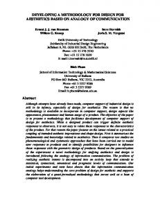
V. BASE ARCHITECTURE To aid the design methodology, a base architecture has been used that serves as a framework to which we add components such as memories and execution units. A complete baseband processor consists of two main parts, one baseband processing part that mainly operates on vectors of complex numbers and one scalar part that operates on integers and single bits. The latter part is mainly used for forward error correction (FEC) and bit manipulation whereas the former part is used to extract soft data symbols that can be de-mapped into bits. However, since bit manipulation and FEC tasks are so diverse from baseband processing we limit ourselves to the baseband functionality in this paper. An efficient multistandard architecture for acceleration of bit manipulation and FEC tasks is presented in [8]. The base architecture consists of memory banks connected to execution units via a memory crossbar switch. The architecture is shown in Figure 1.
M
M
M
M
Memory crossbar EX
EX
EX
Execution units
M
M
...
ACC
...
Control bus
AGU / Memory control ADDR
ADDR
ADDR
ADDR
Memory 0
Memory 1
Memory 2
Memory 3
DO
DO
DO
DO
DI
M
On chip network EX
Memory bank #n
Mux control
Scalar memory banks Vector/scalar bridge
Complex valued "vector" memory banks
unit before a vector instruction is issued and then operates autonomously during the vector operation. The AGU of each memory bank can either operate in normal, bit-reversed or modulo mode. The memory bandwidth can be increased by dividing each memory bank into several parallel memories. To enable the possibility to access all individual memories from a single port of the memory bank, we introduce a reordering crossbar switch. This crossbar switch allows any single memory to be accessed from any of the ports. This feature is especially useful when the memories are written by a single port device such as the mapper or the analog interface. Later, the memory content can be accessed in parallel in order to facilitate higher radix based algorithms and transforms.
DI
DI
Reordering crossbar
4 complex data out ports
ACC
DI
Fig. 2.
4 complex data in ports
Example of a 4-way memory bank.
Execution units and accelerators
Complex oriented baseband part
Fig. 1.
Bit/Scalar oriented part (FEC, Scrambling, et.c)
Base architecture.
The crossbar allows any memory to be connected to any execution unit. Execution units span the range from a DSP controller core, to multi-lane complex MAC and ALU SIMD data-paths. Accelerators such as an analog front-end and mapper/de-mapper together with a network bridge to the scalar part of the processing system are also attached to the memory crossbar. The base architecture relies on the observation that most baseband processing tasks operate on a large set of complexvalued vectors (such as auto-correlation, dot-product, FFT and convolution). This allows us to use vector instructions, i.e. a single instruction that triggers a complete vector operation such as a complex 128-sample dot product. To support this kind of vector instructions, the execution units must be able to process large data chunks without any intervention from the processor core. This in turn requires the execution unit and memory sub-system to have automatic address generation and efficient load/store subsystems. As a response to this, the base architecture utilizes de-centralized memories and memory addressing together with vector execution units. A. Memory banks Since the architecture relies on de-centralized memory addressing, each memory bank has an associated address generator unit (AGU). The controller core configures this
B. Task level pipelines By using several memory banks connected to the memory crossbar switch, all execution units can operate in parallel. This allows the architecture to support “task level pipelines”. Task level pipelining is a method of increasing the processing parallelism by running several independent jobs simultaneously and passing data between the jobs at specific times. This technique is also used to store incoming samples in one memory while other execution units operate concurrently. When a processing task is finished the memory banks are reconnected so that the output memory buffer from an execution unit is connected to the input port of the next execution unit in the processing chain. This memory arrangement allows the base architecture to perform all OFDM reception and transmission tasks without any data moves between memories. VI. A PPLICATION OF THE METHODOLOGY Following this methodology, high-level models of the discussed standards have been developed and kernel functions have been derived. The kernel functions have been analyzed both in terms of resource usage and latency requirements according to the methodology. To be able to correctly account for all memory accesses, operations and data dependencies, the reception algorithms of OFDM systems have been analyzed with respect to memory usage, memory access rates, latency requirements, and memory access patterns according to the methodology. Since reception is more computationally demanding than transmission, we only consider reception tasks in this paper. Baseband reception tasks of OFDM data consist of the following steps[9]:
• • • • • • • • • •
Packet/frame detection. Synchronization. Frequency error estimation/tracking. Frequency error correction and decimation/filtering. Channel estimation/tracking. Guard period removal. FFT. Phase tracking and correction. Channel correction. De-map.
Tasks such as packet/frame detection and synchronization are only performed when the receiver initially searches for a valid OFDM packet or frame. The second task group is preformed on every received sample whereas the last group is performed on every received data symbol. Analysis and implementation of the reception tasks in the table above reveal three kernel operations which are frequently used: • Complex FFT is used to transform time domain data into frequency domain data. The FFT is also used for cyclic correlation when performing synchronization. • Complex MAC is used for dot-product calculations. • Complex vector multiplication is used for channel compensation and cyclic correlation.
access rate for FFT operations can be significantly reduced. Since the dynamic power consumption of CMOS circuits and memories is proportional to the clock frequency and access rate, it is beneficial to increase the processing parallelism to reduce the required clock frequency and lower the memory access rate. One way to increase the processing parallelism is to utilize Radix-4 butterflies in the FFT. A Radix-2 FFT of length N uses N2 log2 N butterflies compared to N4 log4 N butterflies for Radix-4. When single cycle Radix-4 butterflies are used to increase the processing parallelism, the memory sub-system needs to manage eleven memory transactions each clock cycle for the FFT in addition to the memory transactions needed for other concurrent operations. B. Memory banks By analyzing the kernel operations required in OFDM reception and all data dependencies, it can be shown that four memory banks of the same size as the received data symbol including guard period are sufficient in a flexible baseband processor. Latency requirements for all the discussed standards impose a limit, which requires all symbol processing tasks to be executed within a symbol period. A mapping of the IEEE 802.16e OFDM standard onto the architecture described in Figure 4 is presented in Figure 3. Memory DM0 DM1
A. Vector execution units To ensure the efficiency of a baseband processor, all kernel functions need to run as efficiently as possible. Since the base architecture assumes execution units which can sustain one operation per clock cycle, the memory access rate can be used as a measure of the MIPS cost. In Table I the number of memory accesses are listed together with each operation. Since the discussed standards have many different modes, the most demanding has been used for this analysis. TABLE I OVERVIEW OF MEMORY ACCESS RATES AND PARAMETERS Operation FFT Channel comp. De-map
IEEE 802.16e 6144 op 768 op 256 op
DVB-H 147456 op 12288 op 4096 op
DAB 67584 op 6144 op 2048 op
Symbol length: (incl. max GI): Symbol duration: (incl. GI): Avg. access rate:
320 pts
5120 pts
2560 pts
23.15µs
462µs
1246µs
309 MHz
354 MHz
60 MHz
In the previous table, a radix-2 based FFT calculated in a single multiplication unit is assumed. In practical signal processing circuits there are a few different efficient methods of calculating a FFT (or its inverse). Most common are techniques utilizing hardware which could perform a radix-2 or radix-4 butterfly in one clock cycle. As described in section IV-A the radix of the execution units is a trade off between area and access rate. By using a radix-4 FFT butterfly, the memory
DM2 CM
Symbol #n
Symbol #n+1
11101000 000 111000 111 00001000 111 111000 111 111 000 000 111000 111 111 000 000 111000 111 111 000 111 000 000 111 111 000 Reception of symbol #n
Reception of symbol #n+1
FFT
Phase tracking and correction
Fig. 3.
Demap
Channel compensation
Memory scheduling for OFDM reception.
The memories are scheduled as follows: 1) DM0: Used to store incoming symbols. 2) DM1: Used as source for calculations. 3) DM2: Used as destination of calculation results. 4) CM: Used as coefficient memory for calculations and for storage of constant vectors. This scheme and the memory crossbar switch eliminate the need for memory moves. A possible design alternative is to use a dual-port memory instead of the two data memories that are reserved for computations. However, since the power consumption and the area for a double-port memory is roughly twice of a single port memory, we are only considering single port memories. The overhead due to many small memories must also be considered against both the required memory access rate and data access patterns. C. Accelerators Of the symbol processing tasks, four tasks are selected to be implemented as accelerators: The packet detector, frequency error compensation, filtering/decimation, and mapping/demapping. These four tasks fulfill all requirements for implementation as an accelerator. They are also used among all
Memory bank 0
Sample Memory
Memory bank 1
Sample Memory
AGU
Memory bank 2
Filter and pulse−shaping
Analog front−end
CMAC
CMAC
CMAC SIMD Data path
Fig. 4.
VII. R ESULTS Application of the presented methodology on the three discussed standards yields the following architecture parameters: 1) Four memory banks of totally 28k words of memory. 2) A radix-4 compatible CMAC unit. 3) Acceleration of front-end tasks and mapping/demapping. 4) A controller core with scalar data-paths. The resulting multi-standard OFDM processor architecture is presented in Figure 4 and the memory requirements are presented in Table II. The maximum performance figures are related to the IEEE 802.16e standard whereas the maximum memory requirement is derived from the most memory demanding standard, DVB-H, which uses up to 5120 samples per symbol that are stored alternately in DM0 and DM1. TABLE II O RGANIZATION OF MEMORY BANKS Organization 2048x32 2048x32 1024x32 2048x32
CMAC
ALSU
MAC
Controller unit
Map/ demap
Network Interface
Network bridge
To/From scalar on−chip network
Resulting processor architecture
discussed standards and can be efficiently implemented in hardware.
Total area 0.92 mm2 0.92 mm2 0.51 mm2 0.92 mm2
In Table III peak memory power consumption and access statistics are presented for main receiving tasks in IEEE 802.16e implemented on this architecture. TABLE III C YCLE AND MEMORY ACCESS COSTS Operation 256 pts FFT Ph. tracking and comp. Ch. comp. De-map
AGU
RF
Vector load/store unit
Frequency error cancellation CMAC
Amount 4 4 4 4
Sample Memory
AGU
Memory cross−bar switch (5 x 4 port groups)
Port groups
Bank DM0: DM1: DM2: CM:
Sample Memory
AGU
Memory bank 3
Clock cycles 256 264
Accesses per cycle 11 1
Memory power 48 mW 4 mW
Energy 154 nJ 14 nJ
256 64
3 4
12 mW 16 mW
42 nJ 13 nJ
Area and power figures are collected from commercially available memory generators for a standard 0.13µm digital
CMOS process. Mapping and simulations yield a maximum required clock rate of only 80 MHz when the presented architecture runs reception tasks of the discussed standards. This maximum operation frequency is a result of latency requirements of the IEEE 802.16e standard which specifies the longest turnaround time between two packets. VIII. C ONCLUSIONS The main focus of this paper has been to present a design methodology together with an efficient base architecture which yields memory efficient programmable multi-standard OFDM baseband processors. The proposed base architecture increases the memory efficiency and reduces the memory power consumption by using de-centralized addressing and vector execution units. By eliminating unnecessary moves between memories and reducing the required clock frequency of the processor, power can be saved while maintaining full flexibility. This architecture is also scalable to easily accommodate future standards such as IEEE 802.20 Mobile Broadband Wireless Access (MBWA) systems. R EFERENCES [1] T. Fujitsawa et al., A Single-Chip 802.11a MAC/PHY with a 32b RISC Processor, ISSCC Dig. Tech. Papers, pp. 144-145, Feb. 2003. [2] IEEE Standard for local and metropolitan area networks, Part 16: Air Interface for Fixed Broadband Wireless Access Systems. WirelessMANOFDM [3] ETSI EN 300 744, Digital Video Broadcasting. DVB-T/DVB-H [4] ETSI EN 300 401, Radio broadcasting systems: Digital Audio Broadcasting to mobile, portable and fixed receivers. [5] J. Kneip et.al. Single Chip Programmable Baseband ASSP for 5 GHz Wireless LAN Applications, IECICE Trans. Electron., vol.E85-C, N0.2 February 2002. [6] J. Glossner et al, A Software-Defined Communications Baseband Chip, IEEE Communications Magazine, January 2003. [7] Eric Tell, Olle Seger and Dake Liu; A Converged Hardware Solution for FFT, DCT and Walsh Transform; Proc. of the International Symposium on Signal Processing and its Applications (ISSPA), Paris, France, Vol. I, pp. 609 - 612, July 2003 [8] Anders Nilsson, Eric Tell and Dake Liu, An Accelerator Structure for Multi-Standard Programmable Baseband Processors, Proc. of IASTED Intl. Multi-Conf. on Wireless and Optical Com., pp 644-649, July 2004 [9] H Heiskala and J T Terry, OFDM Wireless LANs: A Theoretical and practical guide, Sams Publishing, 2002