Design Space Exploration for Aggressive Core Replication Schemes in CMPs Lluc Alvarez∗†
[email protected] Xavier Martorell∗ †
[email protected] ∗
Ramon Bertran∗ †
[email protected] Nacho Navarro∗ †
[email protected]
Barcelona Supercomputing Center C. Jordi Girona, 29 08034 Barcelona, Spain
†
Marc Gonzàlez∗ †
[email protected] Eduard Ayguadé∗ †
[email protected]
Departament d’Arquitectura de Computadors Universitat Politècnica de Catalunya C. Jordi Girona, 31 08034 Barcelona, Spain
ABSTRACT
Design, Performance
The trend in the HPC domain is to use CMPs but it is not clear what is the best CMP design for this environment. In order to find the CMP configuration that better fits in the HPC domain it is important to know its applications’ characteristics. In general, HPC applications are parallel computational loops which operate on huge data sets that are sequentially traversed, exposing a high degree of task-level parallelism and data-level parallelism. These characteristics seem to fit better in architectures with a high number of cores because they are able to take more profit of this high degree of parallelism. Following this observation and the trend opened by the design of the Intel SCC [1] this paper studies the behaviour of CMP configurations that sacrifice the size of the shared cache in order to have more area to perform an aggressive core replication. On the one hand, having more cores has the immediate consequence of being able to execute parallel loops faster. On the other hand, this schemes can have important drawbacks: the lack of scalability of cache coherence protocols [2] limit the number of cores, and reducing the size of the L3 cache increases its miss ratio and so generates off-chip traffic, so a higher bandwidth is required. This paper studies all these implications on different chip configurations in terms of number of cores, size of the shared L3 cache and off-chip bandwidth requirements.
Keywords
2. ARCHITECTURE AND DESIGN SPACE
Design Space Exploration, Chip Multiprocessor
A CMP is composed of num cores cores, a shared L3 cache of size L3 size and an interconnection network that connects these components. The chip uses a bus with a bandwidth of BW for off-chip communication. In order to obtain realistic configurations, it has been defined two parameters α and β. The parameter α corresponds to the relation between the area of 1MB of L3 cache and the area of a core. The parameter β is defined as the minimum amount of memory in L3 cache per core. Given a baseline chip configuration and a pair of values for α and β one can derive new chip configurations by reducing L3 size and increasing num cores avoiding undesired chip configurations, since α keeps the area of the chip constant and β imposes a balance between the number of cores and the L3 cache. To fix values for α and β floorplans of modern architectures such as IBM POWER7, Intel Nehalem and AMD K10 have been examined. Following this observations, the values used for α are 0.25, 0.33 and 0.5, while for β they are
Chip multiprocessors (CMPs) are the dominating architectures nowadays. There is a big variety of designs in current CMPs, with different number of cores and memory subsystems. This is because they are used in a wide spectrum of domains, each of them with their own design goals. This paper studies different chip configurations in terms of number of cores, size of the shared L3 cache and off-chip bandwidth requirements in order to find what is the most efficient design for High Performance Computing applications. Results show that CMP schemes that reduce the shared L3 cache in order to make room for additional cores achieve speedups of up to 3.31x against a baseline architecture.
Categories and Subject Descriptors C.1.2 [Processor Architectures]: Multiple Data Stream Architectures (Multiprocessors); C.1.4 [Processor Architectures]: Parallel Architectures; C.4 [Performance Of Systems]: Design Studies, Performance Attributes
General Terms
1.
INTRODUCTION
Chip multiprocessors (CMPs) are the dominating architectures nowadays and, probably, in the future. CMPs are used in a wide spectrum of domains: high performance computing (HPC ), servers, commodity desktops, gaming, embedded systems, etc. The majority of CMP designs are based on the replication of several cores inside the same chip sharing up to some degree a complex memory subsystem. However, current CMPs present a big variety in their organizations because the optimal chip configuration highly depends on several design goals such as performance, energy consumption, scalability, area and programmability. Copyright is held by the author/owner(s). HPDC’11, June 8–11, 2011, San Jose, California, USA. ACM 978-1-4503-0552-5/11/06.
269
Table 1: Chip configurations.
α
6MB 8 cores 48MB L3 8 cores 48MB L3 8 cores 48MB L3
0.25 0.33 0.5
4MB 10 cores 40MB L3 10 cores 40MB L3 10 cores 40MB L3
2.5
2MB 13 cores 26MB L3 14 cores 28MB L3 16 cores 32MB L3
β
1MB 16 cores 16MB L3 18 cores 18MB L3 21 cores 21MB L3
3.0
3.5
2.5
1.0
2.0
SPEEDUP
SPEEDUP
SPEEDUP
2.0 1.5
1.5
1.0 0.5
0.0
8 cores 48MB L3 10 cores 40MB L3 13 cores 26MB L3 20
16 cores 16MB L3 17 cores 8.5MB L3 18 cores 4.5MB L3
35 50 BANDWIDTH (GB/s)
65
256KB 18 cores 4.5MB L3 22 cores 5.5MB L3 28 cores 7MB L3
3.0
2.5
2.0
512KB 17 cores 8.5MB L3 20 cores 10MB L3 25 cores 12.5MB L3
8 cores 48MB L3 10 cores 40MB L3 14 cores 28MB L3
0.5 0.0
1.5
1.0
20
(a) α = 0.25
18 cores 18MB L3 20 cores 10MB L3 22 cores 5.5MB L3
35 50 BANDWIDTH (GB/s)
65
8 cores 48MB L3 10 cores 40MB L3 16 cores 32MB L3
0.5 0.0
20
21 cores 21MB L3 25 cores 12.5MB L3 28 cores 7MB L3
35 50 BANDWIDTH (GB/s)
(b) α = 0.33
65
(c) α = 0.5
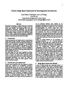
Figure 1: Speedup of the different CMP configurations.
25
40
20
15
10
35 30
55
120 cycles 180 cycles 240 cycles 300 cycles 360 cycles 420 cycles 480 cycles
50 REQUIRED BANDWIDTH (GB/s)
REQUIRED BANDWIDTH (GB/s)
30
45
120 cycles 180 cycles 240 cycles 300 cycles 360 cycles 420 cycles 480 cycles
REQUIRED BANDWIDTH (GB/s)
35
25 20 15
8 cores 48MB L3
10 cores 40MB L3
13 cores 16 cores 17 cores 26MB L3 16MB L3 8.5MB L3 CHIP CONFIGURATION
(a) α = 0.25
18 cores 4.5MB L3
10
45 40 35
120 cycles 180 cycles 240 cycles 300 cycles 360 cycles 420 cycles 480 cycles
30 25 20 15
8 cores 48MB L3
10 cores 40MB L3
14 cores 18 cores 28MB L3 18MB L3 CHIP CONFIGURATION
20 cores 10MB L3
22 cores 5.5MB L3
10
8 cores 48MB L3
10 cores 40MB L3
(b) α = 0.33
16 cores 21 cores 25 cores 32MB L3 21MB L3 12.5MB L3 CHIP CONFIGURATION
28 cores 7MB L3
(c) α = 0.5
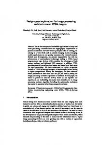
Figure 2: Bandwidth requirements of the different CMP configurations.
4. CONCLUSIONS
6MB, 4MB, 2MB, 1MB, 512KB and 256KB of L3 cache per core. The baseline chip configuration used is a CMP with num cores = 8 and L3 size = 48MB. This baseline chip configuration is used as the starting point to derive new chip configurations combining values of α and β. The resulting chip configurations are shown in Table 1. The values for BW have been derived from the HyperTransport technology, fixing them to 20GB/s, 35GB/s, 50GB/s and 65GB/s.
3.
This paper explores the design space of CMPs in order to find an efficient design for HPC applications. The design space exploration contemplates design parameters such as the number of cores, the size of the shared L3 cache and the bus bandwidth. The study analyzes the performance and the required bandwidth of different chip configurations and what is the impact of varying each design parameter. Results show that aggressive core replication is very beneficial when the available bandwidth is very high. Configurations that reduce the L3 cache to 256KB per core and use the free space to put more cores achieve speedups of 2.13x, 2.58x and 3.31x with a bus of 65GB/s when compared to a baseline CMP architecture with 8 cores and 48MB of L3 cache.
EVALUATION
Figure 1 shows the average speedups of every CMP configuration with respect to the baseline architecture. Aggressive core replication schemes achieve maximum speedups of 2.13x, 2.58x and 3.31x depending on α. These best three chip configurations are obtained with β = 256KB and a provided bandwidth of 65GB/s. In this figure it can also be observed the scalability of CMPs, which is perfect when β ≥ 1MB and, after that point, reducing the L3 cache to add more cores provide under-linear speedups because the L3 cache miss ratios start to increase significantly. Figure 2 shows the average required bandwidth by the different configurations with several main memory latencies. For chip configurations with β ≥ 1MB the average required bandwidth grows linearly due to the addition of cores. When β < 1MB the miss ratios increase and so the bandwidth requirements do, showing a super-linear growth in the three plots. In all cases the average required bandwidth is acceptable, with a maximum of 51.2GB/s.
5. ACKNOWLEDGMENTS We thankfully acknowledge the support of the HiPEAC2 Network of Excellence (FP7/ICT 217068), the European commission, the Spanish Ministry of Education (TIN200760625 and CSD2007-00050), the Generalitat de Catalunya (2009-SGR-980) and the BSC-IBM MareIncognito project.
6. REFERENCES
[1] The SCC Platform Overview. Revision 0.7. May 24 2010. [2] A. Ros, M. E. Acacio, and J. M. Garc´ıa. Parallel and Distributing Computing, chapter Cache Coherence Protocols for Many-Core CMPs, pages 93–118. IN-TECH, Janyary 2010.
270