Amit Chowdhary and Dinesh Bhatia. Design Automation Laboratory. ECE Department. University of Cincinnati. Cincinnati, OH 45221-0030. Abstract. We present ...
Detailed Routing of Multi-Terminal Nets in FPGAs Amit Chowdhary and Dinesh Bhatia Design Automation Laboratory ECE Department University of Cincinnati Cincinnati, OH 45221-0030
Abstract
router results in a small channel width by considering the side-effects of routing of one connection on another. One drawback of the CGE router is that each multi-terminal net is decomposed into a group of two-terminal nets before routing. This may result in an excessive routing delay if the final route of this multi-terminal net has the output pin on one end. The signal will then have to travel a long distance t o reach an input pin on the other end. This is further aggravated if the number of input pins in the net is very large. In fact, we have found a few nets in the industrial circuits t o have as many as 20 t o 30 input pins. We have designed a router that addresses this problem by placing an upper bound on the length of the route from the output pin of a multi-terminal net to any input pin on the same net. This bound is the m i n i u m possible, which is the distance between the output pin and the input pin on the same net and farthest from the output pin. This results in the final routed circuit with very low routing delay even in the worst case. The architecture of an LCA is described in the next section. Section 3 describes the main features of our router. Section 4 gives a detailed description of our router. The results of our router are presented in section 5. The concluding remarks are in the last section.
We present a multi-terminal routing algorithm for fieldprogrammable gate arrays (FPGAs). The routing problem for the FPGAs is dificult due to the preplaced routing segments that can be connected only by the pre-existing switches. We describe a sequential router that routes multiterminal nets in a single stage, i.e., global routing is not required. The multi-terminal routing greatly reduces the total ware length as the multi-terminal tree approximates the steiner tree as opposed to a minimum cost spanning tree. Our router requires very small channel width. In addition, our router places an upper bound on the worst case delay by routing a multi-terminal net within its bounding box. Within the bounding box each terminal is routed in a distance that is less than or equal to the max(l(i,o)), where o is an output pin, i is a n input pin, and l(i, 0) is the Manhattan distance between an input and output pin. Our router has generated excellent routing results for some of the industrial circuits.
1 Introduction Field-Programmable gate arrays (FPGAs) are becoming popular for implementing Application Specific Integrated Circuits (ASICs). Our study addresses the problem related with routing in an FPGA architecture called logic cell arrays (LCAs). The architecture is very popular and has been pioneered by Xilinx [8]. This type of FPGA has preplaced wiring segments in the horizontal and vertical channels. The segments can be connected using programmable switches for making long connections or for introducing bends. The predefined routing architecture makes the detailed routing problem for FPGAs far more difficult than the traditional detailed routing [7, 41. Brown et. al. [2] have developed a detailed router for LCAs that routes the two-terminal nets within their assigned global routes. The router, known as the Coarse Graph Expansion (CGE) router, expands the global route (coarse graph) of each net t o find a detailed route. This
2
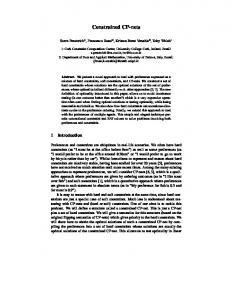
Architecture of an LCA
The architecture of the logic cell array is shown in figure 1. An LCA is a two-dimensional array of logic blocks. Each logic block has 7 pins: pins 0 - 3 are the input pins, 4 is the clock pin, 5 is the tri-state pin and 6 is the output pin. Each pin appears on only one side of the logic block. For details refer t o [6]. The LCA also consists of horizontal and vertical routing channels. Each channel consists of sections, that span the length of one logic block. The channel sections are represented by their type (horizontal or vertical), row number and the column number. The routing switches are present in the connection boxes and switch boxes. A connection box or C box consist of switches that
7th lntematlonal Confenrnce on VLSI Design -January 1994 231
0-81864990-9/94$3.00 Q 1994 IEEE
pose each multi-terminal net into a group of two-terminal nets, perform the global routing of two-terminal nets and then route the circuit within the global routes using a detailed router. The search space for finding a detailed route is restricted to the assigned global route. Our router operates on the netlists obtained after the placement and pin assignment. It does not decompose nets into two-terminal nets nor does it require global routes. Some of the main features of our router are listed below.
InpWoutpuI Block
Each input pin on a net is routed in such a way that the length of the route from the output pin to the input pin is never more than the distance between the output pin and the input pin farthest from it. This places an upper bound on the length of the route between the output pin of the net and any of its input pin. All the input pins in a net lying on the critical path can be routed t o the output pin in the beginning with the shortest possible distance. This results in a final routed circuit with a low routing delay.
SwitchBlock
Figure 1: Architecture of Logic Cell Array
The input pins of a net are routed in the decreasing order of their distance from the output pin of that net. As more and more pins on a net are routed, the routed portion of that net increases, so the probabdity of routing the subsequent input pins also increases. This is because the later routes can merge with the previously routed paths more easily to form a steiner tree. This compensates for the increase in the difficulty of routing due to a large number of routing resources already used.
Figure 2: The Flexibility of Switch and Connection Boxes connect the logic block pins to the wiring segments. The switch box or S box switches connect one wiring segments to another. The S boxes are present on the intersection of the horizontal and vertical routing channels. The flexibility of a C box, F,, is defined as the number of segments to which each logic block pin can be connected. The flexibility of an S box, Fs,is defined as the number of segments to which a wiring segment entering a S box can be connected. This LCA architecture is very similar to the one used in [l]and we have used the same terminology for F, and F,. The flexibilities of C and S boxes are shown in figure 2. From now on, we will use the terms FPGA and LCA interchangeably.
The storage requirements of our router are very small.
Our router takes in the topology of the switch box and the connection box (i.e. the pattern of the switches) as an input. The topology of a switch box specifies all the pairs of segments on different sides of the box that can be connected by programmable switches. Similarly, the connection box gives the location of the switches inside that box.
4 3
Main Features of the MultiTerminal Sequential Router
Terminology
4.1
Before giving a detailed description of the routing algorithm, we define the following terms.
The input t o the router is in the form of a netlist obtained after the placement and pin assignment. Each multi-terminal net has one output pin and one or more input pins. From now onwards, a net will refer to a multiterminal net, unless specified otherwise. The aim for routing the nets is t o achieve 100% routing with the channel width and the routing delay as low as possible. Besides this, the memory storage and the execution time requirements of the router should be kept low. The approach normally followed for routing is t o decom-
Maz-Length(i) : This is the distance between the output pin and the input pin farthest from the output pin for the net i , where 1 5 i 5 N , N being the total number of nets. Current-Route(i) : This is the partial route of the net
This includes the output pin and a subset of input pins of net i alongwith the wiring segments used for routing these input pins.
a.
238
1
The Router Algorithm
DITAILED GRAPH
Figure 3: The complete and the final global graph of an input pin (partially shown)
O
The no&a stand for
scgmsntrr and the edgea etimd forth switohes
Complete-Global-Graph : This is a directed acyclic ) Vc is a subset of channel graph C G ( V C , E C where sections and there exists an edge between two nodes vi and v j ifE iand j are adjacent channel sections. CG is constructed each time an input pin belonging to net i is routed to its Current-Route(i). The input pin to be routed is the root node and has in-degree equal to zero. For each input pin, it consists of Max-Length(i) levels, where level j consists of all the channel sections that are a t a distance j from the root node. The Complete-Global-Graph of a channel section is shown in the figure 3.
Figure 4: The detailed graph obtained b y expanding the global graph in the previous figure (partially shown)
FinaEGlobal-Graph ; This is a subgraph (FG(VF,E F ) ) of Complete-Global-Graph. VF is a collection two types of nodes. (1) A node v1 belongs to VF,if the channel section represented by 01 contains a segment that belongs to Current-Route(;). (2) A node v2 belongs to VF, if it lies on a directed path from the root node to any one node belonging to VF,. VF = VF, U VF,. EF is a subset of edges belonging to Ec such that each edge - is incident to a node in V F . The Final-Global-Graph corresponding to a Complete-Global-Graph is shown in figure 3.
4.3
belonging to the critical path are arranged in descending order of their distance from the output pin of that net followed by the remaining pins in the same order. This should not be mistaken as two terminal decomposition. Here we are arranging input pins in the decending order of distance from the output pin for each net seperately. Thus for N nets, we will have N seperate sets of sequences.
Routing of nets
We now describe the algorithm for routing the nets in a sequential manner. The outermost loop is executed Mazpins number of times since in every iteration one input pin from all the nets is routed. In the first iteration, for each net the input pin from the top of the pin sequence is routed to the output pin of that net. Afterwards, the subsequent pins are routed to the already routed portion of the net given by Current-Route. This algorithm is executed twice for a better performance'. The routed portion of a net is small in the early stages of the routing. Thus, a few of the input pins in the beginning of the pin sequence might not get routed. These pins may get routed in the second pass, since the routed portion of the net increases in size after the completion of the fist pass.
- -
5 . Detailed-Graph : The Detailed-Graph (DG(VD,E D ) ) is obtained by expanding each channel section in the FinabGlobal-Graph into individual wiring segments. DF is also directed acyclic graph where VD represents a wiring segment within a channel segment and there exists an edge between v 1 and v2 iff vi and v 2 belong to adjacent channel sections and share a programmable switch between them in the switchbox. Figure 4 shows the detailed graph obtained after expanding the final global graph of figure 3.
4.2
M ailer oxpanding the ~lobalgraph in the previous f m .
Preprocessing of nets 'In fact the algorithm can take multiple passes. In each pass it will attempt to route some pins to their respective current routes. As the execution progresses the current route portion of each net also grows end thus the probability of successful routing would also increase.
Each net has One Or more input pins and an Output pin* Let Maz-pins denote the number Of input Pins in any net. The input pins of each net are arranged in a sequence such that a t the start, all the input pins
239
Procedure ROUTE; begin While the input pin sequence of a l l the nets is not empty For each net i The bmr drawn by thedoted lines is t h e d o n box. The switches in the comedon bon sre marked by ‘x’.
Pop the first pin from the top of the input pin sequence of that net.
Figure 5: The relevant portion of the grid for determining the cost of any segment an the channel section
Construct the Complete- Global- Gr aph with this input pin as the root node.
between the two switch bozes
Extract the Final-Global-Graph from the Complete-Global-Graph.
2. SegConnectiwity[SegNo][SideNo] : As seen from the figure 5 , a segment in a channel section can connect
Expand into the Detailed-Graph.
to segments in six different channel sections through two switch boxes. SegConnectiaitll[SegNo][SideNo] stores the number of segments in one of these six channel segments (given by SideNo) to which a segment (given by SegNo) can be connected. Initially, the value of this parameter depends solely on the topology of the switch box. If a segment is used in routing, its connectivity becomes zero. For each segment used in routing, the connectivity of all the segments in the six channel sections shown in Figure 5 will need t o be updated.
Select the minimum cost sink node. { Select the leaf node of the Detailed-Graph that is of minimum cost. Trace back from the sink node till the root node is reached to get the path with minimum cost. Include minimum cost path in the Current-Route(i).
1 Update the cost function. { Update the cost of all the segments. Remove the routed input pin from the pin sequence.
If a segment in a channel section can connect t o a large number of segments in the adjoining channel sections or a large number of pins in the same section, then the cost of that particular segment must be high since it is in a great demand. Also, if a segment in a channel section can connect to segments in adjoining channel sections or pins in same section that can in turn connect to only a few alternative segments in the channel section of the segment in question (i.e. they have a low connectivity in that section), then that particular segment must have a high cost. All these facts are taken into account while designing the cost function given below.
1 End For End While end;
4.4
Cost
Function
Each segment in the FPGA has a certain cost assigned to it. The cost assigned t o a segment reflects the demand of that segment. The cost of any route is the sum of the cost of all the segments on it. We define following terms to describe the cost function.
1
-I-
SideNo EdgeNo
SegConnectivity[EdgeNo][SideNo]
Here, the summation over EdgeNo is done for a l l the segments in the adjoining sections that can be connected to the segment SegNo. Similarly, the summation over PinNo is done for all pins in the same section that can be connected to the segment in question. The weight assigned to the cost of a segment due to the pins is taken t o be four times of the weight of the cost due to the segments in the adjoining sections. This is motivated by the fact a pin can get out through only
1. PinConnectiwity[PinNo] : This stores the number of unused wiring segments t o which the pin, specified by PinNo, can be connected to. Its initial value depends on the flexibility and the topology of the connection box. After a pin is routed, the connectivity of the routed pin becomes zero. The connectivity of some other pins may decrease by one if they can be connected t o a segment that has been used in the recent route.
240
5.1
one channel section, while a segment in a section can be connected t o segments in six different sections.
4.5
Time Complexity and Memory Requirements of the Router
Our router can be used as a global router for FPGAs by keeping the the switch box flexibility F, and the connection box flexibility F, as the maximum possible. In this case, the maximum channel density over all the channels for a circuit or simply the channel density will be the lower bound on the number of segments required to complete the detailed routing of that circuit. The channel density for a circuit also reflects the quality of the router used. The channel density for the industrial circuits using our router are shown in table 11. This channel density is compared with the density obtained after global routing by a modified version of the LocusRoute global router [5] as stated in [2]. As seen from the table, the channel density obtained by our router is almost the same as that reported by Brown et. al. [2]. Thus, our router gives good results in terms of the channel density required to route the circuits.
L e m m a 1 The multi-terminal detailed router has a time complexity of O ( K M 2 W F , ) and requuires O ( M 2 W ) storage space, when the size of and LCA is M x M ,the channel width is W , and K is the total number of input pins in the circuit. The time complexity of this routing algorithm is governed by the expansion of the global graph into a detailed graph. The global graph has O ( M ) levels and each level has O ( M ) number of channels. Each channel has W segments, where each segment can connect to order F. segments in the next level. Thus, the expansion of global graph into a detailed graph takes O ( M z W F s ) time. This step is performed for all the input pins in the circuit thereby making the overall timecomplexity t o be
Table I1 Channel d e n s i t y after global routing
O(KM2WF,). The memory requirements of our router depends on two data-structures: storing the detailed graph for the input pin being routed and storing the routes of the nets. The detailed graph has O ( M ) levels and each level has O ( M ) channels with each channel having W segments. Thus the memory required for storing a detailed graph is of O ( M 2 W ) .For storing the routes of all the nets, the memory required is of O ( M 2 W ) ,since each segment can be on at most one net and total number of segments is O ( M 2W ) .
5
Channel Density after Global Routing
BNRE 203
11
12
As explained before, the multi-terminal routing requires lesser number of segments compared to the two-terminal routing. Table IV shows that the total number of used segments for routing a circuit using the sequential router with maximum possible flexibility of the connection box and the switch box is about 8 - 15% less than the number of used segments in the global routes obtained by LocusRoute global routing algorithm [5]. Above all, as explained before, our router bounds the routing delay.
Results
Our router has been used t o route several industrial circuits on FPGAs as shown in table I. These circuits are from different sources: Bell Northern Research (BNR) , Zymos and two different designers at University of Toronto (UTD1 & UTD2). The idea behind routing these particular circuits was t o compare with the results of the CGE router [2]. The CGE router [2] is a detailed router only and so an adaptation of LocusRoute global routing algorithm [5] has been used by Brown et. al. for global routing of the circuits in [2].
5.2
Channel Width after Detailed Routing
The industrial circuits are routed using the sequential router with the flexibility of switch box F, equal to 6 and that of the connection box F, equal to 0.6W. The channel width W obtained after routing the circuits using the sequential router is compared with the CGE router [2] and the maze router [3] in table 111. Our sequential router requires more or less the same number of segments as required by the CGE router [2], but is far better than the ordinary maze router [3]. At any stage, the sequential router does not have any knowledge about the subsequent terminals to be routed. The advantage of this is that the memory and time requirements are quite low compared t o the CGE router [2].
Table I
241
I
Channel width W required ( F , = 6; F, = 0.6W)
I
CGE
I
Our
1
Maze
12 203
5.3
13
13
18
I
coude of segments more than an existing- parallel router. We strongly believe that the channel width can be further reduced by using a more efficient topology of the switch box and the connection box. This router can also be used to design better routing architectures for the FPGA. It can be used as a global router only, since the total number of segments used is quite small and the routing delay is also very low. Another attractive feature of this router is that the memory requirements depend only on the space needed for storing the routes and hence is quite small. The speed of routing is very fast even for very large FPGAs. Finally, the router is also independent of the routing architecture of the FPGA. I
CPU
116 141 231
Total number of used segments
Table IV shows the total number of segments used for routing the circuits. For F, = 6 and Fc = 0.6W, the total net length in terms of the number of the used segments ,obtained by the sequential router is slightly less than that obtained by the CGE router [2].
7
Acknowledgments
The authors would like to thank Jonathan Rose and Stephen Brown of the University of Toronto for providing us the code of the CGE router and the benchmark circuits.
Table IV
References Stephen Brown. Routing Algorithms and Architectures for Field-Programmable Gate Arrays. PhD thesis, University of Toronto, 1992.
5.4
Time and storage requirements of the sequential router
Stephen Brown, Jonathan Rose, and Zvonko Vranesic. A Detailed Router for Field-Programmable Gate Arrays. IEEE Transactions on Computer-Aided Design, 11(5):620-627, May 1992.
The memory required by the sequential router is between 100 and 500 Kbytes, as opposed to the CGE router [2] that needs about 1.5 - 7.5 Mbytes of memory. The time taken by the sequential router lies between 8 t o 231 seconds aa shown in table 111. The execution time needed by the router is the CPU time taken on a Sun SPARC-2 work-station. It should be stressed that our router eliminates the global routing stage. Thus, the time required by our router should actually be compared with the time needed for the detailed as well as the global routing using other approaches.
6
C. Lee. An algorithm for path connections and its applications. IEE Transactions on Electron. Comp., EC-10:346-365, September 1961.
B. Preas and M. Lorenzetti. Physical Design Automation of VLSI Systems. Benjamin Cummings.
J. Rose. Parallel global routing for standard cells. IEEE Transactions on Computer-Aided Design, 9:1085-1095, October 1990. Jonathan Rose, Robert J. Francis, David Lewis, and Paul Chow. Architecture of Field-Programmable Gate Arrays: The Effect of Logic Block Functionality on Area Efficiency. IEEE Journal of Solid-state Circuits, 25(5):1217-1225, October 1990.
Conclusions
We have designed a sequential router for logic cell arrays that has a bounded delay in a final route. Our router eliminates the need of the global routing stage. Since the detailed routes of the nets have a steiner tree type of configuration, the total number of segments required to route the complete circuit is usually less than any other routing approach. Even though it is a sequential router, the channel width required for routing the circuits is very less
[7] J. Soukup. Circuit layout. In Proceedings of IEEE, volume 69, pages 1281-1304, Oct. 1981. [8] Xilinx Inc., San Jose, California. Gate Array Data Book, 1992.
242
The Programmable