Institute of Physics Publishing doi:10.1088/1742-6596/15/1/029
Journal of Physics: Conference Series 15 (2005) 172–176 Sensors & their Applications XIII
Development and application of a neutron sensor for singleevent effects analysis S P Platt, B Cassels and Z Torok Department of Technology, University of Central Lancashire, Preston, Lancashire. PR1 2HE Email:
[email protected] Abstract. The development and application of a charge-coupled device (CCD) sensor for neutron detection is described. The sensor provides images of neutron-induced single-event effects (SEEs) at 9 µm pixel resolution and a charge/pixel resolution of typically 36.6 electronic charges. Example results are presented, showing the charge profiles resulting from single events observed during tests in a representative neutron spectrum. The sensor enables aspects of SEE phenomena to be studied directly in more detail than hitherto.
1. Single event effects in electronics Interactions between semiconductor electronic devices and energetic subatomic particles, such as neutrons, can adversely affect device performance in several ways. In particular, interaction with individual particles can disrupt the function of a device through spurious charge generation, sometimes also leading to permanent failure through a range of indirect mechanisms including latch-up. These effects are termed “single event” effects (SEEs) as each results stochastically from a single interaction between a device and an ionising particle, rather than occurring as the cumulative effect of many interactions [1]. Neutrons, although not directly ionising, induce SEEs through nuclear interactions with constituent ions of the semiconductor lattice. Technology trends in electronic systems and components are leading to greater susceptibility to single event effects [2]. Smaller device structures, lower operating voltages, and higher clock speeds result in a greater likelihood of device disruption by SEEs, especially in environments where the radiation environment is hostile. One such environment is the atmosphere at altitude, where a damaging neutron flux, arising from the effects of cosmic radiation, is found [3]. As a result, neutroninduced SEEs are of particular concern in avionic applications [4]. To ensure reliability, ground testing of avionic components is routinely undertaken at neutron test facilities such as the TriUniversity Meson Facility (TRIUMF), located at the University of British Columbia, Vancouver [5]. This facility provides a simulation of the atmospheric neutron spectrum with neutron flux approximately six orders of magnitude greater than that present at 40,000 ft, providing for accelerated testing of components. This paper describes development of an imaging neutron sensor using a charge-coupled device (CCD), and its use in detecting and analyzing SEEs occurring in the simulated atmospheric spectrum at TRIUMF. The sensor can be used to identify the characteristics of individual neutron interactions and is being used to predict the statistics of neutron-induced SEEs.
© 2005 IOP Publishing Ltd
172
173
2. CCDs as neutron sensors CCDs have several benefits as neutron sensors for SEE detection and analysis: Silicon material. The mechanisms by which charge is generated through neutron interactions with CCDs are the same as those which occur in electronic devices of interest, because of the common underlying physical structure of the silicon lattice. CCDs are therefore a good test bed for the analysis of these effects. Spatial resolution. As imaging devices, CCDs provide information about the spatial distribution of charge generated by SEEs. This is increasingly important, for example in the analysis of multiple bit upsets (MBUs), as device sizes shrink and it becomes possible for a single event to affect more than one device in the same substrate. Charge resolution. CCDs are able simultaneously to provide high spatial and intensity (charge) resolution, thereby accurately determining the density of charge generated in a region of a semiconductor device. 3. Neutron sensor development and operation Our neutron sensor uses a Kodak KAF-0402E CCD. This is a two-phase full frame imaging CCD with 9 µm square pixels [6]. We believe that our results provide neutron SEE images with the finest resolution available to date. Table 1 lists the sensor’s principal performance parameters. Sensitivity can be traded off against dynamic range by adjusting analogue-digital converter (ADC) gain; typical operating parameters provide a sensitivity of 36.6 e−/ADC count and a maximum signal limited by the pixel well capacity, approximately 100 ke−/pixel for the KAF-0402E. Table 1. Neutron sensor performance Pixel size Rows Columns Area Sensitivity ADC resolution Maximum signal
9 × 9 µm 512 768 2 0.32 cm 11.2 – 73.2 e−/ADC count 12 bit 46 ke−/pixel (minimum)
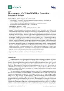
The general arrangement of the neutron sensor is illustrated by figure 1. Our equipment comprises an in-beam equipment (IBE), consisting of the CCD and some support electronics, and an out-of-beam equipment (OBE), providing CCD control, analogue signal processing and a frame-grabber interface. The IBE and OBE are connected by an umbilical cable providing power and timing signals to the IBE from the OBE, and transmitting CCD video output from the IBE to the OBE. The equipment is operated under PC control; frames are captured continuously and stored in portable network graphics 1 (PNG) format. A typical frame rate is 2 s− . We operate our CCD at a 5 MHz pixel frequency. Low-voltage digital signalling (LVDS) is used for the CCD clock transmission. The IBE incorporates LVDS receivers and additional circuits to reconstitute correct CCD clock levels, along with an active load for the CCD and a driver for the video output. Care was taken in laying out the IBE to minimise the neutron fluence received by the support electronics, to minimise the risk of false alarms due to spurious SEE events in those components. The IBE layout took advantage of the tight footprint (approximately 5×12 cm) of the TRIUMF neutron beam, as shown in figure 2. The CCD and support electronics (LVDS receivers, CCD clock drivers, and video amplifier) were mounted on a standard eurocard-size PCB, fully enclosed so as to exclude light. During the trials the IBE package was lowered into the neutron beam from above. The CCD sensor was positioned at the bottom of the IBE board, whereas the support electronics were positioned at the top of the board, as shown, to minimise these components’ exposure to radiation. Only passive components – predominantly decoupling capacitors – were permitted in the region between the CCD and the support electronics. Passive components are generally robust to neutron radiation.
174
This layout also enabled a soak test to be performed in which the IBE was lowered further into the beam, so that the control electronics were irradiated directly. No false alarms attributable to SEEs in the support electronics were observed over a period of 1.5 hours, confirming the robustness of the devices selected to neutron irradiation and permitting IBE layout constraints to be eased for future designs. PC In-beam area
10 m CCD control signals
IBE 5 MHz video
Out-of beam area
OBE
12-bit video Frame grabber Control parameters
Figure 1. Neutron sensor schematic arrangement.
Support electronics
Beam footprint: soak test
Beam footprint: CCD irradiation
CCD
Figure 2. In-beam equipment layout. 4. Example neutron interaction results Figure 3(a) shows an example frame captured during trials at the TRIUMF Neutron Irradiation Facility. Typically, around 1 in 3,000 neutrons is found to cause events exceeding a pixel threshold level of 20 ke− (40 µC.m−2). There are around 300 such events in the frame shown in this figure. Figure 3(b) shows a magnified image of a portion of the same frame, showing several neutron interactions in more detail and showing the improvement achieved with this 9 µm sensor over that possible in earlier work [7], which used a 22 µm sensor. This improved resolution is important not only to permit multiple SEEs in the same image to be resolved, but also to define the spatial extent of neutron-induced charge. This is expected to be important, for example, in predicting MBU rates [8].
175
(a) (b) Figure 3. A typical neutron SEE image: (a) full frame; (b) detail. An example of the type of detailed information available from the sensor is shown in figure 4. Here, a neutron has struck a silicon ion in a pixel near the left of the figure, causing a nuclear reaction the products of which are an aluminium ion and a 4 MeV proton. By chance the proton travels approximately in the plane of the CCD, clearly showing the rate of charge generation along its path (to the right as shown), terminating in a characteristic Bragg peak. This is illustrated further in figure 5, where the x-axis represents distance along the proton path from the point of neutron impact. The proton travels approximately 100 µm; in contrast, the more massive aluminium ion travels a very short distance, generating all of its charge very close to the point of impact. This causes saturation of the pixel signal at this point, leading to blooming along the CCD column, visible in figure 4. Although blooming reduces the resolution of the SEE image along the column, the total charge generated can still be determined. The total charge associated with this event is 0.5 pC, sufficient to cause an upset in many electronic devices.
Figure 4. Example SEE interaction showing a neutron strike releasing a 4 MeV proton.
Figure 5. SEE charge profile along the proton track shown in figure 4.
5. Conclusion The development and application of an imaging neutron sensor, based on a CCD, has been described. The sensor can be used to measure SEE-induced spurious charge profiles in two dimensions at 9 µm resolution. This is of importance in the study of neutron-induced single-event effects in microelectronic devices. Example results have been given; a large data set is being analysed in order to characterise the mechanisms and statistics of SEE phenomena including multiple-bit upsets.
176
Acknowledgements This work was funded by BAE SYSTEMS Air Systems Warton and the UK Department of Trade and Industry as part of the SPAESRANE (Solutions for the Preservation of Aerospace Electronics Systems Reliability in the Atmospheric Neutron Environment) project. References [1] Messenger G C and Ash M S 1997 Single-Event Phenomena (New York: Chapman & Hall) [2] International Electrotechnical Commission 2004 Process Management for Avionics Industry – Standard for the accommodation of Atmospheric Radiation Effects via Single Event Effects within Avionics Electronic Equipment IEC TC107/29/CD (draft) [3] Zeigler J F 1996 Terrestrial Cosmic Rays IBM J. Res. Dev. 40 pp19–39 [4] Dyer C, Truscott P, Sanderson C, Colwell B, Chugg A, Jones R, MacDiarmid I and Johansson K 2000 Cosmic radiation effects on avionics, an increasing hazard in the new millennium? Proc. ICAS 2000 Congress (Harrogate) [5] Blackmore E W, Dodd P E and Shaneyfelt M R 2003 Improved capabilities for proton and neutron irradiations at TRIUMF, IEEE NSREC 2003 Radiation Effects Data Workshop. Available online at http://www.triumf.ca/pif/nsrec2003_paper.pdf [accessed 14 March 2005] [6] Kodak Image Sensor Solutions 2003 Kodak KAF0402E/ME Device Performance Specification. Available online at http://www.kodak.com/global/plugins/acrobat/en/digital/ccd/products/ fullframe/KAF-0402ELongSpec.pdf [accessed 14 March 2005] [7] Chugg A M, Jones R, Moutrie M J and Truscott P R 2004 Analyses of images of neutron interactions and single particle displacement damage in CCD arrays IEEE Trans. Nuc. Sci. NS-51 II 3579–3584 [8] Chugg A M, Moutrie M J and Jones R 2004 Broadening of the variance of the number of upsets in a read-cycle by MBUs NSREC 2004 IEEE Trans. Nuc. Sci. NS-51 II 3701–3707