HARDMEKO 2007 Recent Advancement of Theory and Practice in Hardness Measurement 19-21 November, 2007, Tsukuba, Japan
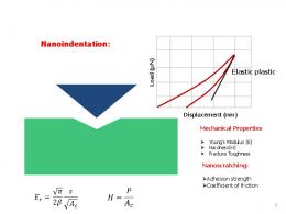
DEVELOPMENT OF A MICRO-MINIATURE NANOINDENTATION INSTRUMENT Zhi Li, Sai Gao, Konrad Herrmann Physikalisch- Technische Bundesanstalt, Braunschweig, Germany Among the various methods for Abstract characterizing the mechanical properties of small volume of materials, nano-indentation testing has gained more and more interests, due to its simple principle, the easy realization and application for various specimen, etc. However, nano-indentation instruments often fail to measure the mechanical properties of materials which demonstrate heavy creep, plasticity, etc. To overcome the disadvantages of nano-indentation instruments, here a new approach to develop the next generation of nano-indentation systems is proposed, in which the well-developed MEMS technique is employed. As one of the key components in the to be developed system, the loading component is now realized by an electrostatic comb-drive actuator, which can generate the required indentation force with high resolution. This microminiature indentation system will feature the advantages of small size, low power consumption, high precision in manufacture, the potential for low cost through batch fabrication, the ability for on-site applications, etc. In this paper the design of the MEMS system is detailed, including the simulation of the mechanical system and the system performance. Keywords: Micro-miniature, nano-indentation, MEMS 1. INTRODUCTION Thin films, coatings and surface treatments are used in many applications requiring special or unique properties. As is well-known, small volumes of materials near and at surfaces often control the performance of the whole specimen. Therefore, how to measure small-volume materials properties in these applications has long been one of the focus within the field of material research, particularly when the thickness of these thin films/layers tends to be thinner and thinner. Compared with those other methods for characterizing the mechanical properties of small volume of materials, nanoindentation testing, in which the test force and the displacement of the indenter are recorded during the indentation process and these data are analyzed to obtain the contact area, and thereby mechanical properties, without having to see the indentations, has gained more and more interests, due to its simple principle, easy realization and application to various specimen. In many cases nanoindentation testing is the only possible method for
probing both the plastic and elastic mechanical properties of thin layers. For the time being, the basic working principles of nanoindentation testing have already been effectively established (see also Ref. [1]-[4]), and related ISO standards on test procedure and data analysis for nanoindentation testing have been developed recently [5]-[6]. Several types of nano-indentation instruments/systems (e.g. [7-10]) are commercially available, which feature, in general, high resolution for generating the indentation force and for measuring the indentation depth, especially when the specimens under test are of hard materials. On the other hand, they also share common shortcomings, such as high costs, difficulties for on-site applications or for applications to test large work pieces, and so on. All these disadvantages strongly restrict the potential widespread application of the current commercially available nano-indentation systems. In the meantime, noting that almost all commonly-used nano-indentation instruments are "soft" force controlled machines, i.e. the indentation force is applied in such a way that small changes in displacement should not change the force significantly, therefore, to our knowledge, nanoindentation instruments often fail to measure the mechanical properties of materials which demonstrate heavy creep, plasticity, etc., since the indentation depth in these cases (under the force control cycles) grows quickly and thereby the applied indentation force cannot be maintained any more. Under consideration that more and more soft materials, such as various biological specimens and organic materials, are now being required to measure their mechanical properties with the nano-indentation method, this disadvantage of the current nano-indentation instruments becomes more and more unacceptable. In order to overcome the above mentioned disadvantages of nano-indentation instruments, it has been more and more demanded to further develop the nano-indenters. Here a new approach to develop the next generation of nano-indentation systems is proposed, in which the well-developed MEMS technique is employed. As one of the key components in the to be developed system, the loading component is now realized by an electrostatic comb-drive actuator, which can generate the required indentation force with high resolution. Similar to other MEMS products/systems, this microminiature indentation system feature the advantages, of small size, low power consumption, high precision in
manufacture, the potential for low cost through batch fabrication, ability for on-site applications, etc. In this paper the design of the MEMS system is presented, including the simulation of the mechanical system and the system performance. 2. PRINCIPLE OF THE MICRO-MINIATURE NANOINDENTATION INSTRUMENT Micro-electro-mechanical systems (MEMS) enable suspended microstructures to be driven precisely for linear or angular motion. Various actuation mechanisms, such as thermal/bimetallic bimorph, electromagnetic, piezoelectric and electrostatic actuation, have been established and applied fundamentally in MEMS-based devices where mechanical actuation is required. Among them electrostatic actuators form the most ubiquitous MEMS family, as summarized in [11], having a force output lying mid-range at 10 6 N~10 3 N and offering relatively large displacements with adequate resolution. The comb-drive-type electrostatic microactuator might be one of the most important electrostatic MEMS actuators, which has in general a large number of fine interdigitated fingers to generate the actuated force. 2.1. Principle of the lateral comb-drive actuator As shown in Fig.1, the electrostatic comb-drive actuator consists of two interdigitated finger structures, in which one is fixed and the other one is movable. The force generated by each comb-pair during electrical actuation is [12]: h 2 V d in which, 0 8.85 10 fe
(1)
0
12
Fm 1 is the permittivity constant, h is
the height of the comb and d is the lateral gap between the movable and the fixed combs. Cp
movable finger fixed finger
x0
d
Findent
N
0
Fe
h 2 V d
Findent
k z.
(4)
As a result, an indentation instrument with lateral combdrive actuator can easily realise the true force-controlled indentation procedure, without any necessity to care about the actual mechanical properties of the material under test. With typical Bonding-DRIE (deep reactive ion etching) technology [13] in the Chemnitz University of Technology (Germany), the parameters in Fig. 1 can be: h = 50 µm, d = 3 µm. 2.2.Spring design of the comb-drive actuator As defined in equation (4), the actual indentation force is determined not only by the driving voltage and the structure parameters of the force actuator, but also by the spring constant of the actuator, i.e. Findent
2N
0
h V d
2
1/ 2
V2
k2
z2
.
(5)
In order to obtain a resolution of the indentation force of ca. 50 nN, suppose that the displacement of the movable electrodes of the actuator can be tracked with nanometric resolution, the spring constant of the miniature indentation instrument should be less than 50 N/m. In this paper, two types of supporting springs are investigated: one is the single beam spring [as shown in Fig. 2(a) ], and the other is of the folded beam structure [as depicted in Fig. 2(b)].
h
x
C
(2) in which m is the mass of the indenter, z is the indentation depth, Findent is the reaction force between the indenter and the material under test, k is the equivalent spring constant of the indentation system, and Fe is the actual electrostatic force of the force actuator with N pairs of comb-fingers, i.e. Fe = N fe . Compared with the traditional parallel-plate capacitive transducer, it can be seen from equation (2) that since Fe is now independent of the variation of the actual indentation depth h, the real indentation force can be easily determined by (3) Findent Fe (m z c z k z ) . In the case of quasi-static indentation testing, we get m z c z k z
t
Fig. 1. Principle of the lateral comb-drive actuator
One of key advantages of the lateral comb-drive structure is that the electrostatic force generated by the microstructure is independent of the displacement of the movable electrodes (plates). Consequently, when an indenter is driven by the electrostatic actuator to make an indent on the top surface of a specimen, the typical kinetics of the indentation procedure can be represented as follows:
Fig. 2(a) Single-beam supporting beam and its typical stress distribution under condition of bending.
as possible the adhesive between the sphere and the holder by means of the siphon effect.
Tip container
Tip 1 Dia. = 50 µm Tip 2 Dia. = 100 µm Fig. 2(b) Folded-beam spring and its typical stress distribution under condition of bending.
It can be seen from Fig. 2 that under the condition of the same (in-plane) spring constant, a multi-folded spring structure helps a lot to reduce the inner stress within the spring, and therefore can effectively increase the reliability and life time of the micro-device. Finally, the relationship between the electrodes displacement and the corresponding spring force is illustrated in Fig. 3, which indicates excellent linearity within the required displacement range.
Fig. 4. Schematic diagram of the tip container for the miniature indentation instrument
(a) Deformation of the tip container
Fig. 3 FEA simulation to the multi-folded spring used in the miniature indentation instrument.
2.3. Tip container design It can be predicted that to fabricate the typical indenter tip as defined in [6]-[7] with integrated MEMS technique would be very difficult. Therefore, in this paper we prefer to mount a commercial indenter (e.g. a perfect ruby sphere) to the micro-device with post-assembly technique. A creful design of the tip container is essential to maintain the measurement accuracy of the micro-device. Fig. 4 demonstrates the schematic of the tip container for a sphere with a diameter of 50 ~ 100 µm. The ball-shaped indenter is expected to be connected to the container with an optical adhesive. In the middle of the V-shaped tip container, a rectangle groove is predefined, with the aim to pull as more
(b) Inner stress distribution of the tip container Fig. 5 Deformation and stress distribution
of tip container under indentation testing
With FEA simulation, the mechanical performance of the tip container was investigated. Under the condition of a sphere of 100 µm diameter being mounted on the container, when a 0.5 mN indentation force is applied on the specimen, the deformation and the stress distribution of the tip are shown in Fig. 5, which indicate that the maximum deformation is about 2.3 nm, and the maximum stress is 2.5 MPa. 2.4 System design of the miniature indentation instrument The miniature indentation instrument is developed with the aim mainly to measure the mechanical properties of those layered materials as metal, plastic and organic material, etc. As shown in Fig. 6, with a sphere of 100 µm diameter, the maximum indentation force of about 0.5 mN would be sufficient to perform nanoindentation tests on a material like aluminium.
Fig. 6. Indentation curve with a spherical indenter of 100µm diameter on bulk aluminium (simulation result). Therefore the miniature indentation instrument is designed to have 2000 finger pairs in the comb-drive, generating 0.74 mN at the zero-position and 0.6 mN (net indentation force) at the axial displacement of 5 µm with a driving voltage of 50V, respectively. The overall structure of the final micro-device is shown in Fig. 7, which is fabricated with typical DRIE technique and silicon-silicon bonding.
3. CONCLUSIONS In order to overcome the disadvantages of the currently available nanoindentation instruments, a miniature indentation instrument is developed, which is based on a lateral comb-drive actuator, and features accurate indentation force in spite of the mechanical properties of the materials under test. The overall dimension of the miniature indentation instrument is about 4.5 mm × 3.2 mm, which is much smaller than the conventional nanoindentation instruments, and therefore enables that the miniature instrument can be applied for on-site measurements. REFERENCES [1] M.F. Doerner, W.D. Nix, "A method for interpreting the data from depth sensing indentation instruments", J. Mater. Res., vol. 1, pp. 601-609, 1986 [2] W.C. Oliver, G.M. Pharr. An improved technique for determining hardness and elastic modulus using load and displacement sensing indentation experiment, J. Mater. Res. vol. 7, pp. 15641583, 1992. [3] Pharr, G.M; Bolshakov, A. "Understanding nanoindentation unloading curves", Journal of Materials Research, vol. 17 no. 10, pp. 2660-71, 2002. [4] S. Rajagopalan, R. Vaidyanathan, Nano- and microscale mechanical characterization using instrumented indentation. JOM, vol. 54, no. 9, pp.45-48+60, 2002. [5] ISO 14577-1 (2002): Metallic materials - Instrumented indentation test for hardness and materials parameters - Part 1: Test method. [6] ISO 14577-2 (2002): Metallic Materials - Instrumented indentation test for hardness and materials parameters Part 2:Verification and calibration of testing machines [7] MTS Systems Corporation, 1001 Larson Drive Oak Ridge, TN 37830-8014 USA [8] Hysitron Inc., 5251 West 73rd Street, Minneapolis, MN, 55439 USA [9] Micro Materials Ltd., Unit 3, The Byre, Wrexham Technology Park, Wrexham LL137YP, United Kingdom. [10] CSM Instruments, Jaguet-Droz 1, P.O. Box 41, CH-2007, Neuchatel Switzerland. [11] D.J. Bell, T.J. Lu, N.A. Fleck, S.M. Spearing, MEMS actuators and sensors: observations on their performance and selection for purpose, J. Micromech. Microeng. 15, pp. S153S164, 2005. [12] W. C. Tang, C. H. Nguyen, and R. T. Howe, Laterally driven polysilicon resonant microstructures, Sensors Actuators A, 20, pp. 2532, 1989. [13] K. Hiller, M. Kuechler, et al. Bonding and Deep RIE - a powerful combination for high aspect ratio sensors and actuators, Proc. of SPIE (Micromachining and microfabrication process technology X) vol. 5715, pp. 80-91, 2005. Author: Dr. Zhi Li, PTB 5.12,
[email protected] Dr. Sai Gao, PTB 5.12,
[email protected] Dr. Konrad Herrmann, PTB 5.12,
[email protected], tel: +49-531-5925140, fax: +49-531-5925105.
Fig. 7. 3-D view of the developed miniature nanoindentation instrument, which uses a lateral comb-drive actuator to generate the indentation force.
Acknowledgement: This paper is supported by the Deutsche Forschungsgemeinschaft (DFG) under the project number HE2235/5-1