achieved using novel current division network (CDN). The proposed DCBOTA operates under low supply voltage of. ±1.5V. Application of the DCBOTA is ...
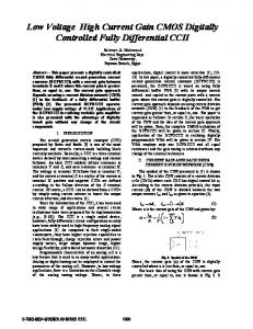
Digitally Controlled CMOS Balanced Output Transconductor Based on Novel Current-Division Network and Its Applications Mohammed A. Hashiesh1, Soliman A. Mahmoud1, and Ahmed M. Soliman2 1. Electrical Engineering Dept., Cairo University, Fayoum Branch, Egypt. 2. Electronics and Communication Eng. Dept., Cairo University, Cairo, Egypt. Abstract: In this paper, a novel digitally controlled CMOS balanced output transconductor (DCBOTA) is proposed. The digital control of the transconductance of this DCBOTA is achieved using novel current division network (CDN). The proposed DCBOTA operates under low supply voltage of ±1.5V. Application of the DCBOTA is realizing variable gain amplifier VGA and second order active filter. PSPICE simulation confirms the performance of the proposed blocks and its applications. I. INTRODUCTION The programmable balanced output transconductor (BOTA) is a useful building block for continuous-time analog signal processing. Based on the BOTA circuit, balanced output integrators, MOS-C filters with balanced outputs and active realization of passive filters with minimum number of BOTA can be built [1,2]. In low voltage applications, there is a limitation on the allowable range of the analog tuning voltage. Hence, in these applications, digital control is more attractive [3]. Another example utilizing digital control is the interface with the digital signal processing unit (DSP) in the modern digital systems. For example the variable gain amplifier (VGA) is used in many applications in order to maximize the dynamic range of the overall system by varying the gain of the VGA. Wireless communication is an example of such systems [4]. In modern wireless systems, all of the baseband signal processing is implemented digitally by a digital signal processor. Hence, a primary requirement of the VGA is to be digitally controlled [5]. In this paper a novel digitally controlled CMOS balanced output transconductor (DCBOTA) is presented. The digital control of the DCBOTA is achieved using novel current division network (CDN) that will be discussed in section III. The traditional approach to implement the CDN is to use the well-known resistive R-2R ladder circuit. For proper operation, all the resistance in the ladder must be matched. This may be very difficult to achieve in practice especially when number of bits increases. Another drawback is that the output resistance of this CDN is small. This means that the output nodes IO1 or IO2 should be at virtual ground voltages. This prevents the use of this circuit in the applications where the input resistance of the stage next to the CDN is finite. In the DCBOTA, the output current of the CDN is mirrored using MOS transistor which has finite input resistance. Hence, a resistive ladder CDN cannot be used in this application. A better approach to implement the CDN is to use of MOS ladder circuit [6]. In spite of the advantages of this
circuit over its resistor-based counterpart, its structure is similar to the classical resistor based R-2R ladder CDN and still suffers from the drawbacks of it such as finite output resistance, the need of matching all the transistors in the circuit, and the requirement of matched output node voltages of nodes IO1 and IO2. The CDN presented in [3] uses differential-pair current division cell (CDC) technique to divide the input current of the CDC into two equal divisions if the gates of the two MOS transistors constructing the differential pair are kept under the same voltage level. For proper operation, the n-bits CDN requires (n+1) biasing voltages to be connected to the gates of the differential pairs of the n-CDCs. To generate those biasing voltages, a very complex design is required. The number of control bits is limited by those biasing voltages which are limited by the power supply range. As in the differential-based CDN, the proposed CDN has very high output resistance since the output currents are drown from the drain of the transistors (as will be discussed later). Hence, no need for virtual ground nodes. Consequently, the aspect ratio of the transistors can be chosen arbitrary to achieve the required current level without putting stringent requirement on the stage next to the CDN. Besides, only the transistors inside each CDC are required to be matched rather than matching all the transistor in the entire CDN. Hence, the matching-requirements are relaxed. Since the transistor are assumed to operate in the saturation region, higher current drive capability is expected than in the case of the MOS ladder for the same aspect ratios of transistors. Moreover, the proposed CDN has no limitation on the number of the control bits as in the case of the differential-based CDN. And no need to external biasing voltages. II. THE PROPOSED DCBOTA The CMOS realization of the proposed DCBOTA circuit is shown in Fig. 1(b). It consists of a basic four matched-transistors M1-M4 drive two similar CDNs. The output currents of the two CDNs are transferred to output nodes by the rest of the circuit M5-M14 to get the two balanced output currents of the DCBOTA. As will be discussed in the following section, the value of the input current to the CDN is divided between two complementary output currents depending on the digitally controlled parameter Į (IO1=ĮII, and IO2=(1-Į)II). The two current division blocks (CDN1 and CDN2) in Fig. 1(b) are controlled by the same control word. Hence, the output current of the DCBOTA can be driven as follows:
The matched transistors M1-M4 are the basic transistors, and their gate voltages are the input voltages to the transconductor. All transistors are assumed to be operating in saturation region with their sources connected to their substrate/bulk. The MOS drain current in the saturation region is given by: K (1) ID (VGS � VT ) 2 2 Where K=µnCox(W/L); (W/L) is the transistor aspect ratio, µn is the electron mobility, Cox is the gate oxide capacitance per unit area, and VT is the threshold voltage (assumed the same for all MOS transistors). From Fig. 1(b), (2) I OA I1 � I 4 (3) I OB I 2 � I 3 The first current-division of CDN1 and CDN2 is ĮIOA and ĮIOB respectively. The remaining transistors M5-M14 perform current transfer for those two currents to the output port of the transconductor, hence, the output current of the transconductor Io is given by: (4) I O D ( I OA � I OB ) Using equations (1)-(4), the transconductor output current is given by: (5) I O DK (VC � VSS )(V1 � V2 ) Therefore, the proposed DCBOTA circuit shown in Fig. 1 operates as a digitally controlled balanced output transconductor with programmable transconductance G which is controlled by the digitally controlled parameter Į and is given by: (6) G DK (VC � VSS )
I O1i
I Ii 2 I Ii ai 2 I Ii 2
ai
I O 2i
I O 3i
(7) (8) (9)
Where ai is the digital control bit of this cell. As shown from Fig. 2, IO3i of the CDCi is used as the input current of the next stage II(i-1) and IO30 has inverted direction, as will be discussed later, and is added to IO2. Therefore, the two output currents of the CDN are given by: i n �1 1 § i n�1 i · (10) I O1 ¦ I O1i ¨ ¦ 2 ai ¸ I I 2n © i 0 i 0 ¹ i n �1
IO2
I O 30 �
¦I i 0
O 2i
1 § i n�1 i · ¨1 � ¦ 2 a i ¸ I I 2n © i 0 ¹
(11)
I O1 1 § i n �1 i · (12) ¨ ¦ 2 ai ¸ II 2n © i 0 ¹ Hence, the current gain of the proposed CDN is digitally controlled. D
Fig. 2: Proposed CDN Block Diagram
Fig. 3: Proposed CDC (a) Symbol (b) CMOS Realization
Fig. 1: Proposed DCBOTA (a) Symbol (b) CMOS Realization
Note that the tuning of the DCBOTA is achieved using the digitally controlled parameter Į where Į1; i.e. the maximum transconductance value is achieved at Į=1 and is equal to K(VC-VSS) where VC and VSS are DC control voltage and the negative supply voltage respectively. The operation of the CDN block is described in the following section. III. THE PROPOSED CDN The block diagram of the proposed CDN is shown in Fig. 2. It consists of n current division cells (CDCs). According to the current division principle, each CDC of this network has three output currents. The output currents of the current division cell number i CDCi are IO1i, IO2i, and IO3i whose relations to the input current of this cell (IIi) are expressed as follow:
The proposed CDC is shown in Fig. 3. For the matched transistors MA1-MA4, the input current of the CDCi (IIi) is divided between MA1 and MA2 then this value is transferred to both MA3 and MA4 by the current mirror effect. Only one transistor of MA5 or MA6 is on at a time due the value the digital control bit ai. Hence, the current of IIi/2 which flowing through MA3 is either switched to IO1i or IO2i as equations (7) and (8) indicate. The current flowing through MA4 ,which also equal to IIi/2, is transferred to IO3i through MA7 and MA8 as stated in equation (9). For the last stage CDC0, no need to MA7 and MA8 and the current IO30 is simply equal to the current of MA4. The proposed DCBOTA circuit has been simulated using PSPICE simulation with 0.5µm CMOS parameters (level3). The power supply voltages VDD and VSS are balanced (1.5V and -1.5V) respectively. The aspect ratios of the transistor are given in Table 1 and n = 8 bits. The DC control voltage (VC) is –1.1 V. The two balanced output currents of the DCBOTA is shown in Fig. 4 when driving RL+=RL-=8Kȍ and the differential input voltage is swept from –1 to 1V for different values of the digitally controlled
parameter Į ranging from 0 to 1 in 0.125 step. Fig. 5 shows the frequency response of the output current when RL+=RL=8Kȍ and Į = 1 from which it is seen that the bandwidth is approximately equal to 21 MHz Table 1: Aspect Ratios of The Proposed DCBOTA Transistor Aspect Ratio [µm/µm]
M1, M2, M3, M4. M5, M6, M7, M8, M9, M10. M11, M12, M13, M14. MA1, MA2, MA3, MA4, MA5, MA6, MA7
22/6 80/2 160/2 100/1
Fig. 4: DC Transfer Characteristics of The Proposed DCBOTA
Fig. 5: Frequency Response of The Output Current of The Proposed DCBOTA
IV. DIGITALLY PROGRAMMABLE FULLY DIFFERENTIAL VGA Variable gain amplifiers (VGA) are employed in many applications in order to maximize the dynamic range of the overall system. For example; in any portable communication system, the VGA is employed in feedback loop to realize an automatic gain control loop (AGC)[7]. Receiver portability implies that the receiver may be very close to the transmitter and thus receiving strong signal, or far away receiving weak signal. The function of the AGC loop is to automatically adjust the gain of the receiver path so that the signal processed by the base band circuitry appears to be of constant level regardless of the actual signal size received at the antenna. In modern wireless systems, all of the baseband signal processing is implemented digitally by a digital signal processor. Hence, a primary requirement of the VGA is to be digitally controlled [5]. The digitally-controlled fully-differential VGA can be implemented using DCBOTA as shown in Fig. 6. For Fig. 6(a), The VGA circuit consists of DCBOTA Transconductor driving load resistance RL. The DCBOTA has transconductance G given by equation (6). Thus, the fully differential output voltage (VO1-VO2) can be driven as follows: (13) (VO1 � VO 2 ) 2GR L (V1 � V 2 )
Where G is controlled by Į, Į is the digital control parameter given by equation (12). Hence the number of the control bits is 8 bits, and from equation (12), if the value of 2GRL/Į is designed to be equal 28, The above configuration of the VGA can be operated with dB-linear gain if Į has only one bit of the 8 control bits activated at a time as shown in Table 2. Thus could be obtained using simple 3X8 decoder to reduce the required control word to only 3 bits. The minimum gain is 0 dB and is obtained when the least significant bit is active. The maximum gain is 42 dB when the most significant bit is active. Hence, the gain step is 6 dB that appear to be quit large. To realize dB-linear VGA with wide control range and fine step, two DCBOTAs are cascaded as shown in Fig. 6(b). DCBOTA2 and its load RL2 are designed as in the previous configuration to operate with 6 dB coarse step controlled by Į2 while DCBOTA1 and RL1 are designed to operate with the required fine step with the appropriate decoder, the VGA is thus operating in a fine and coarse arrangement. The differential gain of the proposed VGA in Fig. 6(a) is sown in Fig. 7 in dBs versus the differential input voltage when the gain is scanned from 0 dB to 30 dB with gain step of 6 dB, where the DCBOTA is designed as in Table 1 and RL=1.25Mȍ.
Fig. 6: Proposed VGA (a) First Configuration (b) Second Configuration
Fig. 7: dB Gain of The Proposed VGA at Gain Step = 6 dB
V. DIGITALLY PROGRAMMABLE FILTER The active filter presented in [2] can be implemented using DCBOTA to handle the advantages of the digital control and simply interface the DSP units in the modern digital systems. Fig. 8 represents this filter circuit which includes four DCBOTAs and two grounded capacitors and realizes second-order lowpass, bandpass, allpass and notch responses. The lowpass and bandpass exist in the voltage and current modes; however, the allpass and notch outputs exist only in current mode and obtained by combining IBP and Ii (Ii is the output current of the transconductor G3). By direct analysis, the following transfer functions are obtained:
VLP Vi VBP Vi Where, D( S )
G1G3 C1C2 I LP , D( S ) Vi SG3 C1 I BP , D(S ) Vi
�
S2 �
G1G2G3 C1C2 (14) D( S ) SG1G3 C1 (15) D(S ) �
GG G S� 1 2 C1 C1C 2
(16)
From the above equation, the wo and Q of the filter are given by: G1G2 1 G1G2 C1 (17) wo , Q C1C 2 G C2
Table 2: Digital Control Word For The Proposed dB-Linear VGA Digital Control Word Gain
a7 0 0 0 0 0 0 0 1
a6 0 0 0 0 0 0 1 0
a5 0 0 0 0 0 1 0 0
a4 0 0 0 0 1 0 0 0
a3 0 0 0 1 0 0 0 0
a2 0 0 1 0 0 0 0 0
a1 0 1 0 0 0 0 0 0
a0 1 0 0 0 0 0 0 0
dB
0 6 12 18 24 30 36 42
VI. CONCLUSION In this paper, a novel digitally controlled CMOS balanced output transconductor DCBOTA has been proposed. Novel current division network CDN has been used to provide the digital control of the transconductance of this transconductor that simply is a four-transistor cell. Application of the DCBOTA is realizing dB-linear variable gain amplifier VGA and second order active filter. The proposed DCBOTA and its applications have been confirmed using PSPICE simulation. Fig. 8: DCBOTA-C Active Filter
The circuit of Fig. 8 has been simulated using PSPICE simulation with C1=C2=7pF, and G1=G2=G3=20G=ĮK(VCVSS) µA/V-1 to obtain bandpass filter with Q=20, and digitally tunable fo. The frequency response of that filter is shown Fig. 9 for different values of the digital control parameter Į. Fig. 10 shows the simulation results for the same circuit with C1=C2=7pF, and G1=G2=G3=0.707G =ĮK(VC-VSS) µA/V-1 to obtain a maximally flat low pass response for a DC gain of 1 and with digitally tunable fo for different values of the digital control parameter Į.
Fig. 9: The Magnitude Response of the Voltage-Mode Bandpass Output
Fig. 10: The Magnitude Response of the Voltage-Mode Lowpass Output
REFERENCES [1] S. A. Mahmoud, and A. M. Soliman, ”A CMOS Programmable Balanced Output Transconductor For Analog Signal Processing,” Int. J. Electron. Commun., vol. 82, pp. 605-620, 1997. [2] S. A. Mahmoud, and A. M. Soliman, ”CMOS Balanced Output Transconductor and applications for analog VLSI,” Microelectronics journal, vol. 30, pp. 29-39, 1999. [3] A. A. El-Adawy, A. M. Soliman, and H. O. Elwan, “Low Voltage Digitally Controlled CMOS Current Conveyor,” Int. J. Electron. Commun., vol. 56, pp. 137-144, 2002. [4] S. A. Mahmoud, and I. A. Awad, ”Digitally Controlled Balanced Output Transconductor and Applications,” 15th International Conference On Microelectronics, ICM03, Cairo, Egypt, pp.211-214, Dec.9-11, 2003. [5] H. O. Elwan, and M. Ismail, “Digitally Programmable Decible-Linear CMOS VGA For Low Power Mixed Signal Applications,” IEEE Trans. Circuits Syst. II, vol. 47, pp. 388-398, 2000. [6] K. Bult, and G. J. G. M. Geelen, “An Inherently Linear and Compact MOST-Only Current Division Technique,” IEEE J. Solid-State Circuits, vol. 27, pp. 1730-1735, 1992. [7] G. Sahota, and C. Persico, “High Dynamic Range Variable-Gain Amplifier for CDMA Wireless Applications, ” in ISSCC97, pp. 374-375, 1997.