Due to the stringent page limitation, the proof is omitted. However, we can say .... for the exhaustive verification of the Collatz conjecture,â in Proc. of. International ...
A Flexible-Length-Arithmetic Processor Using Embedded DSP Slices and Block RAMs in FPGAs Md. Nazrul Islam Mondal, Kohan Sai, Koji Nakano, and Yasuaki Ito Department of Information Engineering, Hiroshima University 1-4-1 Kagamiyama, Higashi-Hiroshima, 739-8527, Japan
Abstract—Some applications such as RSA encryption/decryption needs integer arithmetic operations with many bits. However, such operations cannot be performed directly by conventional CPUs, because their instruction supports integers with fixed bits, say, 64 bits. Since the CPUs need to repeat arithmetic operations to numbers with fixed bits, they have considerably overhead to execute applications involving integer arithmetic with many bits. On the other hand, we can implement hardware algorithms for such applications in the FPGAs for further acceleration. However, the implementation of hardware algorithm is usually very complicated and debugging of hardware is too hard. The main contribution of this paper is to present an intermediate approach of software and hardware using FPGAs. More specifically, we present a processor based on FDFM (Few DSP slices and Few Memory blocks) approach that supports arithmetic operations with flexibly many bits, and implement it in the FPGA. Arithmetic instructions of our processor architecture include addition, subtraction, and multiplication for numbers with variable size longer than 64 bits. To show the potentiality of our processor, we have implemented 2048-bit RSA encryption/decryption by software written by machine instructions. The resulting processor uses only one DSP48E1 slices and four Block RAMs (BRAMs), and RSA encryption software on it runs in 635.65ms. It has been shown that the direct hardware implementation of RSA encryption runs in 277.26ms. Although our intermediate approach is slower, it has several advantages. Since the algorithm is written by software, the development and the debugging are easy. Also, it is more flexible and scalable. Index Terms—Multiple-length-arithmetic, Montgomery Modular Multiplication, FPGA, DSP Slices, Block RAMs.
I. I NTRODUCTION An FPGA is a programmable logic device designed to be configured by the customer or designer by HDL (Hardware Description Language) after manufacturing. An FPGA chip maintains relative lower price and programmable features [1], [2], [3], hence, it is widely used recently. We refer the readers to see some circuit implementations in FPGAs [4], [5], [6], [7], [8], [9], [10], [11], [12] to accelerate computation. In particular, since, FPGAs can implement hundreds of circuits that work in parallel, they are used to accelerate useful computations. Applications require arithmetic operations on integer numbers which exceed the range of processing by a CPU directly is called Multiple Double Length Numbers or Multiple Precision Numbers and hence, computation of these numbers is called Multiple-Length-Arithmetic. More specifically, application involving integer arithmetic operations for multiple-length numbers with size longer than 64 bits cannot be performed directly
by conventional 64-bit CPUs, because their instruction supports integers with fixed 64 bits. To execute such application, CPUs need to repeat arithmetic operations for those numbers with fixed 64 bits which increase the execution overhead. Alternatively, hardware algorithms for such applications can be implemented in FPGAs to speed up computations. However, the implementation of hardware algorithm is usually very complicated and debugging of hardware is too hard. Since, low level of instructions, represented by 0’s and 1’s is an almost impossible to understand even by an expert, the debugging of an algorithm at this level is very hard. Moreover, to implement hardware algorithm, written by hardware language such as Verilog HDL, users should have sufficient knowledge of hardware such as registers which makes it complicated to the non-expert or to the beginners. The instructions in assembly language are written by alphanumeric symbols instead of 0’s and 1’s in low level that is an almost similar to the high level language, written by English which makes the instructions as well as algorithms easy to read, modify and debugging by the non-expert or by the beginners. The main contribution of this paper is to present an intermediate approach of software and hardware using FPGAs (Field Programmable Gate Arrays) to support arithmetic operations for numbers with flexibly many bits such that the development and debugging of it become easier. More specifically, we propose a flexible-length-arithmetic processor based on FDFM approach that supports applications involving arithmetic operations for numbers with variable size longer than 64 bits and these applications, written by software become easier for debugging and further development. For the reader’s benefit, this paper precisely describes our main contributions as follows: • We propose a flexible-length arithmetic processor based on FDFM approach for computing of integer numbers with flexibly many bits, even longer than 2048-bit by a single machine instruction. • We present an intermediate approach of software and hardware to write the algorithm which makes the debugging and further development easy. • Our designed processor provides flexibility so that it can be used for computing of integer numbers with flexibly many bit such as 64-bit, 128-bit, even longer than 2048bit without further modification. Since, our designed processor based on FDFM approach, the key idea of the FDFM approach is to use few DSP slices
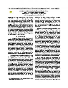
and few block RAMs to perform routine computations which can be treated alternatively as a resource efficient approach. Let us explain briefly the FDFM approach using a simple example. Figure 1 (1) illustrates a hardware algorithm to compute the output of FIR (Finite Impulse Response) yi = a0 ·xi +a1 ·xi−1 +a2 ·xi−2 +a3 ·xi−3 . A conventional approach implementing the FIR is to use four DSP slices as illustrated in Figure 1 (2)[13]. In this conventional approach, the number of DPS blocks must be the same as that of multipliers in the hardware algorithm. However, FDFM approach uses one or few DSP slices and one or few block RAMs to implement the FIR. The Figure 1 (3) shows the FDFM approach using one DSP slice and one block RAM to implement the same mentioned above. Note that, the coefficients a0 , a1 , . . . are stored in the block RAM. xi ×
×
×
by parallel computation.
RAM Main Circuit DSP
(1) Minimum implementation
RAM
RAM
RAM
RAM
RAM
DSP
DSP
DSP
DSP
DSP
(2) Parallel implementation
× Fig. 2.
+
+
+
yi
(1) FIR
xi
DSP
DSP
DSP
DSP
yi
(2) Conventional approach
xi
RAM
yi
DSP (3) FDFM approach
Fig. 1.
FDFM approach over conventional one for FIR
For readers, we also refer to the papers [14], [15], [16], [17] in which they can find details about FDFM approach and conventional approach. Let us describe the two important advantages of the FDFM approach are as follows: 1.
Even if the large main circuit occupies the most of hardware resources in the FPGA, we can implement a necessary hardware algorithm in the FPGA using remaining few hardware resources as illustrated in Figure 2 (1).
2.
Also, if enough hardware resources are available, we can implement multiple FDFM processor cores that work in parallel (Figure 2 (2)). The resulting hardware implementation has maximum throughput
Two advantages of FDFM approach
Because of the above mentioned advantages of the FDFM approach, we design flexible-length-arithmetic processor based on FDFM approach. More precisely, our proposed processor supports minimum implementation in Figure 2 (1). However, if enough hardware resources are available in FPGA, it can be used to work in parallel (Figure 2 (2)) to maximize throughput. Note that, our designed flexible-length-arithmetic processor using FPGA based on FDFM approach can perform arithmetic operations for numbers with variable size longer than 64 bits by a single command or instruction whereas today’s PCs of 64 bits must require complicated arithmetic algorithm with many commands to compute these. The most common FPGA architecture consists of an array of logic blocks, I/O pads, Block RAMs and routing channels. Furthermore, embedded DSP blocks which is integrated into an FPGA that makes a higher performance and a broader application. Figure 3 illustrates the Virtex-6 FPGA developed by Xilinx. The CLB (Configurable Logic Blocks) in Virtex-6 consists of 2 sub-logic blocks called slice. Using LUTs (Look Up Tables) and Flip-Flops in the slices, various combinatorial circuits and sequential circuits can be implemented. The Virtex-6 FPGAs also has DSP48E1 slices equipped with a multiplier, adders, and logic operators, etc. More specifically, as illustrated in Figure 4, the DSP48E1 slice has a two input multiplier followed by multiplexers and a three-input adder/subtractor/accumulator. The DSP48E1 multiplier can perform multiplication of the 18-bit and the 25-bit 2’s complement numbers and produces one 48-bit 2’s complement production. Programmable pipelining of input operands, intermediate products, and accumulator outputs enhances throughput and improves the frequency. The DSP48E1 also has pipeline registers between operators to reduce the delay. The block RAM in the Virtex-6 FPGA is an embedded memory supporting synchronized read and write operations.
�
� � � � � � �� �� �� �� ��
�� ���� ���� �� �� �� �� ��
����
�� �� � � � � � � � � �
Fig. 3.
���� � � � � ����
�� �� �� ��
�� ����
��
�� �� ��
� � � � � � � � � � � �
Internal Configuration of Virtex-6 FPGA
� ×
����� �����
�
� �
�
�
ware written by machine instructions and compare it with direct hardware implementation of 2048-bit RSA encryption/decryption [15], maximized making use of DSP blocks in FPGA. Direct hardware implementation of 2048-bit RSA encryption/decryption module runs in 447.027MHz using 123940864 clock cycles, that is, in 277.26ms. A multiplier in the DSP block works in more than 90 percent over all the clock cycles. Thus, it has minimum overhead. Also, it uses one DSP48E1, one BRAM and few (170) logic blocks (slices). Therefore, this is an optimal implementation. On the other hand, our intermediate approach using our designed processor for implementing 2048-bit RSA encryption/decryption by software uses one DSP48E1, four BRAMs and few (170) logic blocks (slices) that runs in 635.65ms. Although, our intermediate approach is slower, it has several advantages. Since application algorithm is written by software, the development and debugging even by a non-expert are easy. Also, it is more flexible and scalable. We summarize several significant points of our results as follows: •
�� � ����� •
Fig. 4.
Architecture of DSP48E1
In Virtex-6 FPGA, it can be configured as a 36k-bit dual-port block RAMs, FIFOs, or two 18k-bit dual-port RAMs. In our architecture, it is used as a 2k x 18-bit dual-port RAM. We are mainly thinking the following scenario for designing a flexible-length-arithmetic processor: 1) Our aim is mainly to emphasis the beginners or nonexpert users. Since our processor is designed to be implemented for computing numbers even longer than 2048-bit by a single machine instruction, not by hardware language, they can understand or change or modify it easily. More specifically, since the application algorithm is written by software, the development and debugging are easy to them. 2) Our designed processor can be used for integer arithmetic operations on numbers with variable size longer than 64 bits without further modifications. 3) We exploit the feature of embedded DSP (DSP48E1) block in FPGA for processing flexible-length numbers. Because of this feature, we process each 17-bit block of these numbers rather than single bit to speed up computations. To the best of our knowledge, there is no related work so far. However, we have shown the potentiality of our designed flexible-length processor. For this purpose, we have implemented 2048-bit RSA encryption/decryption by soft-
•
•
•
A flexible-length-arithmetic processor is proposed for the applications which require arithmetic operations for numbers longer than 64 bits. Even, numbers longer than 2048 bits or higher can be computed by our designed processor without any modification. We say that our proposed processor is flexible in a sense that it can support arithmetic operations for numbers with flexibly many bits or numbers with variable size longer than 64 bits. We propose an intermediate approach of software and hardware to implement above mentioned applications which makes it easy for debugging and further development by the non-experts or by the beginners. We have shown the potentiality of our designed processor through the implementation of 2048-bit RSA encryption/decryption by software. The resulting processor uses one DSP48E1, four BRAMs and few (170) logic blocks (slices) and RSA encryption software runs in 635.65ms. We compare our results with the results of 2048-bit RSA encryption/decryption optimal implementation [15] by HDL. This optimal implementation requires one DSP48E1, one BRAM and few (180) logic blocks (slices) and runs it in 277.265ms. Although our approach is slower, however, it has several advantages. Since, the application algorithm is written by software, the development and debugging are easy. Also, it is an almost scalable based on experimental results. Further, we compare the results of the execution time for 64-bit, 128-bit, 256-bit, 512-bit and 1024-bit RSA encryption/decryption as illustrated in Table IV. Experimental results show that the execution time ratio of our work over optimal one is decreasing with increasing bit length which indicates that proposed processor architecture will be more efficient for a bit length higher than 2048-bit.
�������
���� ,-�. �/��� �� � 7> > = < 7; 2 63 : 63 8679 5 4 3 2 1
@ ?CAB F ?DE
� � �
�����
� � � �'!&%"#$ ���&�!"#$
� � ���%!"#$ ����!"#$
0 GHIJKLMNLOP ��� � ��
���
Fig. 5.
� �
() (*
� 0
(+) (+*
��������� � � ������ �� �� � � ��
��� Data of 1024-bit Length is Stored in Memory (BRAM)
The rest of this paper is organized as follows: Section II briefly describes the Multiple-length-arithmetic operation. In Section III, we describe our proposed architecture. The RSA cryptography as an application is described briefly in Section IV. Section V describes experimental results and discussions. Finally Section VI concludes this work.
Zero Flag Carry Flag
A B
DSP
d1
q1
Temporary RAM Adder
d2
q2
Output1
Output2
addr1
II. M ULTIPLE -L ENGTH -A RITHMETIC O PERATION The main purpose of this section is to describe MultipleLength-Arithmetic operations. Suppose that A and B are two multiple-length numbers of 1024 bits each. We partition these numbers into several blocks of 17 bits. First, we see that how a multiple-length number of 1024 bits is stored in data memory. Figure 5(a) shows a data memory (BRAM). Every 17-bit block data together with 1-bit flag represents a bit-block of 18 bits and MSB (Most Significant Bit) of each bit-block is known as flag which set to 1 indicates the end of each stored multiplelength data into the data memory as shown in Figure 5(b). In this figure, multiple-length data A of 1024 bits is divided into 61 numbers of 17 bits block such as a0 , a1 , . . ., a60 , a61 . Every 17 bits block of multiple-length data, A together with 1-bit flag is stored in different memory location of the data memory (BRAM). Now, let us see the instruction memory as well as instruction format of multiple-length or multi-double long data as illustrated in Figure 6. Figure 6 (a) represents an instruction memory in which 53 bits instruction together with 1-bit flag can be stored at any address of the instruction memory addresses. In this case, 1-bit flag is set to 1 indicates the last instruction for execution. Note that, addresses of the instruction memory are handled by the Program Counter (PC) which will be described later. Let us give an example of a multiplication of two multiplelength or two multi-double long data. However, we can also perform other arithmetic operations such as addition, subtraction, division, comparison of multi-double long data. Suppose u and v represent two multi-double long data. We are multiplying u by v and the result is stored in w, that is
addr2
Counter
Add Control Unit ALU Start
ALU Control Unit
MUL Control Unit
Output Control Unit
ALU Over
MULV Control Unit
Fig. 9.
ALU Architecture
w = u · v. An assembly instruction for this computing of multi-double long data is as follows: MUL A, B, C In the above instruction, A, B and C are known as operands of 16-bit each which can be used to indicate 216 different addresses 0, 1, . . ., 216 − 1 of the data memory (BRAM) and MUL is known as OPCODE of 5-bit which determines the operation of operands (in this case multiplication) as illustrated in Figure 6(b). Let us see Algorithm 1 for multiplication of two multi-double long data u and v. - Algorithm 1: Multi-Double Long Multiplication B: number of digits in radix-217 operands n: last number of digit of radix-217 numbers in u m: last number of digit of radix-217 numbers in v ∑n−1 ∑m−1 Input: u = i=0 ui · B i , v = i=0 vi · B i Output: w = u · v 1. for j = 0 to m − 1 do 2. c ← 0 3. w0 ← 0
��� � "�� � ���� # $%# � &
�!�� �� ' �!�� �� % �!�� �� "7�� �
� � �
"�� � �!�� � # $%# � & �55���� 34 362 71 "12
�!�� � �55���� 7�2 �!
�!�� � �55���� �"2 8� �
� � �())*+,,-.())*+,,-/ ())*+,,-0
�������� � �� �� ������ ����� ��� �� � � �� ��� �� �� �� �
�������� � �� � � ���
Fig. 6.
An Instruction Memory and an Instruction Format for Multi-Double Data
,-
� � � �������� ��������� ���������
� � � �������� ��������� ��������� !� !� " ��� ����� �������� �()�����
" ���!����� ���!����� � � �()����� #$%&$'
�������� �������� + *$
#$%&7'
����
������� � ��� � ����� #$%&$
� � � �������� ��������� ���������
!� " ���!����� ��� � ����� �()�����
#7%&$'
����
,,=
!� !� " ��� ����� �������� �()�����
8
#$%&7' 8
��� �
#7%&7'
�������� �������� + *7
��3 �4 5 6 .�/01� #7%&$2 Fig. 7.
4. 5. 6. 7. 8. 9.
�������� �������� �������� + 8
9�/01� #7%&$ 2��32:�45;6 ,,=
� � � �������� ��������� ���������
#$%&$'
,,=
���� �������� �������� �������� + 8
��3 �45 6 M , go to OD R6-M is the results in R6 results in R6 move to C
For the benefit of readers, we also show how much cycles are required for each multiple-length-arithmetic operation of different bit lengths of R as illustrated in Table I. Note that, we use 117 number of assembly instructions with 16 different OPCODEs such as ADD, SUB, MUL etc. as shown in Table I to implement modular exponentiation algorithm.
TABLE I N UMBER OF C YCLES FOR M ULTIPLE -L ENGTH -A RITHMETIC O PERATIONS Bit length R ADD(addition) SUB(subtraction) MUL(multiplication) MULV(vector multiplication) INC(increment) DEC(decrement) CMP(compare) JMP(jump) JZ(jump if zero) JNZ(jump if not zero) JC(jump if carry) JNC(jump if not carry) MOV(Move all) MOVI(Move specified block) MASK(mask) SHR(shift right)
128 23 23 95 23 11 11 19 5 5 5 5 5 14 14 11 19
256 39 39 311 39 11 11 27 5 5 5 5 5 23 23 11 27
512 69 69 1061 69 11 11 42 5 5 5 5 5 37 37 11 42
1024 129 129 3911 129 11 11 72 5 5 5 5 5 67 67 11 72
2048 249 249 15011 249 11 11 132 5 5 5 5 5 127 127 11 132
IV. A N A PPLICATION OF RSA C RYPTOGRAPHY U SING O UR P ROCESSOR This section briefly reviews the RSA Cryptography which is described details in paper [15]. Using our processor, we implement the same algorithm by software, instead of HDL as illustrated in paper [15] to make it easy for modifications or changes by a non-expert or by a beginner. In RSA [18], the modular exponentiation C = P E mod M or P = C D mod M are computed, where P and C are plain and cypher text, and (E, M ) and (D, M ) are encryption and decryption keys. Usually, the bit length in P , E, D, and M is 512 or larger. Also, the modulo exponentiation is repeatedly computed for fixed E, D, and M , and various P and C. Since modulo operation is very costly in terms of the computing time and hardware resources, Montgomery modular multiplication [19], [20], [21], [22] is used, which does not directly compute modulo operation. Montgomery multiplication [19], [20], [21], [22] is an optimal method to calculate modular exponentiation. Three R-bit numbers X, Y , and M are given, and (X · Y + q · M ) · 2−R mod M is computed, where an integer q is selected such that the least significant R bits of X · Y + q · M are zero. The value of q can be computed as follows. Let (−M −1 ) denote the minimum non-negative number such that (−M −1 ) · M ≡ −1( or 2R − 1) (mod 2R ). Since M is odd, then (−M −1 ) < 2R always holds. We can select q such that q = ((X · Y ) · (−M −1 ))[r − 1, 0]. For such q, (X ·Y +q·M )[r−1, 0] are zero. We refer readers to paper [23] for an example. Radix-2r Montgomery multiplication is shown in Algorithm 2. In Algorithm 2, d = dR/re presents the number of digits in radix-2r operands. The multiplier Y is partitioned by each r-bit and Yi represents the i-th digit of Y . Therefore, ∑d−1 ir Y could be given by Y = · Yi . After d loops, i=0 2 R-bit Montgomery multiplication can be computed. As far as now, Montgomery multiplication could be computed by multiplication, addition and shift operations without modulo operations.
- Algorithm 2: radix-2r Montgomery Multiplication radix-2r , d = dR/re, X, Y, M ∈ {0, 1, ..., 2R − 1}, ∑d−1 Y = i=0 2ir · Yi , Yi ∈ {0, 1, ..., 2r − 1} (−M −1 ) · M ≡ −1 mod 2r , −M −1 ∈ {0, 1, ..., 2r − 1} Input: X, Y, M, −M −1 Output: Sd = X · Y · 2−dr mod M 1. S0 ← 0 2. for i = 0 to d − 1 do 3. qi ← ((Si + X · Yi ) · (−M −1 )) mod 2r 4. Si+1 ← (X · Yi + qi · M + Si ) / 2r 5. end for 6. if (M ≤ Sd ) then Sd ← Sd − M Since X · Y + q · M ≡ X · Y (mod M ), we write (X · Y + q · M ) · 2−R mod M = X · Y · 2−R mod M . Let us see how Montgomery modular multiplication is used to compute C = P E mod M . Suppose we need to compute C = P E mod M . For simplicity, we assume that E is a power of two. Since R and M are fixed, we can assume that 22R mod M is computed beforehand. We first compute P ·(22R mod M )·2R mod M = P · 2R mod M using the Montgomery modular multiplication. We then compute the square (P · 2R mod M ) · (P · 2R mod M ) · 2−R mod M = P 2 · 2R mod M . It should be clear that, by repeating the square computation using the Montgomery modular multiplication, we have P E · 2R mod M . After that, we multiply 1, that is (P E · 2R mod M ) · 1 · 2−R mod M = P E mod M is computed. In this way, cypher text C could be obtained. Algorithm 3 shows the modular exponentiation using Montgomery multiplication of Algorithm 2. In Algorithm 3, Eb represents the size of E. Inputs 22dr mod M and −M −1 are given. To use Montgomery modular multiplication, C and P are converted from 1 and P in the 1st line and the 2nd line, respectively. The line 1, 2, 4, 5 and 7 in Algorithm 3 can be computed using Montgomery multiplication of Algorithm 2. - Algorithm 3: Modular Exponentiation ∑Eb −1 i 0 ≤ E ≤ 2Eb − 1, E = i=0 2 · Ei , Ei ∈ {0, 1} Input: P, E, M, −M −1 , 22dr mod M Output: C = P E mod M 1. C ←(22dr mod M ) · 1 · 2−dr mod M ; 2. P ← (22dr mod M ) · P · 2−dr mod M ; 3. for i = Eb − 1 downto 0 do 4. C ← C · C · 2−dr mod M ; 5. if Ei = 1 then C ← C · P · 2−dr mod M ; 6 end for 7. C ← C · 1 · 2−dr mod M ; Now we will describe our algorithm in Algorithm 4. Let {A : B} denote a concatenation of A and B. For example, if A = (F F )16 and B = (EC)16 , {A : B} = (F F EC)16 . Algorithm 4 is an improved algorithm from Algorithm 2. Considering the features of our target Virtex 6 FPGA, radix-217 is selected. Let R denotes the size of Montgomery multiplier operands X, Y , and M . Also, d = dR/17e is the number of digits of the operands on radix-217 . In the algorithm, we introduce the condition 17d ≥ R + 3 to ignore the subtraction
shown in the 6th line of Algorithm 2. If the condition is satisfied, we can guarantee that at least 3-bit 0 is padded to the most significant bits of the most significant digit as the redundancy. Due to the stringent page limitation, the proof is omitted. However, we can say that M ≥ C is always satisfied in the modular exponentiation shown in Algorithm 3 . Further, in practical RSA encryption, the size of operands is radix-2 numbers such as 512-bit, 1024-bit, 2048-bit, and 4096-bit. For radix-217 system, the condition 17d ≥ R +3 is satisfied. If the condition is not satisfied, we just need to append one redundant digit at the most significant digit. - Algorithm 4: Our Montgomery Algorithm radix-217 , d = dR/17e, 17d ≥ R + 3, X, Y, M, Si ∈ {0, 1, ..., 2R − 1}, −M −1 , α, β, γ, Cα , Cβ ∈ {0, 1, ..., 217 − 1}, Cγ , CS ∈ {0, 1}, ∑d−1 X = i=0 217i · Xi , Xi ∈ {0, 1, ..., 217 − 1}, Xd = 0 ∑d−1 17i Y = i=0 2 · Yi , Yi ∈ {0, 1, ..., 217 − 1} ∑d−1 M = i=0 217i · Mi , Mi ∈ {0, 1, ..., 217 − 1}, Md = 0 ∑d−1 Si = j=0 217j · S(i,j) , S(i,j) ∈ {0, 1, ..., 217 − 1}, Sd = 0 Input: X, Y, M, −M −1 Output: Sd = X · Y · 2−17d mod M 1. S0 ← 0 2. for i = 0 to d − 1 do 3. q ← ((X0 · Yi + S(i,0) ) · (−M −1 )) mod 217 4. Cα , Cβ , Cγ , CS ← 0 5. for j = 0 to d do 6. {Cα : α} ← Xj · Yi + Cα 7. {Cβ : β} ← q · Mj + Cβ 8. {Cγ : γ} ← α + β + Cγ 9. {CS : S(i+1,j−1) } ← γ + S(i,j) + CS 10. end for 11.end for
Algorithm 4 is a radix-217 digit serial Montgomery algorithm from Algorithm 2. In other words, each 17-bit, as 1 digit, is processed every clock cycle. For this reason, the operands X, Y , M , and Si are split into 17-bit digits Xj , Yj , Mj , and S(i,j) , respectively. The loop from the 2nd to 11th lines of Algorithm 4 corresponds to the 2nd to 5th lines of Algorithm 2. Comparing the two algorithms, Si+1 ← (X · Yi + qi · M + Si ) / 2r of the 4th line of Algorithm 2 corresponds to the digit serial processing by 4th to 10th lines of Algorithm 4 . In Algorithm 4, Cα , Cβ , Cγ , and CS are carries and they are added at the next loop. In the algorithm, Cα , Cβ are 17bit carries for 17-bit MACC, and Cγ , CS are 1-bit carries for 17-bit addition. For example, at the 6th line Xj , Yi are timed and added to 17-bit carry Cα , the result is 34-bit. a product of Xj and Yi , and an addition of the product and Cα are computed. The resulting upper 17-bit denotes a carry Cα which can be added at next loop. The lower 17-bit of result is α which is used at the 8th and 9th lines. These carries in our algorithm appear in both the 17-bit MACC and the 17-bit adder to prevent a long carry chain that causes circuit delay.
V. E XPERIMENTAL R ESULTS AND D ISCUSSIONS The proposed flexible-length-arithmetic processor architecture is used to implement modular exponentiation algorithm and evaluate on Xilinx Vertex-6 XC6VLX240T-3FF1156, programmed by software and synthesis with Xilinx ISE Foundation 13.4. Table II shows the synthesized result for our work. TABLE II E XPERIMENTAL RESULT OF OUR MODULAR EXPONENTIATION V IRTEX -6 FPGA Number of occupied Slices Number of 18k-bit BRAMs Number of DSP48E1s Maximum Frequency[MHz]
USING
Virtex-6 170/301440 4/416 1/768 299.89
An optimal implementation [15], which is evaluated on Xilinx Virtex-6 FPGA XC6VLX240T-1, programmed by hardware description language Verilog HDL and synthesized by Xilinx ISE Foundation 11.4. Note that, the optimal one, programmed by HDL is specialized design by an expert so that it is difficult to debug or change by a non-expert or sometimes even by an expert. Table III shows the synthesized results of Virtex-6 for comparing both implementations. We have used less number of logic blocks. Four BRAMs are used instead of one in an optimal implementation [15]. However one DSP (DSP48E1) is used for the both implementations. Performance of our implementation in terms of frequency and execution time is slightly less than an optimal one [15]. We also compare the execution time ratio of our implementation over optimal one which shows that this ratio increases when the bit length, R increases as shown in Table IV. It means that proposed architecture will be more efficient for implementing higher than 2048-bit modular exponentiator algorithm. Based on results in Table III and Table IV, our implementation is near to the optimal one. Hence, we say that our implementation is an almost scalable. However, the optimal one [15] is designed to be implemented by hardware language, HDL which is difficult for modifications or changes by nonexpert, because this is specially designed by an expert. On the other hand, our implementation of RSA encryption/decryption using proposed processor architecture is designed to be implemented by software, hence it is easy for modifications or changes by a non-expert or by a beginner which makes it flexible. Even though, it has ability to support higher bit (more than 2048-bit) of RSA encryption/decryption. VI. C ONCLUSIONS In this paper, we have presented an intermediate approach of software and hardware using DSP Slices and Block RAMs in FPGAs. More specifically, a flexible-length-arithmetic processor based on FDFM approach is presented that supports arithmetic operations for numbers with flexibly many bits, even longer than 2048 bits. The potentiality of our processor is shown through the implementation of modular exponentiator algorithm by software and compare it with the results of an
TABLE III C OMPARISON WITH PREVIOUS 2048- BIT MODULAR EXPONENTIATOR ALGORITHM device logic block memory block DSP block frequency[MHz] execution time[ms] scalable
Optimal Implementation [15] Xilinx XC6VLX240T-1 180 Slices 1 BRAM 1 DSP48E1 447.02 277.26 (worst case) yes
This Work Xilinx XC6VLX240T-3FF1156 170 Slices 4 BRAMs 1 DSP48E1 299.89 635.65 (worst case) yes (almost)
TABLE IV W ORST- CASE EXECUTION TIME COMPARISON OF MODULAR EXPONENTIATOR bit length R (A) Our work: execution time[ms] (B) Optimal work: execution time[ms] Ratio A/B:
64 0.11 0.02 5.5
optimal implementation [15] by hardware language. Results in Table III and Table IV show that our work is an almost near to the optimal one. Hence, it is an almost scalable. However, optimal one is designed to be implemented by an expert with hardware language. Hence, this is difficult for debugging and further development by the non-experts or by the beginners. On the contrary, our work using proposed processor architecture is designed to be implemented by software which is easy for debugging and development even by the non-experts or by the beginners. Hence, our work is more flexible. Undoubtedly, our designed processor can be used for those applications such as AES which requires integer arithmetic operations with many bits. In future, we have a plan to improve our instruction set for flexible-length-arithmetic operations. R EFERENCES [1] VIRTEX-6 FPGA Memory Resources(V1.5), Xilinx Inc., 2010. [2] VIRTEX 6 ML605 Hardware USER GUIDE (V1.2.1), Xilinx Inc., 2010. [3] VIRTEX-6 FPGA DSP48E1 SLICE USER GUIDE (V1.3), Xilinx Inc., 2011. [4] J. Bordim, Y. Ito, and K. Nakano, “Accelerating the CKY parsing using FPGAs,” IEICE Transactions on Information and Systems, vol. E86-D, no. 5, pp. 803–810, 2003. [5] J. L. Bordim, Y. Ito, and K. Nakano, “Instance-specific solutions to accelerate the CKY parsing for large context-free grammars,” International Journal on Foundations of Computer Science, vol. 15, no. 2, pp. 403–416, 2004. [6] Y. Ito and K. Nakano, “A hardware-software cooperative approach for the exhaustive verification of the Collatz conjecture,” in Proc. of International Symposium on Parallel and Distributed Processing with Applications, 2009, pp. 63–70. [7] K. Nakano and Y. Yamagishi, “Hardware n choose k counters with applications to the partial exhaustive search,” IEICE Transactions on Information and Systems, vol. E88-D, no. 7, 2005. [8] Y. Ito and K. Nakano, “Efficient exhaustive verification of the Collatz conjecture using DSP blocks of Xilinx FPGAs,” International Journal of Networking and Computing, vol. 1, no. 1, pp. 19–62, 2011. [9] K. Nakano and E. Takamichi, “An image retrieval system using FPGAs,” IEICE Transactions on Information and Systems, vol. E86-D, no. 5, pp. 811–818, May 2003. [10] Y. Ago, Y. Ito, and K. Nakano, “An FPGA implementation for neural networks with the FDFM processor core approach,” International Journal of Parallel, Emergent and Distributed Systems, vol. 28, no. 4, pp. 308–320, 2013. [11] Y. Ito and K. Nakano, “Low-latency connected component labeling using an FPGA,” International Journal of Foundations of Computer Science, vol. 21, no. 03, pp. 405–425, 2010.
128 0.42 0.12 3.5
256 2.12 0.74 2.9
512 12.48 4.99 2.5
USING
1024 85.69 36.37 2.4
V IRTEX -6 FPGA 2048 635.65 277.26 2.3
[12] X. Zhou, N. Tomagou, Y. Ito, and K. Nakano, “Efficient Hough transform on the FPGA using DSP slices and block RAMs,” in Proc. of International Parallel and Distributed Processing Symposium Workshops, May 2013, pp. 771–778. [13] VIRTEX-6 FPGA DSP48E1 SLICE USER GUIDE (V1.2), Xilinx Inc., 2009. [14] Y. Ago, A. Inoue, K. Nakano, and Y. Ito, “The parallel FDFM processor core approach for neural networks,” in Proc. of International Conference on Networking and Computing, December 2011, pp. 113–119. [15] S. Bo, K. Kawakami, K. Nakano, and Y. Ito, “An RSA encryption hardware algorithm using a single DSP Block and single Block RAM on the FPGA,” International Journal of Networking and Computing, vol. 1, no. 2, pp. 277–289, July 2011. [16] Y. Ito, K. Nakano, and S. Bo, “The parallel FDFM processor core approach for CRT-based RSA decryption,” International Journal of Networking and Computing, vol. 2, pp. 56–78, 2012. [17] K. Nakano, K. Kawakami, and K. Shigemoto, “RSA encryption and decryption using the redundant number system on the FPGA,” in In Proc. IEEE International Symposium on Parallel and Distributed Processing, May 2009, pp. 1–8. [18] R. L. Rivest, A. Shamir, and L. Adleman, “A method for obtaining digital signatures and public-key cryptosystems,” Commun. ACM, vol. 21, no. 2, pp. 120–126, 1978. [19] T. Blum and C. Paar, “Montgomery modular exponentiation on reconfigurable hardware,” in Proc. of the 14th IEEE Symposium on Computer Arithmetic, 1999, pp. 70–77. [20] ——, “High-radix montgomery modular exponentiation on reconfigurable hardware,” IEEE Trans. on Computers, vol. 50, no. 7, pp. 759– 764, 2001. [21] P. L. Montgomery, “Modular multiplication without trial division,” Math. of Comput., vol. 44, pp. 519–521, 1985. [22] A. F. Tenca and C. K. Koc¸, “A scalable architecture for Montgomery multiplication,” in Proc. of the First International Workshop on Cryptographic Hardware and Embedded Systems, 1999, pp. 94–108. [23] M. Niimura and Y. Fuwa, “Improvement of radix-2k signed-digit number for high speed circuit,” Formalized Mathematics, vol. 11, no. 2, pp. 133–137, January 2003.