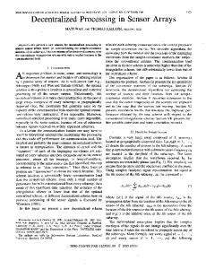
A Frequency-Domain SQUID Multiplexer for Arrays of Transition-Edge Superconducting Sensors. T. M. Lanting, Hsiao-Mei Cho, John Clarke, Matt Dobbs, Adrian ...
626
IEEE TRANSACTIONS ON APPLIED SUPERCONDUCTIVITY, VOL. 13, NO. 2, JUNE 2003
A Frequency-Domain SQUID Multiplexer for Arrays of Transition-Edge Superconducting Sensors T. M. Lanting, Hsiao-Mei Cho, John Clarke, Matt Dobbs, Adrian T. Lee, P. L. Richards, A. D. Smith, and H. G. Spieler
Abstract—We describe the development of a frequency-domain multiplexer (MUX) to read out arrays of superconducting transition-edge sensors (TES). Fabrication of large-format arrays of these sensors is becoming practical; however, reading out each sensor in the array is a major instrumental challenge. Frequency-domain multiplexing can greatly simplify the instrumentation of large arrays by reducing the number of SQUID’s (superconducting quantum interference devices) and wires to the low temperature stages. Each sensor is AC biased at a different frequency, ranging from 380 kHz to 1 MHz. Each sensor signal amplitude-modulates its respective AC bias frequency. An LC filter associated with each sensor suppresses Johnson noise from the other sensors. The signals are combined at a current summing node and measured by a single SQUID. The individual signals from each sensor are then lock-in detected by room temperature electronics. Test chips with fully lithographed LC filters for up to 32 channels have been designed and fabricated. The capacitance and inductance values have been measured and are close to the design goals. We discuss the basic principles of frequency-domain multiplexing, the design and testing of the test chips, and the implementation of a practical system. Index Terms—Bolometer, multiplexer, SQUID, transition-edge.
I. INTRODUCTION
T
HE next generation of cosmic microwave background (CMB) observations requires a major step up in sensitivity. This increase in sensitivity can be achieved with large arrays of several hundred to several thousand bolometers. The development of voltage-biased superconducting TES’s with strong electro-thermal feedback is a key technology that Manuscript received August 6, 2002. This work was supported by the National Science Foundation under Grant AST-00-96933, by NASA under Grant NAG5-11422, and by the Director, Office of Energy Research, Office of Basic Energy Science, Materials Sciences Division, U.S. DOE under Contract DE-AC03-76SF00098. The work of M. Dobbs and H. G. Spieler is supported by the Director, Office of Science, Office of High Energy and Nuclear Physics, U.S. DOE under Contract DE-AC03-76SF00098. T. M. Lanting and H. M. Cho are with the Physics Department, University of California, Berkeley, CA 94720 USA (e-mail: trevor@cosmology. berkeley.edu). J. Clarke is with the Physics Department, University of California, Berkeley, CA 94720 USA, and also with the Materials Science Division, Lawrence Berkeley Laboratory, Berkeley, CA 94720 USA. M. Dobbs, H. G. Spieler are with the Physics Division, Lawrence Berkeley Laboratory, Berkeley, CA 94720 USA. A. T. Lee is with the Physics Department, University of California, Berkeley, CA 94720 USA, and also with the Physics Division, Lawrence Berkeley Laboratory, Berkeley, CA 94720 USA. P. L. Richards is with the Physics Department, University of California, Berkeley, CA 94720 USA, and also with the Materials Science Division, Lawrence Berkeley Laboratory, Berkeley, CA 94720 USA, and the Space Sciences Laboratory, University of California, Berkeley, CA 94720 USA. A. D. Smith is with TRW Inc., Redondo Beach, CA 90278 USA. Digital Object Identifier 10.1109/TASC.2003.813973
provides well-controlled operating points and stable responsivity over large arrays. [1], [2] A second key technology is the development of fully lithographed fabrication techniques. [3] The remaining challenge is the readout of large arrays. Transition-edge sensors typically operate below 1 K and therefore reading out each sensor individually to room temperature would transmit too much heat along the readout wires. A possible solution is to multiplex the sensor signals in either the time-domain [4], [5] or the frequency-domain [6]. This paper discusses the development of a practical frequency-domain multiplexer for transition-edge sensors. II. BASIC PRINCIPLES An array of frequency-domain multiplexed sensors may be arranged as follows. We operate transition-edge sensors with an AC bias, with a different bias frequency applied to each sensor. When the sensor absorbs signal power, its resistance changes and modulates the signal current. This amplitude modulation transfers the signal spectrum to sidebands above and below the bias frequency. The very low noise and low input impedance of the SQUID makes it the obvious candidate for detecting the signal currents from the sensors. Since each sensor is operated at a different bias frequency, the signals corresponding to different sensors are uniquely distributed in frequency and can be combined in a common readout line. In the off-detector electronics the individual sensor signals are retrieved by a bank of frequency-selective demodulators. We can achieve our goal of reading out arrays of hundreds to thousands of sensors by using many of these multiplexer modules, each reading out approximately thirty sensors. In addition to the frequency-correlated signal current, each sensor contributes a wideband Johnson noise current. As a result, superimposed on the sideband spectrum associated with each bias frequency, the Johnson noise from all other sensors also appears. To avoid excessive noise buildup we reduce the bandwidth of the sensor circuit by introducing frequency selective components into each sensor circuit, as shown in Fig. 1. and the By appropriate choice of the circuit quality factor spacing between bias frequencies, the Johnson noise from adjacent channels can be kept arbitrarily low. In our multiplexer design, we use the current summing topology shown in Fig. 1 (We have previously explored a voltage summing topology [6]). The individual sensor circuits are joined in a common current summing node at the input of the readout amplifier. To maintain constant voltage on the sensor at the resonant frequency of its circuit, the input impedance of the amplifier must be much smaller than the sensor resistance,
1051-8223/03$17.00 © 2003 IEEE
LANTING et al.: A FREQUENCY-DOMAIN SQUID MULTIPLEXER FOR ARRAYS OF TRANSITION-EDGE SUPERCONDUCTING SENSORS
Fig. 1. Current summing multiplexer. The dotted box encloses the sensor circuits being multiplexed.
which is also required for efficient current summing. We then ensure a constant voltage bias level, provided that the bias , is much smaller than the sensor resistance, . resistor, The bias cross-talk is determined by the selectivity of the tuned circuits, provided the input impedance of the amplifier is constant over the frequency range of interest. Since the full spectrum of bias frequencies is applied to all sensors, the voltage developed across the amplifier input impedance only changes the bias level of the sensors.
III. CIRCUIT PARAMETERS A. Cross Coupling of Signal and Noise The frequency selectivity of the individual tuned circuits (Fig. 1) determines the cross-talk between channels. For a given bias frequency the maximum current flows through the channel whose resonance matches the bias frequency. However, the finite selectivity of the other channels allows a fraction of this carrier current to flow through them and be modulated by their respective sensors. The frequency dependence of the current flowing through the LCR circuit is given by:
(1)
is the normalized frequency, , Here, is the current at resonance ( ), and the circuit quality . factor At resonance the sensor is voltage-biased. The voltage ap. plied to the sensor is fixed and the bias power is Off-resonance, however, the voltage across the sensor depends given in (1) and the sensor power on the fractional current . Thus, the ratio of cross-talk power to on-resonance is power is equal to the square of the ratio of the cross-talk current to the on-resonance current. The total cross-talk is the sum of the contributions from all channels at a given frequency:
627
Analogously to signal cross-talk, noise from adjacent sensors is coupled into a given channel through the finite selectivity of the tuned circuits. Noise from the neighbor channels can be introduced in two ways. (i) Each sensor generates a wideband noise spectrum, shaped by the selectivity curve of the corresponding tuned circuit. Thus, noise from all sensors appears at a given bias frequency. (ii) The fractional carrier current of frequency flowing through the neighbor channels is modulated by the sensor noise and adds to the total noise in the sidebands associated with . The relative magnitude of this contribution is determined by the bias cross-coupling, as discussed above. The need for acceptable levels of bias cross-coupling and noise cross-coupling between multiplexed sensors determines the selection of channel frequency spacing. B. Bandwidth and Channel Spacing The maximum number of channels per output line is obtained with a constant bandwidth system using the minimum allowable to enbandwidth, which must be much greater than sure both constant voltage bias and electro-thermal stability, so , where is the decay time the channel bandwidth is constant of the sensor. The bandwidth of a LC tuned circuit is , where is the resonant frequency of the circuit. Thus, constant bandwidth implies that the circuit is propor, this is automatically fultional to frequency. Since filled if is kept constant. The spacing between individual frequency “bins” is determined by the required neighbor-channel attenuation. C. Determination of Circuit Parameters The circuit parameters for the multiplexer are thus interrelated and can be determined in the following sequence: 1) : The maximum is determined by the maximum freand the required bandwidth , . quency can be chosen at the expense of channel A lower density. 2) : The inductance is set by the adopted and the total resistance in the circuit (which we assume is dominated . by the sensor resistance, ): : The frequency spacing is determined by the al3) will couple into a lowable cross-talk. All neighbors given channel so that the cross-talk power to resonance power ratio is as in (2), and the noise ratio is . : The minimum frequency is given by the thermal 4) time constant of the sensor and by the maximum available capacitance together with the inductance calculated . in step 2: 5) These specifications determine the number of channels . per module, IV. CURRENT DESIGN
(2)
We have designed a 32-channel current-summing multiplexer using the configuration shown in Fig. 2. Each sensor circuit is
628
IEEE TRANSACTIONS ON APPLIED SUPERCONDUCTIVITY, VOL. 13, NO. 2, JUNE 2003
Fig. 3. The bias carrier signals can be suppressed to reduce dynamic range requirements. The dotted box encloses the sensor circuits being multiplexed.
spacing, bias and noise cross-coupling levels between channels are maintained. V. MULTIPLEXER READOUT Fig. 2. Layout of 8-channel MUX chip. The eight inductors surround a central capacitor core.
bandwidth-limited by a series LC (inductor and capacitor) combination. The fabrication was performed by TRW.1 The frequency range is from 380 kHz to 1 MHz with a nominal channel spacing of 20 kHz. For this test the multiplexer was subdivided into four 8-channel chips, whose resonant frequencies are interleaved so that within one chip the frequency spacing is 4 times the nominal spacing. The 8-channel chips can be used individually with 4-fold channel spacing or connected in parallel to form either a 16-channel or a full 32-channel multiplexer. Bond pads are provided to allow measurement of individual inductors and capacitors. Fig. 2 shows the layout of one chip; the die size is 1 cm. The capacitor dielectric is Nb O , formed by anodization of Nb. This yields a capacitance of 3 nF mm with very good uniformity. The inductors are implemented as square spirals. Since spiral inductors have a large fringing field, we reduce the sensitivity of the inductance to nearby conductors by utilizing the “transformer” geometry of the dc SQUID: the inductor spiral is tightly coupled to a square washer slit at one side. [8] The inductors all have the same value of 39.8 H and with a winding pitch of 4 m are 2.2 mm on a side. The capacitances range from 640 pF to 4.4 nF. At a frequency spacing of 500 (at 1000 kHz) the calof 20 kHz and a maximum culated noise degradation due to all neighbor channels is 9% and the bias cross-talk is less than 0.8%. For a given sensor the cross-talk is the sum of the squares of the currents at all the off-resonance frequencies divided by the square of the current at the resonance frequency. The devices have been fabricated, and the resonant frequencies of the circuits have been measured. We observed an absolute upward shift of 7% in all resonance frequencies compared to the design goals. This absolute shift is not critical for multiplexing. Since the shift does not affect channel frequency 1TRW
Inc., One Space Park, Redondo Beach, CA 90278.
A. SQUID Pre-Amplifier We use a SQUID to detect the current at the summing node of the multiplexer [9]. One of the major limitations with the use of SQUID’s for readout systems is their limited signal range. Because the peak excursion from the baseline magnetic flux across (where is the flux the SQUID is limited to quantum), a feedback system is needed to stabilize the operating point and to extend the SQUID’s dynamic range. We have designed a SQUID controller with a constant dynamic range over a signal bandwidth of 1 MHz. However, a funof 25 damental limit in our controller is the length of the wires between the SQUID and the flux locked loop. Even with an ideal, single-pole amplifier response, the phase shift from this length limits the gain-bandwidth product of the feedback loop. We are currently investigating whether, by restricting the length of the wire ( 20 cm round trip), our controller can achieve the desired gain, and thus dynamic range, over the 1 MHz bandwidth needed for our 32-channel multiplexer design. B. Carrier Nulling Since the peak signal into the SQUID is dominated by the bias carrier components, one can alleviate the dynamic range requirements by suppressing the carriers at the SQUID input. As all of the signal is in the sidebands, reducing the carrier does not affect signal recovery. This is illustrated in Fig. 3. Since the carrier levels set the dynamic range requirements, carrier suppression directly reduces the necessary loop gain. In the circuit shown in Fig. 3, the practical carrier attenuation is limited, since sensor loading by intense sources will change the sensor resistance. Adaptive feedback could be used to automatically optimize carrier nulling. For the current target array sizes, we may be able to avoid the complexity of carrier nulling. C. Readout Electronics The frequency-domain multiplexer reverts to full parallelism at the signal recovery stage, i.e., after current amplification by a SQUID. We have adopted a fully analog demodulation system, shown in Fig. 4. In principle, a digital signal processor could be
LANTING et al.: A FREQUENCY-DOMAIN SQUID MULTIPLEXER FOR ARRAYS OF TRANSITION-EDGE SUPERCONDUCTING SENSORS
629
VI. SUMMARY
Fig. 4.
Room temperature readout electronics.
used to retrieve all of the signals. However, at the high frequencies ( 1 MHz) we are using, this is presently not practical, although we are considering this option for future arrays. The composite signal stream is fed to a bank of phasesynchronous demodulators. The same carrier oscillators used to bias the sensors are used for demodulation. Thus, to first order, oscillator sideband noise cancels out. Direct digital synthesis oscillators provide both frequency and phase adjustability. The output of the synchronous detector feeds a low-pass filter and then a gated integrator. These integrators are all gated by the same clock, to ensure that all measurements in the array cover the same time intervals. The outputs of the gated integrators are multiplexed to a multichannel PC-based analog to digital converter with differential inputs to provide common-mode isolation. Digitization occurs within a time less than the integration interval, so there is no dead time. Our current design has 32 channels per multiplex module, so 1000 channels require about 30 modules, all of which are identical. All circuit functions can be performed by economical standard integrated circuits.
Although in principle one might read out several hundred sensors with one readout line, this introduces a significant singlepoint failure mode, so that 30–50 sensors per readout line appear to be a reasonable choice. Detailed designs are underway for arrays of 300–3000 superconducting transition-edge bolometers in next-generation CMB experiments. Frequency-domain multiplexers provide a practical method of reading out these arrays. As described in this paper, we have designed and built a high-frequency constant gain SQUID controller and a prototype 32-channel MUX with on-chip inductors and capacitors. We have verified that the LC circuits have the desired resonant frequencies. Component tests are nearing completion and we are preparing to multiplex transition-edge sensors. REFERENCES [1] A. T. Lee, P. L. Richards, S. W. Nam, B. Cabrera, and K. D. Irwin, “A superconducting bolometer with strong electrothermal feedback,” Appl. Phys. Lett., vol. 69, p. 1801, 1996. [2] S.-H. Lee et al., “A voltage-biased superconducting transition edge bolometer with strong electro- thermal feedback operated at 370 mK,” Applied Optics, vol. 37, p. 3391, 1998. [3] J. M. Gildemeister, A. T. Lee, and P. L. Richards, “Monolithic arrays of absorber-coupled voltage-biased superconducting bolometers,” Appl. Phys. Lett., vol. 77, p. 4040, 2000. [4] K. D. Irwin, “SQUID multiplexers for transition-edge sensors,” Physica C, vol. 368, pp. 203–10, 2002. [5] J. A. Chervenak et al., “Superconducting multiplexer for arrays of transition edge sensors,” Appl. Phys. Lett., vol. 74, pp. 4043–4045, 1999. [6] J. Yoon et al., “Single superconducting quantum interference device multiplexer for arrays of low-temperature sensors,” Appl. Phys. Lett., vol. 78, p. 371, 2001. [7] H. Spieler, LBNL-49 993. [8] J. M. Jaycox and M. B. Ketchen, “Planar coupling scheme for ultra-low noise DC SQUID’s,” IEEE Trans. on Magnetics, vol. MAG-17/1, pp. 400–403, 1981. [9] D. Drung, “High-performance DC SQUID read-out electronics,” Physica C, vol. 368, p. 134, 2002.