IEEE JOURNAL OF SOLID-STATE CIRCUITS, VOL. 41, NO. 1, JANUARY 2006
265
A Sub-10-ps Multiphase Sampling System Using Redundancy Li-min Lee, Student Member, IEEE, Daniel Weinlader, Member, IEEE, and Chih-Kong Ken Yang, Member, IEEE
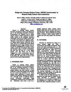
Abstract—This paper demonstrates a multichannel multiphase sampling system using a 700-MHz operating frequency to produce a base sampling rate of 7 GSample/s for each channel in a typical 0.18- m CMOS technology. An extra phase cluster with 10-ps sampling phase spacing is generated. To achieve this small phase spacing, static phase and voltage errors are digitally calibrated. Additionally, a redundancy technique is introduced in this paper to further halve the residual voltage error of the samplers. A third technique, i.e., “reference subtraction,” is applied to remove crosschannel correlated dynamic noise. The resulting phase spacing is only limited by the uncorrelated random noise in the system. With this fine sampling phase resolution, this system has the ability to measure cycle-to-cycle jitter in real time. Index Terms—Clock generation, delay-locked loops (DLLs), jitter, redundancy, sampling system, time-to-digital converter (TDC). Fig. 1. Operation of tester. Dashed arrows show an extra phase cluster for fine phase measurements and compensation.
I. INTRODUCTION
I
N ORDER to verify the functionality of modern multigigahertz digital systems, standalone digital testers must provides high-frequency test sequences, a system clock, and a means to verify the outputs of a device-under-test (DUT). With the increasing importance of phase errors and jitter at high frequencies, additional equipment is often used to acquire timing information of the data especially in real time. This paper addresses the challenges in producing accurately positioned sampling phases for sampling data up to 7 GHz, as well as the ability to sample real-time phase variations of 10 ps. Fig. 1 illustrates the basic functional blocks of a tester. Two of the critical components of a digital tester are a sampling front-end for data acquisition, and a clock generator providing accurate clocks to acquire data and to synchronize the DUT. For the clock generator, either a very high-frequency clock or multiple clock phases are used to sample signals with a high data rate. In order to acquire additional phase information of the signal from the DUT, a circuit that measures timing with even higher effective sampling rate than the data rate such as a time-to-digital converter (TDC) is used. Providing accurate phase positions and acquiring accurate real-time phase information of signals is challenging. The inherent device mismatch would cause static offsets and noise can also perturb sampled data limiting the achievable timing resolution. Several TDCs have been previously published [1]–[6].
Manuscript received May 4, 2005; revised August 8, 2005. This work was supported under UC-Micro 02-087. L. Lee and C.-K. K. Yang are with the Department of Electrical Engineering, University of California, Los Angeles, CA 90095-1594 USA (e-mail:
[email protected]). D. Weinlader is with Synopsys, Allentown, PA 18195 USA. Digital Object Identifier 10.1109/JSSC.2005.859883
The design in [3] uses a delay-locked loop (DLL) to divide the known reference period into smaller fractions as the measurement time unit. They obtain a 1-ns bin size from a 62-MHz clock by using a 16-stage delay line in a 1- m CMOS process. The sampling timing resolution of this method is inherently limited by the gate delay. Different techniques are implemented to further chop the time interval obtained from the main DLL for even finer time unit. In [2], an eight-stage RC delay line is used to arrive at a 48.8-ps time unit, which is roughly 1/3 of the gate delay in a 0.7- m CMOS technology. In [1], an extra DLL is used for generating finer time units. Several different delay chains are used after the second DLL to form the required sampling phases. The technique achieves 30-ps timing resolution, which is approximately 1/5 of a gate delay in a 0.6- m CMOS process. However, a longer delay chain results in more jitter. In both [2] and [1], the uncertainty of the timing measurement is comparable to the reported bin size. In [4] and [5], phase interpolators are implemented to generate a finer sampling phase resolution: 16 ps in a 25-GHz silicon bipolar process and 28 ps in a 0.25- m CMOS technology, respectively. However, the architectures do not push the resolution to the noise limit and, thus, the bin size is limited by the architecture rather than on-chip noise. The design in [6] uses a different architecture where the delay vernier concept is used, but instead of inserting delay elements, the inherent offset of an arbiter is used to create an effective phase difference. After determining the equivalent sampling phase of each arbiter, the system directly measures the timing difference between two signals. While [6] takes advantage of the inherent variation between arbiters to obtain the very fine timing resolution, the eventual resolution is difficult to predict before fabrication and the available measurement timing range
0018-9200/$20.00 © 2006 IEEE
266
IEEE JOURNAL OF SOLID-STATE CIRCUITS, VOL. 41, NO. 1, JANUARY 2006
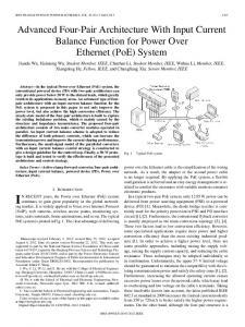
is small. Hence, the goal of our design is to build a data sampling system and TDC that pushes the timing resolution to the noise-limited boundary and still maintains the control and flexibility on positioning the sampling phases. The architecture of the system is described in Section II. The system is designed and fabricated in a 0.18- m logic CMOS technology. The circuits and architecture are both amenable to scale with technology. One of the focal points of the design is to investigate the finest possible phase resolution for multiple clock phases. The dashed arrows in Fig. 1 illustrate the fine phase cluster that is generated. As will be described in Section III, the architecture compensates for most sources of static and dynamic errors. The phase resolution of the system in this paper is ultimately limited by the residual quantization and the uncorrelated random noise of the system. Section III also describes the digital calibration technique and introduces a redundancy technique that further reduces the residual static error from quantization. Having fine multiphase resolution that is maintained, cross multiple input channels allow compensation for dynamic noise sources that are common to the multiple phases. These noise sources include input clock noise, reference noise, on-chip switching noise, and the noise from DUT shared between all channels. This compensation is described at the end of Section III and is referred to as “reference subtraction.” In order to achieve 8-ps resolution, several self-calibration techniques are used. Each source of residual errors is measured and tabulated. The methods of measurement are described in section IV. Finally, Section V describes the measurements of the entire phase generation system to demonstrate the effectiveness of the various techniques such as redundancy for reducing phase error, the self-calibration techniques, and reference subtraction. II. ARCHITECTURE OVERVIEW The implemented system consists of four main blocks, which are: 1) a precise clock generator; 2) samplers for data acquisition (only two channels are implemented in this test chip); 3) an SRAM for sampling data storage; and 4) a histogram counter for automatic phase positioning (Fig. 2). As shown in Fig. 2, the core of the clock generator is a fivestage DLL followed by two banks of digitally controlled phase interpolators with 3- and 6-bit digital control, respectively. Two sampling clocks are generated from each DLL delay element. An additional finer phase cluster of five phases is generated from the first delay stage of the DLL. By changing the digital settings of the two levels of interpolators, the timing of sampling clocks can be tuned and aligned with phase steps of less than 1/1000 of the cycle time. The digital tunability allows the system flexibility in positioning the cluster of clock phases and the spacing between the clock phases. All the multiphase clocks are used to drive two channels of data samplers. Each channel contains 16 data samplers. The voltage offset of each sampler can be digitally compensated with 3-bit digital control [7]. The sampled data are stored in a 64 128 bit SRAM for our prototype chip, and they are also sent to a 21-bit histogram counter through a multiplexer for automatic phase adjustment.
Fig. 2. Architecture of the system.
Fig. 3. Simplified over-sampling system with both: (a) dynamic noise and (b) static error sources marked on this figure.
III. DESIGN TECHNIQUES TO REDUCE PHASE-SPACING ERROR Fig. 3 shows a simplified sampling circuit. To obtain accurate timing information, the multiphase sampling circuit must maintain accurate sampling phase position and, consequently, phase spacing. The sources of phase spacing errors can be considered in two categories, which are: 1) dynamic noise and 2) static error. The dynamic noise, as shown in Fig. 3(a), consists of the jitter from the clock generator, the jitter from the data input itself, and the sampling noise from the comparators. The jitter from the clock generation includes the jitter from the reference clock, the DLL, and the buffers. Some components of the dynamic noise are shared by all sampling phases; e.g., the jitter of reference clock, the noise from supply and substrate,1 and the 1It is worthwhile to note that supply or substrate noise does not only cause correlated noise. As described in [8], the input-referred supply/substrate noise is a function of the offset and, consequently, a function of the device matching. Since the voltage offset is uncorrelated between sampling comparators, the resulting sampling noise from the supply/substrate noise is partially uncorrelated between channels. The same is true for the delay variation of each clock path due to supply/substrate noise. The part of the delay variation between clock paths differs due to the different device offset. According to simulation, with 5% supply noise, the caused uncorrelated noise seen between clock paths and comparators are 1 ps and 0.6 ps in our design, respectively.
6