N. Tang, W. Hong, J. H. Kim, Y. Yang and D. Heo, "A Sub-1-V Bulk-Driven Opamp With an Effective Transconductance-Stabilizing Technique," in IEEE Transactions on Circuits and Systems II: Express Briefs, vol. 62, no. 11, pp. 1018-1022, Nov. 2015. doi: 10.1109/TCSII.2015.2455471
A Sub-1V Bulk-Driven Opamp with Effective Transconductance Stabilizing Technique Nghia Tang, Student Member, IEEE, Wookpyo Hong, Student Member, IEEE, Jong-Hoon Kim, Youngoo Yang, Member, IEEE, and Deukhyoun Heo, Senior Member, IEEE Abstract—The effective transconductance (Gm) of a bulkdriven opamp can vary significantly with the input common mode voltage. This variation of Gm complicates frequency compensation and creates harmonic distortion. Thus, this paper presents a Gm-stabilizing technique to reduce the variation of Gm across the input common mode range (ICMR). The idea is to use a variable positive feedback structure to control Gm adaptively to the input common mode voltage. A low-voltage bulk-driven opamp with the proposed Gm-stabilizing technique has been implemented in a 0.18-μm n-well CMOS process. The opamp consumes 261 µW from a 900-mV supply voltage. The variation of Gm is reduced from 132% to 25% across the rail-to-rail ICMR. The measured DC gain is 76.8 dB, and the unity-gain bandwidth is 7.11 MHz when the opamp is loaded with 17-pF || 1-MΩ. Index Terms—rail-to-rail operational amplifier, bulk-driven input stage, effective transconductance, low voltage.
I. INTRODUCTION
T
he power supply voltage in integrated circuits has been reduced to 1 V and below to accommodate short-channel devices of advanced CMOS technologies. As a result, key analog circuits such as the operational amplifiers (opamps) are often required to have rail-to-rail operating voltage range. Several techniques have been explored to implement an opamp with rail-to-rail input common mode range (ICMR), such as complementary input stage [1-3], floating gate [4], depletion mode device [5], dynamic level shifter [6, 7] and bulk-driven input stage [8-15]. Each of these techniques has its advantages and disadvantages depending on the applications. For applications in which the supply voltage is below 1 V, the bulk-driven input stage is very effective in achieving rail-torail ICMR. A bulk-driven input stage is similar to its gatedriven counterpart, as shown in Fig. 1. The input signal is Manuscript received XXXXX. This work was supported in part by the Center for Design of Analog-Digital Integrated Circuits (CDADIC), the National Science Foundation (EECS-1231957 and CCF-1162202), the Joint Center for Aerospace Technology Innovation (JCATI), and the Technology Development Program of Korea Food Research Institute. N. Tang, W. Hong, and D. Heo are with the Electrical Engineering and Computer Science Department, Washington State University, Pullman, WA 99164 USA (email:
[email protected];
[email protected];
[email protected]). Y. Yang is with the School of Electronic and Electrical Engineering, Sungkyunkwan University, Suwon, Korea (email:
[email protected]). J.-H. Kim is with the Korea Food Research Institute, 516, Baekhyun-Dong, Sungnam 463-764, Republic of Korea (email:
[email protected]).
VDD
VDD Vb1
Vb1 VS
Vin+
Vin-
Vin-
Vin+
Vb2 (a) (b) Fig. 1. (a) Gate-driven PMOS differential input pair; (b) Bulk-driven PMOS differential input pair; Vb1 and Vb2 are bias voltages.
applied to the bulk (back gate or body) of an input device while the gate is biased to create a conducting channel between the source and drain. The effective transconductance (Gm) of an input stage is defined as the ratio of the output differential current to the input differential voltage. For a bulkdriven input stage, Gm depends on the bulk-transconductance of the input pair. Compared to its gate-driven counterpart, a bulk-driven opamp has lower gain and bandwidth because the bulk-transconductance of an input device is much smaller than its gate-transconductance. For a PMOS transistor, the bulktransconductance gmb can be expressed as
g mb g m
2 2 F VSB
,
(1)
where gm is the gate-transconductance, γ is the body effect coefficient, ΦF is the potential difference between the Fermi levels of the substrate and intrinsic silicon, and VSB is the source-bulk voltage. The source-bulk voltage VSB can be seen as the difference between the input common mode voltage VCM = (Vin+ + Vin-)/2 and the source-coupled node voltage VS in Fig. 1(b). When VCM moves from VDD to GND, VSB becomes larger, which increases gmb and Gm. As explained in [3], the variation of Gm as a function VCM complicates frequency compensation and increases harmonic distortion. The effective transconductance of a bulk-driven input stage can be increased by using partial positive feedback [10, 11] or an auxiliary differential pair [12]. However, there has been no attempt to reduce the variation of Gm across the ICMR in previous bulk-driven opamps [10-12]. Based on the structure presented in [10], this paper introduces a Gm-stabilizing technique to reduce Gm variation across the ICMR. The design of a low-voltage bulk-driven opamp with the proposed Gmstabilizing technique is described in section II. Section III presents experimental results to verify the performance of the
Copyright (c) 2015 IEEE. Personal use of this material is permitted. However, permission to use this material for any other purposes must be obtained from the IEEE by sending an email to
[email protected].
> REPLACE THIS LINE WITH YOUR PAPER IDENTIFICATION NUMBER (DOUBLE-CLICK HERE TO EDIT) < Input stage
VDD
Output stage
PB1
PB2
Vb
PB2
P5
Vindown
P1
P1
Vin+
Vb
P6
Vbp
R
up
P4
A
C
P6
Vout
B N4
P2
P2
N6
N4
N6
Iout-
Iout+ N1
N3
PO
P5
VS P3
2
N2
N2
N1
Vbn N5
N3
R
C
down N5
NO
GND
Fig. 2. Proposed bulk-driven opamp with Gm-stabilizing technique.
opamp, and conclusions are provided in section IV. II. PROPOSED BULK-DRIVEN OPAMP WITH GM-STABILIZING TECHNIQUE Fig. 2 illustrates the proposed bulk-driven opamp with the Gm-stabilizing technique. The bias circuits to generate Vb, Vbp, and Vbn are not shown for simplicity. A. Differential Mode Operation of the Bulk-Driven Input Stage In the input stage, the input signal is applied to the bulks of the input pair P1, and the gates are connected to GND to bias P1 in the saturation region. The Gm-stabilizing technique is implemented by NMOSs N1 – N4 and PMOSs P2 – P4. Transistors N1, N3 and N4 form a current mirror to deliver the differential currents to the output stage for single-ended conversion. Transistors N4 are biased in the triode region to provide a DC voltage shift and a low AC voltage gain from source to drain. Transistors N2 are connected to create a positive feedback loop. A small-signal equivalent circuit to analyze the differential mode operation of the input stage is illustrated in Fig. 3. The voltage gain of N4 is assumed to be unity to simplify the analysis. The voltages VA and VB at nodes A and B, respectively, can be derived as
VA gm,N1 gm,P 2 VB gm,N 2 gmb,P1Vin ,
(2)
VB gm,N 1 gm,P 2 VA gm,N 2 gmb,P1Vin ,
(3)
where gm,N1, gm,N2, and gm,P2 are the gate-transconductance of N1, N2, and P2, respectively, and gmb,P1 is the bulktransconductance of P1. To calculate the differential mode gain of the input stage, (3) is subtracted from (2), and rearranging the terms results in
ADM
g mb,P1 VA VB . Vin Vin g m,N 1 g m,N 2 g m,P 2
(4)
Therefore, the effective transconductance of the input stage can be estimated by Gm
g m, N 3 g mb, P1 I out I out , Vin Vin g m, N 1 g m, N 2 g m, P 2
(5)
I out g m,N 3VA
1 g m,P 2
g mb,P1Vin
g mb,P1Vin
VA
VB
1 g m,N 1
g m,N 2VB
g m,N 2VA
1 g m,P 2
I out 1 g m,N 1
g m,N 3VB
Fig. 3. Small-signal equivalent circuit of the proposed input stage to analyze differential mode operation; output conductance go of a device is assumed to be much smaller than transconductance gm.
where gm,N3 is the gate-transconductance of N3. The transconductance gm,P2 is controlled by current sources P3 and P4. The gate and bulk of P4 are biased by the source-coupled voltage VS. When the input common mode voltage VCM moves from VDD to GND, VS follows VCM, as shown in Fig. 4, which increases the bias current IP4 and the transconductance gm,P2. The variation of gm,P2 with respect to VCM can be derived as g m, P 2 VCM
CoxWP 2 g mb, P1 g m, P 4 g mb, P 4 , 2 LP 2 g m, P 2 g m, P1 g mb, P1
(6)
where gm,P1 is the gate-transconductance of P1, gm,P4 is the gate-transconductance of P4, gmb,P4 is the bulktransconductance of P4, WP2/LP2 is the width/length of P2, and Cox is the gate capacitance per unit area. It is observed that gm,P2 also increases with decreasing VCM. Thus, P2 and P4 can be designed such that to a first-order approximation, the variations of gm,P2 and gmb,P1 are matched to keep Gm relatively constant across the ICMR. It should be noted that the Gmstabilizing technique reduces Gm variation rather than making Gm absolutely constant. As a result, in spite of process, voltage, and temperature (PVT) effects on the absolute performance of the technique, the variation of Gm across the ICMR can still be effectively reduced. In our opamp implementation, gm,N1 and gm,N2 are made equal by matching N1 and N2. Thus, the constant current source P3 is needed to set a minimum gm,P2 to ensure a finite value of Gm in (5). It is worth noting that the simulated sourcebulk voltage VSB of the input pair reaches a maximum value of 390 mV when VCM is at GND, as shown in Fig. 4. Thus, the pn junction of the input pair is never turned on over the entire
> REPLACE THIS LINE WITH YOUR PAPER IDENTIFICATION NUMBER (DOUBLE-CLICK HERE TO EDIT)
REPLACE THIS LINE WITH YOUR PAPER IDENTIFICATION NUMBER (DOUBLE-CLICK HERE TO EDIT) < 25
800
Vout (mV)
700
20
out
600
15
500
10
400 300
5
200
0
100 0
Offset with 17 pF || 1 MOhm 0
100
200
300
400
500
Vin (mV)
600
700
800
-30
Input offset voltage (mV)
V with 17 pF || 1 MOhm out V with 50 pF || 3.3 kOhm
Voltage (V)
Normalized Transconductance
1.2 1 0.8 400
500
VCM (mV)
600
700
800
900
16
Coefficient of Variation (%)
Absolute values of Gm Normalized values of Gm
12 10 8 6 4 2 0
0
100
200
300
400
500
800
900
0.4 0.2 -5
0
5
10
15
20
Time (µs) Fig. 10. Measured step response of the opamp in unity-gain configuration.
(a) 14
700
0.6
0
300
600
0.8
1.4
200
500
1
1.6
100
400
Fig. 9. Measured total harmonic distortion (THD) of the opamp versus amplitude of 10-kHz and 100-kHz sinusoidal signals.
Without Gm stabilization, simulated With Gm stabilization, simulated With Gm stabilization, measured
0
300
Vin, pp (mV)
1.8
0.6
-45
-55 200
2.4
2
-40
-50
-5 900
Fig. 7. DC transfer characteristic of the proposed opamp.
2.2
10 kHz, 17 pF || 1 MOhm 100 kHz, 17 pF || 1 MOhm 10 kHz, 50 pF || 3.3 kOhm 100 kHz, 50 pF || 3.3 kOhm
-35
THD (dB)
900
4
600
700
800
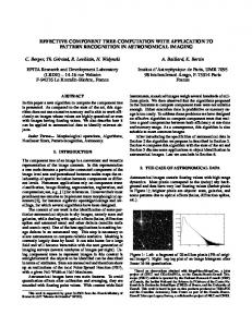
900
VCM (mV) (b) Fig. 8. (a) Normalized transconductance Gm versus input common mode voltage VCM; (b) Statistical variation of measured Gm across five chips.
where k is the Boltzmann’s constant, T is the temperature in Kelvin, K f is the flicker noise constant, and f is the noise frequency. Thus, the proposed input stage tends to have more noise than the one shown in [10]. III. EXPERIMENTS AND RESULTS The proposed bulk-driven opamp has been fabricated in a 0.18-µm n-well CMOS process. A chip micrograph is shown in Fig. 6. The opamp is measured with a 900-mV supply and two different load conditions: 17 pF || 1 MΩ and 50 pF || 3.3 kΩ. The DC transfer characteristic of the opamp is measured in unity-gain configuration. As shown in Fig. 7, the opamp demonstrates rail-to-rail ICMR and rail-to-rail output swing. The input offset voltage stays flat at 2 mV for ICMR from 300 mV to 800 mV. As the input voltage moves toward the supply rails, the offset changes due to saturation of the output stage.
To verify the Gm-stabilizing technique, the effective transconductance Gm is measured by applying a 100-mV sinusoidal signal and changing the common mode voltage from GND to VDD. Fig. 8(a) compares the normalized values of the measured Gm, the simulated Gm of the proposed opamp with Gm-stabilizing technique, and the simulated Gm of a normal bulk-driven opamp without Gm-stabilizing technique. The values of Gm are normalized to the Gm at VCM = VDD. The normal opamp has the same structure as shown in Fig. 2 except that P4 has its gate biased by Vb and its bulk connected to source. The effective transconductance of the normal opamp is seen to increase by 132% when VCM changes from VDD to GND. In contrast, the effective transconductance of the proposed opamp with Gm-stabilizing technique only varies by 25%. Fig. 8(b) shows the statistical variation in measured values of Gm across five chips, where the coefficient of variation is defined as the ratio of the standard deviation to the average value of Gm at each input common mode voltage. The measured absolute values of Gm can differ as much as 15%, but the normalized values suffer less variation, about 12%, from chip to chip. The 12% statistical variation is small compared to the achievable reduction in Gm variation across the ICMR, i.e., from 132% to 25%. The input bias currents of all five chips are measured below 1 nA across the rail-to-rail ICMR, proving that the bulk-source junctions of the input pair are not turned on. The total harmonic distortion (THD) of the opamp, shown in Fig. 9, was measured with 10-kHz and 100-kHz sinusoidal signals. The distortion increases rapidly when the signal approaches full rail-to-rail swing due to saturation of the
> REPLACE THIS LINE WITH YOUR PAPER IDENTIFICATION NUMBER (DOUBLE-CLICK HERE TO EDIT)