Nov 23, 2009 - We further discuss in some detail the background and ..... Schematic illustration of a defect supercell ( ) in an environment (env) of periodic.
Home
Search
Collections
Journals
About
Contact us
My IOPscience
Accurate prediction of defect properties in density functional supercell calculations
This content has been downloaded from IOPscience. Please scroll down to see the full text. 2009 Modelling Simul. Mater. Sci. Eng. 17 084002 (http://iopscience.iop.org/0965-0393/17/8/084002) View the table of contents for this issue, or go to the journal homepage for more
Download details: IP Address: 128.138.65.115 This content was downloaded on 14/07/2015 at 17:12
Please note that terms and conditions apply.
IOP PUBLISHING
MODELLING AND SIMULATION IN MATERIALS SCIENCE AND ENGINEERING
Modelling Simul. Mater. Sci. Eng. 17 (2009) 084002 (14pp)
doi:10.1088/0965-0393/17/8/084002
Accurate prediction of defect properties in density functional supercell calculations Stephan Lany and Alex Zunger National Renewable Energy Laboratory, Golden, CO 80401, USA
Received 8 July 2009, in final form 13 October 2009 Published 23 November 2009 Online at stacks.iop.org/MSMSE/17/084002 Abstract The theoretical description of defects and impurities in semiconductors is largely based on density functional theory (DFT) employing supercell models. The literature discussion of uncertainties that limit the predictivity of this approach has focused mostly on two issues: (1) finite-size effects, in particular for charged defects; (2) the band-gap problem in local or semi-local DFT approximations. We here describe how finite-size effects (1) in the formation energy of charged defects can be accurately corrected in a simple way, i.e. by potential alignment in conjunction with a scaling of the Madelung-like screened first order correction term. The factor involved with this scaling depends only on the dielectric constant and the shape of the supercell, and quite accurately accounts for the full third order correction according to Makov and Payne. We further discuss in some detail the background and justification for this correction method, and also address the effect of the ionic screening on the magnitude of the image charge energy. In regard to (2) the band-gap problem, we discuss the merits of non-local external potentials that are added to the DFT Hamiltonian and allow for an empirical band-gap correction without significantly increasing the computational demand over that of standard DFT calculations. In combination with LDA + U , these potentials are further instrumental for the prediction of polaronic defects with localized holes in anion-p orbitals, such as the metal-site acceptors in wide-gap oxide semiconductors. (Some figures in this article are in colour only in the electronic version)
1. Introduction For the theoretical description of defects and impurities, the central quantity of interest is the defect formation energy �HD , which determines, for example, the defect concentrations in equilibrium [1–5], and the thermodynamic transition energies between the different possible charge states of electrically active defects [6]. Notwithstanding the ground state formalism of density functional theory (DFT), one can also determine optical excitation or recombination 0965-0393/09/084002+14$30.00
© 2009 IOP Publishing Ltd
Printed in the UK
1
Modelling Simul. Mater. Sci. Eng. 17 (2009) 084002
S Lany and A Zunger
energies from �HD , as long as the transitions occur as a result of the exchange of electrons with a distant reservoir, such as the band-edge states hosting the free carriers, or if the optically excited state is the lowest energy state of a given symmetry [7]. Thus, the formation enthalpy �HD is the most decisive quantity for the functionality of semiconducting materials in regard to the presence and properties of defects or impurities. Within a supercell model, the formation energy is calculated as � �HD,q (EF , µ) = [ED,q − EH ] + n α µα + q · E F , (1) α
where ED,q is the total energy of the supercell containing the defect in the charge state q and EH is the respective supercell energy of the host without the defect. The chemical potentials µα describe the energy of the atomic reservoir of the atoms α removed (nα = +1) or added (nα = −1) to the host crystal when the defect is formed. For charged defects (q �= 0), the Fermi energy EF describes the energy of the reservoir for the electrons, which is typically considered to range between the valence band maximum (VBM) and the conduction band minimum (CBM), except for conditions of extremely high doping, e.g. in transparent conducting oxides [4], where EF can reach a few tenths of an electronvolt into the conduction band. For the accurate calculation of �HD,q one needs to pay special attention to two different types of uncertainties, i.e. those that arise due to finite-size effects within supercell models, and those that arise due to inaccuracies in the underlying approximation for the energy functional. Regarding finite-size effects (1), it has been recognized that the average potentials of the charged defect calculation and that of the unperturbed host need to be aligned [3, 8], and that corrections are needed to account for the electrostatic interaction of the periodic images of the charged defects. Leslie and Gillian [9] suggested using the screened Madelung-energy of point charges compensated by a background to correct the image interaction. Makov and Payne [10] later extended this picture by introducing a third order term accounting for the interaction of the delocalized part of the defect-induced charge with the screened point-charge potential of the images. However, numerous applications over the past decade have drawn a mixed picture about the appropriateness of such corrections [11–24]. Only recently, were we able to demonstrate [25] by calculation of large supercells up to 1728 atoms that a very good convergence can be obtained when the third order image charge correction is combined with a potential alignment procedure, and when finite-size effects that are not related to the presence of a net charge are excluded or addressed separately. Note also that in a recent work of Freysoldt et al [26], very good convergence has been achieved as well with a method that does not utilize the expansion of Makov and Payne [10], but instead calculates the respective interaction energies from the calculated charge densities and the electrostatic potentials of the defect and of a reference (e.g., pure host) supercell. In this work, we discuss in more detail than before the background and the justification for the potential alignment and the image charge corrections, and address the issue of electronic versus ionic screening for the image charge interaction. Regarding the errors associated with the functional (2), a lot of attention has been paid to the ‘band-gap problem’ occurring in calculations of semiconductors and insulators based on the local density or generalized gradient approximation (LDA or GGA). In general, defect formation energies are affected by the band-gap problem in two ways. First, defect states may occur outside the band gap as resonances within the continuum of host states, whereas after opening of the band gap they should occur inside the gap. As a result of the incorrect placement of the defect level relative to the host band, electron-occupied defect states can incorrectly spill the electron into the conduction band [27], or hole defects can incorrectly spill the hole into the valence band. In this case, even the calculated charge density is incorrect 2
Modelling Simul. Mater. Sci. Eng. 17 (2009) 084002
S Lany and A Zunger
leading to an uncontrolled error in �HD . Second, in the case of charged defects, �HD,q depends linearly on the Fermi level (see equation (1)), which is bounded by the band-edge energies. When the band gap is changed, the range of formation energies between EF = EVBM and EF = ECBM changes accordingly. In order to cope with the band-gap problem for defect calculations, numerous methods and schemes of band-gap corrections for defect calculations have been proposed [6, 18, 22, 25, 28–34]. We also note that beyond the band-gap problem per se, the underlying approximation of the DFT functional may of course also affect the defect states directly, e.g. leading to a qualitatively wrong description of localized hole states in compound semiconductors [35–39]. Furthermore, the chemical potentials µα that enter the expression for the formation energy in equation (1) are bounded by the respective elemental phases of the atoms α. Here, the incomplete error cancellation between the total energies of the semiconductor compound and that of the elemental phases in general affects the defect formation energies. Improved bounds for the chemical potentials can be obtained through the optimized elemental reference energies of [40]. For the purpose of band-gap corrected defect calculation, much effort has recently been focused on post-LDA methods such as hybrid DFT [21, 24, 41–44], the related screened exchange (sX) method [45], GW [44, 46–48] or quantum Monte Carlo [49]. Common to these methods is that they are computationally much more demanding than standard DFT calculations. Also, hybrid DFT does not necessarily yield very accurate defect levels when the parameters are adjusted so as to match the experimental band gap [50]. Thus, there exists a desire for self-consistently band-gap corrected methods that are not significantly more expensive than standard LDA. For example, an empirical correction for the band gap can be achieved using parametrized potentials that are added to the DFT Hamiltonian [51, 52]. A similar band-gap opening effect is obtained by the LDA + U method, when applied not only to cation-d states, but also to cation-s or anion-s states [23, 25, 33, 53], or by an atomicorbital based variant [32, 54] of the self-interaction correction (SIC) [55]. In order to achieve a flexible means for empirical adjustment of the band structure, we recently [27] introduced nonlocal external potentials (NLEP) whose implementation is similar to the respective LDA + U potentials, but which do not depend on the orbital occupation. Here, we describe more details of this method and discuss possible extensions. 2. Finite-size effects due to charged defects 2.1. The need for potential alignment When periodic boundary conditions are applied, the total energy of a system with a net charge is ill-defined due to the divergence of the electrostatic potential. Depending on the particular implementation of the energy expression, e.g. that of [56] for pseudopotential methods, the calculated total energy E follows Janak’s theorem dE(ni ) = ei , (2) dni upon variation of the occupation number ni of the highest occupied state i with the eigenvalue ei . In particular, the energy of a hole at the VBM in a unit of a semiconductor host (H) with N electrons is then obtained as lim [EH (N ) − EH (N − 1)] = eVBM ,
N →∞
(3)
i.e. the hole energy equals the eigenvalue of the VBM in the limit of a infinite system (in practice, this result can be calculated within a small unit cell and fractional charges [34]). Thus, the eigenvalue eVBM can be used as the reference energy for the electron reservoir in equation (1), 3
Modelling Simul. Mater. Sci. Eng. 17 (2009) 084002
S Lany and A Zunger
i.e. EF = eVBM + �EF , where �EF denotes the position of the Fermi level within the semiconductor band gap (0 < �EF < Eg ). Since the (otherwise divergent) average electrostatic (el) potential within the cell is conventionally set to zero within the pseudopotential momentum-space formalism [56], i.e. Vel (G = 0) = 0, the eigenvalues are defined only up to an undetermined constant. Whereas the total energy of a charge-neutral system is a well-defined quantity [56], the ‘charged energies’ depend on the same undetermined constant as the eigenvalues, which can be seen from equations (2) and (3). While the omission of the G = 0 term of the Fourier expansion is often described as in effect introducing a compensating background charge, it is important to note that the charge compensation occurs only in the potential, but a background charge density is usually not explicitly introduced into the calculation. Note that if a compensating charge density were introduced, the resulting overall charge-neutral system should have a welldefined total energy and not depend on the undetermined constant [25]. While the energy of the ‘charged cell + background density’ in principle can be calculated, it is usually not desirable to have the interaction energy of the background with all N electrons and Z ionic charges included in the total energy. In order to obtain a physically meaningful formation energy �HD,q without explicitly introducing the interaction with a background density, one can use the total energy calculated with the usual energy expression [56] for which equation (2) holds, and then correct for the undetermined offset by ensuring that the undetermined constants in ED,q and in eVBM are consistent. That is, one needs to restore the relative positions of the average potential in the calculations of the defect (affecting ED,q ) and the pure host (affecting eVBM ). This is achieved by means of a ‘potential alignment’ (pa) correction that is added to the formation energy: �Epa (D, q) = q · �Vpa ,
(4)
where �Vpa is the potential alignment between the defect and the host calculation, respectively. For practical calculations we use as reference potentials the atomic-site electrostatic potentials VDα 1 , serving as ‘potential markers’. The potential alignment �Vpa = (VDα − VHα ) is then α determined as the average difference between VD,q in the defect supercell and the respective α VH in the pure host. The immediate neighbors of the defect are excluded from averaging, since their atomic potentials can be affected by the chemical interaction with the defect. For the case 3+ of the As vacancy VAs in GaAs, which we used in [25] as a test case to study finite-size effects, α (r) − VHα (r) as a function of the distance r from figure 1 shows the potential difference VD,q the defect. If the supercell is large enough (e.g., 1000 atoms in figure 1(a)), the atomic-site potentials clearly reflect the shape of the long-ranged screened electrostatic potential due to the charged defect (and its images). 2.2. Correction of image charge interactions The leading (first order) correction term for the electrostatic interaction energy between the images (i) of charged supercells is the screened Madelung-like lattice energy of point charges [9], �Ei1 =
q 2 αM , 2εL
(5)
where L = �−1/3 is the linear supercell dimension (supercell volume �), ε is the dielectric constant and αM is the appropriate Madelung constant for the respective supercell geometry. 1
α The atomic-site potentials VD,q are determined as the average electrostatic potential in a small sphere around an atom [57].
4
Modelling Simul. Mater. Sci. Eng. 17 (2009) 084002
S Lany and A Zunger
Figure 1. The difference in the atomic-site potentials VGa and VAs between a supercell containing a 3+ vacancy VAs and the defect-free host, shown for 1000 atom supercell (a) and a 64 atom supercell (b).
Addressing primarily the case of molecules in vacuum (ε = 1), Makov and Payne derived an expression for a third order correction term by decomposing the total charge into a point charge plus an extended (e), net neutral density ρe (r ). In this case, the energy correction due to the energy of ρe (r ) in the potential of the point-charge images (quadrupole–monopole interaction) is 2πqQr �Ei3 = , (6) 3εL3 where � Qr = d3 rρe (r) r 2 (7) �
is the second radial moment of the extended charge density. Since, for the case of molecules in vacuum, ρe (r ) is confined within the supercell, the interaction energy between ρe (r ) and its images (without the point-charge contribution) scales as O(L−5 ) and is neglected. When translating these results for molecules in vacuum to the case of defects in solids (ε � 1), the defect-induced electronic charge density, �ρD (r ) = ρD (r ) − ρH (r ) (ρD =charge density in the defect supercell; ρH = density in the unperturbed host supercell) takes the place of the extended density ρe (r ) in equation (7), and the total energy correction �Ei = �Ei1 +�Ei3 is calculated as the sum of the first and third order terms, equations (5) and (6), respectively. In [25], we demonstrated for a number of defects in GaAs that the image charge correction calculated in this way, in conjunction with the potential alignment (see above), provides for excellent convergence of the �HD,q with respect to the supercell size, being well converged already for typical cell sizes of 64 atoms. The results for the triply charged As vacancy 3+ VAs in the zinc-blende lattice of GaAs are shown in figure 2, where the atomic relaxation 5
Modelling Simul. Mater. Sci. Eng. 17 (2009) 084002
S Lany and A Zunger
3+ Figure 2. The formation energy �H of the VAs defect in GaAs (EF = EV , As-rich conditions) as a function of the inverse linear supercell dimension 1/L = �−1/3 (� = supercell volume, �0 = volume of the 2 atom GaAs unit cell). (Modified from [25].)
was constrained so as to exclude finite-size effects originating from elastic energies [25]. Less satisfying convergence was observed only for the face-centered cubic (FCC) supercell symmetries (e.g., 16, 54, 128 atoms), which was attributed to the fact that in these geometries, the defects are aligned along the (1 1 0) zig-zag chains, which promote strong direct defect– defect interactions. Consequently, these supercells are generally not recommended for defect calculations. While the image charge correction according to equations (5)–(7) proved very successful, there exist a few conceptional issues regarding the application in semiconductors, which we address now. First, in their original paper, Makov and Payne surmised that the density entering the integration of Qr (see equation (7)) should contain only that part of �ρD (r ) that does not arise from electronic screening. However, we found in [25] that Qr is actually dominated by contribution to �ρD (r ) arising from the screening response upon introduction of a charged defect into the semiconductor host. Excluding this part would greatly reduce the magnitude of �Ei3 and significantly worsen the convergence behavior. Second, since the defect density �ρD (r ) is largely due to the screening response of the host, it is not confined within the supercell, but extends toward the space between the images. Thus, superficially, it seems unjustified to neglect the interaction energy between the extended densities �ρD (r ), i.e. the quadrupole–quadrupole interaction as was done in the case of confined density ρe (r ) for molecules in vacuum. In order to resolve these apparent conceptional conflicts, we now discuss in more detail the image charge interactions in the presence of a dielectric medium: The total (electron + ion) charge density in the defect supercell, can be written as ρHtot (r) + �ρp (r ) + �ρD (r ), where �ρp (r ) is the point-charge-like contribution due to the ionic substitution, which is assumed here to include also a compensating background. The image charge correction is the difference between the electrostatic interaction energy of the supercell with an environment (env) of unperturbed host supercells minus the interaction energy of the supercell with an environment 6
Modelling Simul. Mater. Sci. Eng. 17 (2009) 084002
S Lany and A Zunger
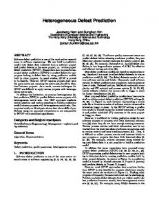
Figure 3. Schematic illustration of a defect supercell (�) in an environment (env) of periodic images (left) or in an environment of host cells (right).
of identical defect supercells (see figure 3): � � �Ei = − dr 3 (ρHtot (r ) + �ρp (r ) + �ρD (r ))
env
�
dr �3
�ρp (r � ) + �ρD (r � ) . |r − r � |
(8)
Under the approximation that the supercell is large enough so that each unit cell of the pure host appears as a neutral object on the scale of the supercell (despite being modulated within a unit cell), we can neglect the interaction energy of ρHtot (r ) with the total defect-induced density [�ρp (r � ) + �ρD (r � )] in the image supercells. Thus, excluding the term involving ρHtot (r ), we can express equation (8) as the sum of interactions between the subsystems ρp and ρD : �Ei = −(Ep,p + Ep,D + ED,D ).
(9)
At this point we observe that (i) so far no screening has been invoked and (ii) equation (9) contains the quadrupole–quadrupole term ED,D which cannot be neglected because the density �ρD (r ) is not confined within the supercell. However, considering that �ρD (r ) essentially reflects the screening response of the host upon introduction of the charged defect [25], we can env interpret the integral over the volume ‘env’ in equation (8) as the screened potential Vscr (r) created by the point charges in the supercell images and their compensating background: � env �Ei = − dr 3 (�ρp (r ) + �ρD (r ))Vscr (r). (10) �
env The interaction energy between screened point-charge potential Vscr (r) with �ρp (r ) and with �ρD (r ) corresponds to the first and third order terms, equations (5) and (6), respectively, when the screening response of the host is included in �ρD (r ). Thus, comparing equation (10) with equation (9), we see that after electronic screening is accounted for, the quadrupole–quadrupole does not enter anymore. It is therefore justified to truncate the expansion beyond the third order term despite the fact that the delocalized part of the defect-induced charge extends up to the border of the supercell. Regarding the role of the compensating background, we again note that the total energy does not include the (undesired) electrostatic interaction of the background with the full electron+ion system (∼N charges), since the background is not explicitly included in the charge density of the supercell (see above). Rather, as seen from equation (8) after dropping the term with ρHtot , the only interaction energy involving the background is that between the background and the defect-induced charge (∼q charges) in the surrounding supercells. This artificial interaction energy is corrected for by the image charge interaction according to equations (5) and (6).
7
Modelling Simul. Mater. Sci. Eng. 17 (2009) 084002
S Lany and A Zunger
Table 1. The factors csh for the simplified expression, equation (11) of the image charge correction, given for the supercell geometries SC, FCC, BCC, HCP and a 3×3×2 multiple of the ideal HCP cell. Supercell geometry
csh
SC FCC BCC HCP HCP (3 × 3 × 2)
−0.369 −0.343 −0.342 −0.478 −0.365
2.3. Simplified expression for the image charge correction The observation that the delocalized part of the defect-induced density, �ρD (r ), is dominated by the screening response of the host has the important consequence that the second radial moment Qr entering the third order correction term, equation (6), is proportional to q and to L2 , such that the �Ei3 scales effectively as ∝ q 2 /L instead of the nominal ∝q/L3 scaling implied by equation (6). Thus, the full first plus third order image charge correction �Ei can be accounted for by a simple scaling of the first order Madelung-like term [25]. We now use this finding to give a simplified expression for �Ei . Considering that the electronic charge that accumulates close to the defect due to dielectric screening is drawn more or less homogeneously from the entire supercell [25], the defect-induced charge density is approximately �ρD (r > lscr ) ≈ �1 q(1 − ε −1 ) for distances r from the defect that are larger than the screening length lscr , i.e. at those distances that dominate the integration of Qr (due to the r 2 factor in the integrand of equation (7)). Thus, we can express the full image charge correction approximately by the first order correction �Ei1 , equation (5), times a factor that depends only on the dielectric constant ε and on the shape (sh) of the supercell: �Ei = [1 + csh (1 − ε −1 )]�Ei1 .
(11)
The shape factors csh can easily be calculated using equations (5)–(7), by performing the integration in equation (7) over the Wigner–Seitz cell with a constant charge density. In table 1, we give the numerical values of csh for simple cubic (SC), face-centered cubic (FCC), bodycentered cubic (BCC), hexagonal close packed (HCP) cells and for a 3 × 3 × 2 HCP supercell. For the cubic supercells, the values of csh are close to −1/3. The ideal HCP geometry has a larger csh (absolute value) which is due to its rather anisotropic shape (aspect ratio). The more isotropic 3 × 3 × 2 supercell, as used below for defect calculations in wurtzite ZnO, however, has a value of csh similar to the cubic geometries. Thus, we see that equation (11) reduces to �Ei ≈ 2/3�Ei1 if two conditions are fulfilled, i.e. (i) the dielectric constant is sufficiently large (ε � 1) and (ii) the supercell is approximately isotropic. This explains the earlier empirical observation that �Ei ≈ 2/3�Ei1 when the third order term was calculated from the actual defect-induced density �ρD determined from the self-consistent defect calculation [32]. 2.4. The role of ionic screening In order to examine the scaling behavior of the electrostatic interactions, some previous works [20, 25, 26] have used a constrained relaxation (e.g., only nearest neighbors [25]), so as to eliminate the effect of elastic energies from the finite-size scaling. In this situation, the interaction between the charged defect and its images is only electronically screened, i.e. one would use the static electronic (e) dielectric constant ε = εe to determine the image charge correction in equations (5), (6) and (11). In practical applications, however, one is generally interested in the defect properties including full relaxation. In this situation, ionic screening 8
Modelling Simul. Mater. Sci. Eng. 17 (2009) 084002
S Lany and A Zunger
2+ defect in ZnO (E = E , O-rich) in GGA, Figure 4. Finite-size scaling of �H for the VO F V calculated with constrained atomic relaxation (diamonds) and with full relaxation (circles). The image charge correction is determined using ε∞ = 5.0 or ε0 = 10.3.
also contributes to the screening of the image charge energy, so that the total (electronic+ionic), i.e. the low-frequency dielectric constant ε = ε0 is appropriate, proposed that the supercell dimension is sufficiently large compared with the effective screening length. Using 72, 192 and 576 atom supercells of the wurtzite lattice, we show in figure 4 the finite-size scaling of VO2+ in ZnO, where there exists a larger difference between ε0 and εe than, e.g., in GaAs. We determine here εe = 5.0 from a calculation with a periodically modulated external field, in agreement with previous calculations based on density functional perturbation theory [58, 59], and we use ε0 = 10.3 from [58]. In a calculation with constrained atomic relaxation, as determined for the nearest and next nearest neighbor shells in the 72 atom cell, we find that finite size effects are very well eliminated if we apply the image charge correction according to equation (11) (with respective factors csh for the actual cell geometries), and if we use the electronic dielectric constant ε = εe (figure 4). Similarly, converged formation energies for the fully relaxed situation are obtained, if we instead use the low-frequency dielectric constant ε = ε0 . The difference, �Erel = −0.94 eV, accounts for the (elastic) relaxation energy when atomic relaxation beyond the second shell is taken into account. For illustration, we further show in figure 4 the formation energies for the fully relaxed supercell, but using εe (only electronic screening). In this case, considerable finite-size effects remain, and we emphasize that the apparent relaxation energy, obtained without considering the reduction of the image charge energy due to ionic screening, is considerably smaller than the true relaxation energy, in particular for small cells, e.g. the apparent relaxation energy is only �Erel = −0.18 eV in the 72 atom cell (see figure 4). Thus, in general, it is important to account for the ionic contribution to the screening when determining the magnitude of the image charge correction. 3. Correction of the band-gap problem 3.1. The aim of self-consistent band-gap correction Ever since the first predictions of defects in semiconductors within the LDA [6, 60], the ‘band-gap problem’ pervasively troubled the literature on the theoretical prediction of defect properties, and a range of band-gap correction methods emerged, many of which apply energy 9
Modelling Simul. Mater. Sci. Eng. 17 (2009) 084002
S Lany and A Zunger
corrections to the defect formation energy but still rely on the self-consistent LDA defect calculation [6, 18, 22, 25]. In many cases, however, the very small band gap leads to a spurious hybridization between the defect states and the host bands, leading to a qualitatively wrong description of the defect state [27]. In these cases, the gap correction within the self-consistent calculation is indispensable. In order to correct the band structure of the semiconductor host within the self-consistent calculation, Christensen [51] introduced additional potentials, which were empirically adjusted to match the experimental band structure. In a similar spirit, the LDA + U method [61–64], which is typically used to improve the LDA description of cation-d states, was applied for band-gap corrected defect calculations, where it acts to open the band gap when using negative values for U on anion-s states [33, 53], or very large positive values for U on cation-s states [23, 25]. Self-consistently band-gap corrected defect calculations have also been performed [65] on the basis of SIC [55] in a simplified implementation [32, 54] that, similar to LDA + U , employs atomic projections. Recently, hybrid-DFT calculations which mitigate the band-gap problem by a mixing of the density functional and Hartree– Fock exchanges became quite popular for defect calculations [21, 24, 41–45], although they are computationally still much more demanding than standard DFT calculations. Based on perturbation theory arguments, Perdew et al [66] suggested a parameter of 25% for the uniform mixing of the exact exchange for typical molecules, which, by extension, is also often preferred for solids. On the other hand, in practical applications of hybrid DFT to semiconductors or insulators, the mixing parameter is often also empirically chosen to match the experimental band gap [24, 67]. The uncertainties arising from the question how to mix the exact and the GGA exchange are avoided in GW, which, however, for the purpose of defect calculations is so far only feasible for determining the quasi-particle energies [44, 46], but not for self-consistent total-energy calculation. 3.2. Empirical NLEP Given that fully parameter-free and accurate post-LDA methods such as GW or quantum Monte Carlo [49] remain very demanding for defect systems which typically require a system size on the order of 100 atoms, an alternative route is to devise computationally effective parametrized functionals that can be employed for very large systems or for a very large number of calculations, once the parameters have been fitted to high-accuracy reference calculations, or to experiment. In this vein, non-self-consistent (semi-) empirical pseudopotentials [68] can be applied to large scale problems such as quantum dots and nanostructures without the band gap problem [69]. In order to achieve a self-consistent band-gap correction that can be applied to defects, including different charge states and atomic relaxation, we recently introduced NLEP, which are parameterized in the atom type α and the angular momentum l [27]. The implementation of these potentials into the projector-augmented wave (PAW) method [70, 71] employs the PAW projectors pi and the all electron partial waves φiAE which depend on an index i that comprises the atomic site α, the angular momentum numbers l, m and an index k for the reference energy used to determine the partial waves φiAE [71]. Thus, the functional form of the NLEP potential is analogous to the LDA + U potential [72]: � NLEP NLEP AE Vˆα,l = |pi φiAE |Vα,l |φj pj |, (12) i,j NLEP but contrary to LDA + U , the potential strength parameters Vα,l are free parameters that do not depend on the orbital occupancies. In equation (12), the sum runs only over those iandj that contain the atom type α and angular momentum l for the specified NLEP potential.
10
Modelling Simul. Mater. Sci. Eng. 17 (2009) 084002
S Lany and A Zunger
A further difference between NLEP and LDA+U is that the total-energy contribution due to the NLEP potential is not derived from a model for the electron–electron interaction. Whereas LDA + U is derived from a (screened) Hartree–Fock-like interaction [61, 62], the NLEP are treated as simple external potentials. Since, the interaction energy between the electrons and an external potential is contained in the sum of occupied eigenvalues, no additional terms for the total energy are needed. For example, we used in [27, 73] the NLEP method to predict the defect levels of transition metals in ZnO and In2 O3 , where the main contribution to the band-gap correction comes from the repulsive NLEP potential for cation-s states. According NLEP NLEP to equation (12), e.g. the NLEP potential VZn -s leads to an energy contribution EZn-s in the sum over the occupied eigenvalues en of the corresponding Kohn–Sham orbitals ψn : � � NLEP NLEP
ψn |pi φiAE |φjAE pj |ψn , (13) EZn -s = VZn-s n=occ. i,j
which equals simply the potential strength times the Zn-s partial charge nZn-s : NLEP NLEP EZn -s = VZn-s nZn-s .
(14)
In order to achieve an optimal overall description of the band structure and structural properties, we used in [27, 73] not only NLEP potentials for Zn-s, but also for Zn-p and for O-s/p. A drawback of the NLEP method is that the static NLEP potentials act to change the charge NLEP density in an unphysical way. For example, while the repulsive VZn -s potential increases the band gap in ZnO by shifting the Zn-s-like conduction band states to a higher energy, it also acts to reduce the Zn-s partial charge that exists due to the partially covalent character of the Zn–O bonds. Thus, the band-gap correction by NLEP renders ZnO more ionic than in LDA or GGA, which is probably unphysical. While we confirmed for the cases studied in [27, 73] by variation of the NLEP parameters that the reduction of the Zn-s partial charge does not significantly affect the predicted defect levels of the transition metals, one would in general like to achieve the band-gap correction without adverse effects on the charge density. Possible extensions of the NLEP potentials, e.g. by including the dependence on the energy parameter k NLEP in the NLEP parameters, Vα,l,k , are expected to accomplish this [74]. Apart from the empirical band-gap correction, the NLEP potentials proved useful for the prediction of polaronic hole states in oxides [37, 39], such as the acceptor states introduced by LiZn or the cation vacancy VZn in ZnO, and the metal-site acceptors in other oxides such as In2 O3 and SnO2 . While it is generally known that such localized hole states are incorrectly described in standard DFT functionals as rather delocalized states that spread over all oxygen ligands [35–39], the quantitative prediction of the acceptor states remains challenging. For example, the LDA + U potential, e.g. in the form of [64], U Vm,σ = U eff ( 21 − nm,σ ),
(15)
qualitatively restores the correct localization of the acceptor state of AlSi in SiO2 on just one O ligand when it is applied on O-p states [37]. However, it simultaneously distorts the underlying host band structure in a rather uncontrolled way, because the O-p partial charge nO−p depends sensitively on the integration radius used for LDA +U [38]. In order to avoid such ambiguities, we introduced in [38] a hole-state potential of the form Vhs = λhs (1 − nm,σ /nhost ),
(16)
where nhost is the O-p partial charge of the unperturbed (defect-free) oxide host and λhs is a potential strength parameter. The specific form, equation (16), of the hole-state potential can be easily constructed by the combination of the NLEP and LDA + U potentials, using eff = λhs /nhost UO−p
(17) 11
Modelling Simul. Mater. Sci. Eng. 17 (2009) 084002
S Lany and A Zunger
and NLEP VO−p = λhs (1 − 0.5/nhost ),
(18)
and it ensures that the underlying host band structure is not affected [38], in contrast to LDA + U . Further, the strength parameter λhs is determined by the fundamental requirement that the energy must be a piecewise linear function of the (fractional) number of electrons between integers [75–77]. Using this condition, the correction of the localized acceptor state (without band-gap correction) and the restoration of the correct splitting between occupied and unoccupied anion-p sublevels can be achieved fully non-empirically. Applying the holestate correction in [35] to the metal-site acceptors in ZnO, In2 O3 and SnO2 , we obtained much deeper acceptor levels than in standard LDA or GGA calculations, which curbs the expectations to achieve p-type doping by acceptor-like point defects in wide-gap oxide semiconductors. Studying the behavior of Zn vacancies in the series of Zn chalcogenides (ZnO, ZnS, ZnSe, ZnTe), we further demonstrated in [39] that the metallic-type band structure predicted in GGA for the host + vacancy system changes into an insulating-type akin to the situation in a Mott insulator, when the correct linear behavior of the energy as a function of the electron number is restored. Thus, quite unexpectedly, electronic correlation effects beyond LDA or GGA that cause such a transition from metallic to insulating behavior exist not only in anion-p shells of first row elements, such as oxygen, but also in much heavier anions such as Te. The qualitative change of the electronic structure of the vacancy defects has important consequences for the so-called d0 magnetism [78]. Corroborating the conclusions of Droghetti et al [79] based SIC, we found in [39] that the magnetic interaction between VZn vacancies is impeded when the localization of the holes is correctly described. 4. Conclusions Finite-size effects due to charged defects in supercell calculations can be corrected by considering potential alignment and image charge corrections simultaneously. The expansion up to third order in the inverse linear supercell dimension, as suggested by Makov and Payne, provides a very accurate correction of the image charge energy if the full defect-induced density, including the contribution from dielectric screening, is considered for the calculation of the third order term. We further provided a justification for the truncation of the expansion after the third order term, despite the fact that the defect-induced density is not confined within the supercell. Based on the observation that the defect-induced density is actually dominated by the screening response of the host, we suggest a simple but accurate approximation of the full third order image charge correction, being expressed as the respective first order term times a factor that depends only on the shape of the supercell and the dielectric constant. We further demonstrated that the low-frequency dielectric constant determines the magnitude of the image charge correction if atoms within the entire supercell are allowed to relax, whereas the ionclamped (electronic-only) dielectric constant is more appropriate if the atomic relaxation is restricted to a small volume around the defect. With respect to the band-gap problem, we highlighted the desire for self-consistently band-gap corrected methods whose demand in computational resources does not significantly exceed that of standard DFT calculations. For this purpose, we described the addition of the NLEP to the DFT Hamiltonian, which carries the prospect of combining the benefits of empirical pseudopotentials and self-consistent DFT calculations. Apart from the application for band-gap correction, we have used these NLEP potentials also in combination with LDA+U to define a ‘hole-state potential’ for polaronic, localized anion-p holes which are otherwise incorrectly described in standard DFT functionals. The correct description of the localization 12
Modelling Simul. Mater. Sci. Eng. 17 (2009) 084002
S Lany and A Zunger
of the anion-p hole and of the energy splitting between occupied and unoccupied sublevels has quite important ramifications for acceptor doping of wide-gap oxide semiconductors and for the prospects of d0 magnetism. Acknowledgments This work was funded by the US Department of Energy, Office of Energy Efficiency and Renewable Energy, under Contract No DE-AC36-08GO28308 to NREL. References [1] [2] [3] [4] [5] [6] [7] [8] [9] [10] [11] [12] [13] [14] [15] [16] [17] [18] [19] [20] [21] [22] [23] [24] [25] [26] [27] [28] [29] [30] [31] [32] [33] [34] [35] [36] [37] [38] [39] [40] [41] [42] [43]
Kr¨oger F A 1974 The Chemistry of Imperfect Crystals (Amsterdam: North-Holland) Zhang S B and Northrup J E 1991 Phys. Rev. Lett. 67 2339 Laks D B, van de Walle C G, Neumark G F, Bl¨ochl P E and Pantelides S T 1992 Phys. Rev. B 45 10965 Lany S and Zunger A 2007 Phys. Rev. Lett. 98 045501 Lany S, Osorio-Guill´en J and Zunger A 2007 Phys. Rev. B 75 241203 Baraff G A and Schl¨uter M 1985 Phys. Rev. Lett. 55 1327 Dabrowski J and Scheffler M 1989 Phys. Rev. B 40 10391 Mattila T and Zunger A 1998 Phys. Rev. B 58 1367 Leslie M and Gillian M J 1985 J. Phys. C: Solid State Phys. 18 973 Makov G and Payne M C 1995 Phys. Rev. B 51 4014 Schultz P A 2000 Phys. Rev. Lett. 84 1942 Lento J, Mozos J-L and Nieminen R M 2002 J. Phys.: Condens. Matter 14 2637 Gerstmann U, De´ak P, Rurali R, Aradi B, Frauenheim T and Overhof H 2003 Physica B 340–342 190 Segev D and Wei S-H 2003 Phys. Rev. Lett. 91 126406 Limpijumnong S, Zhang S B, Wei S-H and Park C H 2004 Phys. Rev. Lett. 92 155504 van de Walle C G and Neugebauer J 2004 J. Appl. Phys. 95 3851 Shim J, Lee E-K, Lee Y J and Nieminen R M 2005 Phys. Rev. B 71 035206 Schultz P A 2006 Phys. Rev. Lett. 96 246401 Castleton C W M, H¨oglund A and Mirbt S 2006 Phys. Rev. B 73 035215 Wright A F and Modine N A 2006 Phys. Rev. B 74 235209 Gali A, Hornos T, Son N T, Janz´en E and Choyke W J 2007 Phys. Rev. B 75 045211 Janotti A and van de Walle C G 2007 Phys. Rev. B 76 165202 Paudel T R and Lambrecht W R L 2008 Phys. Rev. B 77 205202 Oba F, Togo A, Tanaka I, Paier J and Kresse G 2008 Phys. Rev. B 77 245202 Lany S and Zunger A 2008 Phys. Rev. B 78 235104 Freysoldt C, Neugebauer J and van de Walle C G 2009 Phys. Rev. Lett. 102 016402 Lany S, Raebiger H and Zunger A 2008 Phys. Rev. B 77 241201 Svane A and Gunnarsson O 1990 Phys. Rev. Lett. 65 1148 Zhang S B, Wei S-H and Zunger A 2000 Phys. Rev. Lett. 84 1232 Stampfl C, van de Walle C G, Vogel D, Kr¨uger P and Pollmann J 2000 Phys. Rev. B 61 R7846 Zhang S B, Wei S-H and Zunger A 2001 Phys. Rev. B 63 075205 Filippetti A and Spaldin N A 2003 Phys. Rev. B 67 125109 Persson C and Zunger A 2005 Appl. Phys. Lett. 87 211904 Persson C, Zhao Y J, Lany S and Zunger A 2005 Phys. Rev. B 72 035211 Pacchioni G, Frigoli F, Ricci D and Weil J A 2000 Phys. Rev. B 63 054102 Lægsgaard J and Stokbro K 2001 Phys. Rev. Lett. 86 2834 Nolan M and Watson G W 2006 J. Chem. Phys. 125 144701 Lany S and Zunger A 2009 Phys. Rev. B 80 085202 Chan J A, Lany S and Zunger A 2009 Phys. Rev. Lett. 103 016404 Lany S 2008 Phys. Rev. B 78 245207 To J, Sokol A A, French S A, Kaltsoyannis N and Catlow C R A 2005 J. Chem. Phys. 122 144704 Patterson C H 2006 Phys. Rev. B 74 144432 Sokol A A, French S A, Bromley S T, Catlow C R A, van Dam H J J and Sherwood P 2007 Faraday Discuss. 134 267 [44] Stroppa A and Kresse G 2009 Phys. Rev. B 79 201201 13
Modelling Simul. Mater. Sci. Eng. 17 (2009) 084002 [45] [46] [47] [48] [49] [50] [51] [52] [53] [54] [55] [56] [57] [58] [59] [60] [61] [62] [63] [64] [65] [66] [67] [68] [69] [70] [71] [72] [73] [74] [75] [76] [77] [78] [79]
14
S Lany and A Zunger
Xiong K, Robertson J and Clark S J 2006 J. Appl. Phys. 99 044105 Weber J R, Janotti A, Rinke P and Van de Walle C G 2007 Appl. Phys. Lett. 91 142101 Ma Y and Rohlfing M 2008 Phys. Rev. B 77 115118 Bockstedte M, Marini A, Gali A, Pankratov O and Rubio A 2009 Mater. Sci. Forum 600–603 285 Batista E R, Heyd J, Hennig R G, Uberuaga B P, Martin R L, Scuseria G E, Umrigar C J and Wilkins J W 2006 Phys. Rev. B 74 121102 Lany S and Zunger A, unpublished Christensen N E 1984 Phys. Rev. B 30 5753 Wei S H and Zunger A 1993 Phys. Rev. B 48 6111 Walsh A, da Silva J L F and Wei S H 2008 Phys. Rev. Lett. 100 256401 Pemmaraju C D, Archer T, S´anchez-Portal D and Sanvito S 2007 Phys. Rev. B 75 045101 Perdew J P and Zunger A 1981 Phys. Rev. B 23 5048 Ihm J, Zunger A and Cohen M L 1979 J. Phys. C: Solid State Phys. 12 4409 See VASP the Guide http://cms.mpi.univie.ac.at/VASP/ Wu X, Vanderbilt D and Hamann D R 2005 Phys. Rev. B 72 035105 Fuchs F, Furthm¨uller J, Bechstedt F, Shishkin M and Kresse G 2007 Phys. Rev. B 76 115109 Lindefelt U and Zunger A 1982 Phys. Rev. B 26 846 Anisimov V I, Zaanen J and Andersen O K 1991 Phys. Rev. B 44 943 Anisimov V I, Solovyev I V, Korotin M A, Czyzyk M T and Sawatzky G A 1993 Phys. Rev. B 48 16929 Liechtenstein A I, Anisimov V I and Zaanen J 1995 Phys. Rev. B 52 R5467 Dudarev S L, Botton G A, Savrasov S Y, Humphreys C J and Sutton A P 1998 Phys. Rev. B 57 1505 Pemmaraju C D, Hanafin R, Archer T, Braun H B and Sanvito S 2008 Phys. Rev. B 78 054428 Perdew J P, Ernzerhof M and Burke K 1996 J. Chem. Phys. 105 9982 Alkauskas A, Broqvist P, Devynck F and Pasquarello A 2008 Phys. Rev. Lett. 101 106802 Wang L W and Zunger A 1995 Phys. Rev. B 51 17398 Wang L W, Franceschetti A and Zunger A 1997 Phys. Rev. Lett. 78 2819 Bl¨ochl P 1994 Phys. Rev. B 50 17953 Kresse G and Joubert J 1999 Phys. Rev. B 59 1758 Bengone O, Alouani M, Hugel J and Bl¨ochl P 2000 Comput. Mater. Sci. 17 146 Raebiger H, Lany S and Zunger A 2009 Phys. Rev. B 79 165202 Lany S and Zunger A, unpublished Perdew J P, Parr R G, Levy M and Balduz J L 1982 Phys. Rev. Lett. 49 1691 Perdew J P, Ruzsinszky A, Csonka G I, Vydrov O A, Scuseria G E, Staroverov V N and Tao J 2007 Phys. Rev. A 76 040501 Mori-S´anchez P, Cohen A J and Yang W 2008 Phys. Rev. Lett. 100 146401 Coey J M D 2005 Solid State Sci. 7 660 Droghetti A, Pemmaraju C D and Sanvito S 2008 Phys. Rev. B 78 140404