An Application Specific Memory Characterization Technique for Co-processor Accelerators Sadaf R Alam and Jeffrey S Vetter Oak Ridge National Laboratory alamsr,
[email protected]
Abstract Commodity accelerator technologies including reconfigurable devices provide an order of magnitude performance improvement compared to mainstream microprocessor systems. A number of computeintensive scientific applications, therefore, can potentially benefit from commodity computing devices available in the form of co-processor accelerators. However, there has been little progress in accelerating production-level scientific applications using these technologies due to several programming and performance challenges. One of the key performance challenges is performance sustainability. While computation is often accelerated substantially by accelerator devices, the achievable performance is significantly lower once the data transfer costs and overheads are incorporated. We present an application-specific memory characterization technique for an FPGA-accelerated system that enabled us to reduce data transfer overhead by a factor of five for a production-scale scientific application. Our proposed technique extends to applications that exhibit similar memory behavior and to co-processor accelerator systems that support data streaming, pipelining, and overlapped execution.
1. Introduction Commodity accelerator technologies including reconfigurable devices and graphical processing units (GPUs) provide an order of magnitude performance improvement compared to mainstream microprocessor systems with high power efficiencies. Current GPU devices for instance offer over 30x compute power for single-precision floating-point calculations. In addition, these devices are presently available in the form of co-processor accelerators, and are expected to be available in tightly-coupled systems in near future. AMD Torrenza and Fusion technologies are examples in which Opteron processor will be connected over the Hypertransport link [1]. A number of floating-point intensive scientific applications can potentially benefit
Melissa C Smith Clemson University
[email protected]
from co-processor accelerators in a power and cost effective manner as these devices become widely available. One of the key challenges in exploiting the performance of these co-processor accelerators is how to minimize data transfer costs between the host system and the co-processor devices. While computation is often accelerated significantly with accelerator devices, the achievable performance is substantially lower once the data transfer costs and overheads are included [20]. In this study, we present an application-specific memory characterization technique for an FPGAaccelerated system. This technique enabled us to reduce data transfer overhead for a scientific application by over a factor of 5. We classify large data structures in the application according to their memory (read and write) characteristics and access patterns. This classification in turn enabled us to sustain a speedup of over three for a production level scientific application called AMBER [2] on a FPGAaccelerated system by SRC Computers Inc. [7]. Our proposed technique can be extended to other applications that exhibit similar memory behavior and to co-processor accelerator systems that support data streaming and pipelining, and allow overlapped execution between the host and the accelerated device. Outline of the paper is as follows: section 2 provides a background to the accelerated application and the target system; an overview of related research is presented in section 3; implementation details and initial performance assessment is presented in section 4; section 5 explains the application specific memory characterization scheme and its impact on performance; and conclusions and future plans are described in section 6.
2. Background Numerous applications use molecular dynamics (MD) calculations for bio-molecular simulations. These applications include AMBER [2], CHARMM [12], GROMACS [5], LAMMPS [16], and NAMD [14]. MD and related techniques can be defined as a
computer simulation methodology where the time evolution of a set of interacting particles is modeled by integrating the equation of motion. The underlying MD technique is based upon the law of classical mechanics, and most notably Newton’s law, F = ma [15]. The MD steps performed in AMBER consist of three calculations: determining the energy of a system and the forces on atom’s centers, moving the atoms according to the forces, and adjusting temperature and pressure. Most MD models treat atoms classically as points with mass and charge. The atomic points interact with other atomic points through pair-wise interactions from chemical bonds, electrostatic interactions and van der Waals interactions. A typical biomolecular simulation contains atoms for solute, ions, and solvent molecules. The force on each atom is represented as the combination of the contribution from forces due to atoms that are chemically bonded to it and non-bond forces due to all other atoms. The simplified overall energy equation is E ( potential ) =
∑ f (bond ) + ∑ f (angle) +
bonds
angles
⎛ Aij Bij f (d − torsions ) + ∑∑ ⎜ − 6 + 6 ∑ ⎜ r rij dihedral j =1 i =1 ⎝ ij N
N
⎞ N N ⎛⎜ qi qj ⎞⎟ ⎟ + ∑∑⎜ ⎟ j =1 i =1 ⎝ rij ⎟⎠ ⎠
where the first three terms are the bonded terms and the latter two are referred to as non-bonded terms. The non-bond energy is broken into two contributions: van der Waals and electrostatic interactions. The number of bonds, bond angles, and bond dihedrals during the classical simulations are kept constants. For a medium system, there are only a few thousand bonds and angles compared to millions of the non-bonded interactions; the calculations involving the bonded terms are extremely fast on available systems. The double sum of the non-bond terms makes the number of these calculations scale with an order of N2, where N is the number of atoms. Simulation of larger systems (larger N) is therefore extremely expensive. In order to address these aforementioned issues, we are investigating the acceleration of an MD calculation called the Particle Mesh Ewald (PME) method on FPGA-accelerated computing systems using a highlevel language, Fortran—AMBER is implemented in Fortran and uses message-passing (MPI) communication infrastructure. Currently, the SRC MAPstation [7], Cray XD1 [3], SGI RASC [6], DRC [4] and XtremeData [9] systems are all available with FPGA devices. DRC and XtremeData systems provide a very high bandwidth connection to the AMD Opteron processor over the Hypertransport link [1]. The SRC platforms are the only systems that provide a coherent programming environment allowing users to program the FPGA using Fortran and C programming
languages. Since the sander module in AMBER is written in Fortran 90, we targeted the SRC-6E MAPstation® taking advantage of the support for Fortran programming. The Series E MAPstation pairs a dual 2.8 GHz Xeon® microprocessor with a MAP® processor consisting of two user-configurable Xilinx® XC2VP100 FPGA devices [8] running at 100 MHz, a control processor, and seven 4MB SRAM banks referred to as On-Board Memory (OBM).
3. Related Work A number of related efforts to develop MD codes on reconfigurable hardware platforms have been reported in the literature. In [13], the authors implement a basic MD system focused on the motion updates and the O(N2) force terms (both Coulombic and L-J forces and multiple atom types) using hardware design techniques. The authors study the relationship between precision and quality of MD simulations and report that it is possible with reconfigurable devices to trade off unneeded precision for computing resources. Implementation on a COTS system yielded accelerations ranging from 31x to 88x with respect to a PC implementation, depending on the size of the FPGA and the simulation accuracy. Similarly, in [11], the authors implemented a novel single atom type MD system with VHDL on a Transmogrifier 3 (TM3) system. The focus is on the implementation of the L-J force calculator with problem specific implementations. To reduce complexity, the implementation uses fixed-point representations varying between 22 and 76 bits for all values within the MD system. The author’s results show that this implementation closely tracked the higher precision software implementation with an error of less than 1% between consecutive time steps. The authors extrapolate that with better FPGA memory organization and faster FPGAs, a speedup of 40x to 100x over a microprocessor implementation can be achieved. In [19], the authors use the SRC development suite Carte® to implement a tightly coupled MD simulation kernel (not a complete MD software package such as AMBER) on the SRC-6E MAPstation. Like our approach, the important tasks of an MD simulation are analyzed and partitioned such that the most computeintensive tasks are executed in the reconfigurable hardware and the rest are executed on the generalpurpose processor. Even though only a portion of the simulation is accelerated in the MAP, the singleprecision implementation achieves a 2x speedup over the software baseline running on the MAPstation host.
Neither [11], [12], nor [19] are concerned with the problem of accelerating existing, production-level, MD simulation software nor have they been tested with more than a few thousand particles. The most closely related work comes from [18] where the authors implement a simplified version of an MD algorithm in NAMD [14], an MD simulation package, on the SRC6 MAPstation. While their implementation does trace the steps involved in porting a large-scale scientific code to FPGA-enabled systems, they do not cover memory analysis and characterization methodology and its impact on achievable performance, which is presented in this article.
4. Implementation The Ewald method in the molecular dynamics (MD) calculations expands the simple sum of Coulomb’s Law (electrostatic) terms into the sum of direct and reciprocal Ewald calculations and a correction function. Except for the error correction function, the direct sum is identical to the sum in the cutoff method that calculates electrostatic potential energy. The reciprocal sum is a major part of the electrostatic energy that the direct sum misses due to the correction factor. The reciprocal sum is approximated using Fast Fourier Transform (FFT) with convolutions on the grid where charges are interpolated on the grid points. Table 1 provides the percentage of execution time (for 10000 time steps or production-scale simulations) for four different protein experiments on an Intel dual 2.8 GHz Xeon system. The direct sum accounts for over 80% of execution time. The reciprocal Ewald calculation takes less than 13% of the total execution time. Taken together, these calculations account for over 95% of total execution time on a single processor system. Number of atoms 23558 61641 143784 194262
Direct Ewald Time (%) 82.61 86.88 87.12 86.47
Reciprocal Ewald Time (%) 16.66 12.56 12.34 12.92
Table 1: Time spent in the direct and reciprocal Ewald calculations (% of total execution time). We further break down the runtime cost in the Direct Ewald calculation into five functions (see Table 2). Calls to functions f1, f2, and f3 are made once every time step; calls to f4 depend on the number of atoms in the system; f5 is called twice as many times as f4. The functions f4 and f5 are both called from within f3. Considering the runtime distribution and the logic capacity of our target FPGA devices, we map f3, f4 and f5 onto the co-processor accelerators.
Number of atoms f1 (% of total) f2 (% of total) f3 (% of total) f4 (% of f3) f5 (% of f4)
23558
61641
143784
194262
0.1% 0.4% 82.1% 86.1% 18.8%
0.1% 0.5% 86.2% 85.9% 20.9%
0.2% 0.5% 86.4% 88.4% 17.9%
0.2% 0.5% 85.8% 88.4% 17.9%
Table 2: Time spent in the five functions of the Direct Ewald calculations.
4.1. Mapping Details The characteristics of FPGA devices allow for techniques such as deep pipelining, concurrent execution, and data streaming making them an ideal target for a diverse range of scientific calculations, since no other processing device offers a combination of these capabilities in a flexible manner. We exploit these features with SRC-6E and Carte constructs to achieve a higher speedup. We accelerate the direct Ewald calculation on the FPGA devices. The nested calls to functions f3, f4, and f5 in the original code are replaced by a single invocation to a SRC MAP (FPGA implementation) function that then performs the calculations of the three functions on the FPGA devices. The only differences between the original and FPGA-accelerated implementation (in Fortran) is the additional calls for data transfers between the host processor and the on-board memory of the MAP and the FPGA-specific constructs for parallel execution of the code blocks.
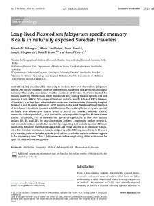
Figure 1: Control and data paths between the host processor and the FPGA chips. A schematic of the co-processor accleration process is shown in Figure 1. The host processor oversees the control and data movement between the host and the FPGA devices. However, once the devices are setup, the primary FPGA chip invokes the DMA operations. Since a single pipeline can span multiple FPGA chips, the data transfers between the FPGA chips are controlled by the primary FPGA chip. Note that all control and data transfer calls shown in Figure 1 can be active simultaneously. In addition, the SRC systems have multiple data ports; for instance, three 64-bit
elements can be transferred between the two FPGA chips in a single clock cycle. Additionally, we fully exploit the six on-board memory banks of the SRC-6E system. Since there is a latency associated in accessing a memory bank in consecutive clock cycles, frequently-used read-only arrays can be replicated on multiple memory banks. This technique not only permits consecutive clock cycle reads but also permits independent access by both FPGA devices. Deep pipelining techniques on FPGA devices allow users to describe the parallelism in terms of a producer-consumer programming paradigm. A producer-consumer relationship can be between: (1) host and the primary FPGA chip; (2) primary FPGA chip and secondary FPGA chip; and (3) parallel sections within a single FPGA chip. A parallel section construct in the SRC programming permits task parallelism, i.e., multiple computation and data transfer tasks can be executed on a device simultaneously. In addition to block data transfer, the FPGA devices allow for streaming data is transfer between the producer and consumer devices. The data transfer overheads and latencies, in most cases, can be concealed using the deep pipelining and streaming techniques of the FPGA programming, as long as there is sufficient work (computation) available to hide these latencies. The performance of a pipeline will be the latency of the most-expensive (largest latency) parallel section.
4.2. Performance Analysis We measured the performance of the FPGAaccelerated code for two test cases namely jac and HhaI. The jac benchmark is part of the AMBER version 8.0 release and it contains 23,558 atoms. HhaI is a protein-DNA system that contains 61,641 atoms. The microprocessor-based performance is measured on the SRC host processor system, described in section 2. The system imposes a fixed 100 MHz clock frequency restriction on the FPGA devices. We should also note that the performance of the FPGA devices on our target SRC-6E system is not representative of the full capabilities of the current-generation FPGA devices (current-generation FPGA devices have more logic and memory capacity and are capable of operating at higher frequencies) [21]. Nevertheless, we demonstrate the potential for FPGA acceleration for an important class of applications on these devices. In order to analyze the performance behavior, we used the SRC-6E performance analysis and debugging tools to measure the runtime contributions of the key sections of the accelerated code. Runtimes for three sections are measured separately: (1) time to setup the
MAP or calling overhead; (2) compute time; and (3) data transfer times. The time to setup the MAP has an additional cost (~0.3 milliseconds) for the first invocation; in subsequent invocations this cost is then comparable to the cost of the regular Fortran function calls. The data transfer time includes the time to receive data from the host and to send results back to the host. Compute time is the computation time spent on the two FPGA devices including the time to transfer data between the two chips. Our experiments and measurements reveal that the data transfer overheads offset the performance gains in a naïve implementation and the penalties are higher for the larger problem, HhaI. The compute only speedup increases with the problem size or the number of atoms, 3.3x and ~4x, respectively. At the same time, the data transfer overheads increase with the problem size, thereby reducing the application speedup to less than one. At this stage, we concluded that the memory access requirements needed to be characterized in order to sustain performance on the FPGA devices.
5. Memory Characterization We considered and evaluated a number of techniques to reduce the data transfer times. First, data can be pre-fetched and post-stored to hide data transfer latencies. Additionally, multi-threading techniques using pthreads or OpenMP allow users to transfer large arrays while the compute thread is processing before the accelerated function is invoked. Second, data transfers to the FPGA can be pipelined and overlapped using the streaming directives provided in the SRC Programming Environment. Although some of these techniques are applied in the first implementation of the code, we recognize that further performance optimization can be achieved by carefully overlapping and pipelining all array transfers. Finally, algorithmspecific optimizations can be achieved by characterizing the memory access behavior in the accelerated code. We employ the third approach since it also leverages the other optimization techniques. There are eight large arrays that are transferred to the co-processor for acceleration of the PME calculations. These include image coordinate arrays (over 7 Kbytes) and force coordinates (~4 Kbytes) for the jac benchmark. Overall, the naïve implementation requires transfer of approximately 24 Kbytes per invocation. On the SRC 6-E system, the sustain payload bandwidth is 2.8 GBytes/sec (utilizing input and output 1.4 Gbytes/second bandwidth). Hence, the data transfer overhead accounted for over two-third of the total execution time per simulation time step.
5.1. Data Structure Classification In order to exploit the SRC Programming Environment data transfer utilities, particularly for streaming data and overlapping host and accelerated device execution, we classified the arrays into the following categories according to their read and write characteristics and memory access behaviors: • Initialized once arrays: these arrays a are initialized typically in the beginning of the application run. The cost of these arrays is amortized over a production-scale run. • Read-only: these arrays are not modified within the accelerated code. This classification helps in eliminating output cost. • Write-only: these arrays are modified by the accelerated application only. No read cost is associated with these arrays. • Read and write: these arrays a re modified not only in the accelerated code but also in the calculations performed by the host. Read and write costs are associated with these arrays. • Conditional read/write: In MD calculations, not all arrays are updated at every time step. Typically, there is a variable that determines when some arrays will be modified. The host processor can send the condition variable and the accelerated code can then determine when a read and write operation should be invoked. • Local: local variables in the accelerated calculations need not be transferred. • Pre-fetch: this memory access feature allows for pre-fetching data before the invocation of accelerated calculation. Hence, this cost is not included in the data transfer and overhead costs of the accelerated code. • Delayed write: like pre-fetch, this cost is hidden. The accelerated code can send completion signal to the host prior to sending updated values. We found all of the above-mentioned classes represented in the arrays for the direct PME calculations. Since no existing tool has the capability of classifying arrays into these categories, we manually identified and classified arrays, in other words sampling of variables that are used in the accelerated calculation. This process involved detailed and tedious profiling and debugging of the entire application since data modifications could take place in any part of the application execution. Furthermore, the categories enable us to identify overheads that can be eliminated in an RC implementation. The application code under consideration is optimized for conventional computing platforms where arrays may be copied to improve
performance on these platforms; these same copy semantics cause unnecessary and costly overheads on RC systems. Therefore, the task of array characterization is crucial for performance optimization on RC systems. The larger arrays (image coordinates) are conditionally read approximately every 20-25 function invocations, and these are not written by the FPGA devices. Hence, we were able to modify the FPGA function call such that a condition parameter is passed to the device indicating when to invoke DMA calls to access the arrays. Furthermore, we found that the large force arrays are not read elsewhere in the code after the direct PME calculations; therefore, writing back to the processor via DMA calls is not required. Moreover, we identified that not all the arrays are needed before the start of the three-way nested loop and we can delay the transfer of these arrays and allow the computation to proceed by overlapping the loop calculation and streaming data transfers. Implementation of the accelerated PME calculation is further modified according to memory access classification and characterization. This new implementation, however, does not include any modification to the AMBER source code on the host to exploit additional benefits from multithreading using pthreads or OpenMP. Only the Fortran source code for the FPGA-accelerated calculations is modified in order to reduce the unnecessary data transfer overheads. Amazingly, the modified code resulted in a very significant reduction in the data transfer costs; the data transfer costs that previously accounted for over 70% of the total execution time, is now less that 5% of the total execution time resulting in sustained accelerated performance on the FPGA devices.
5.2. Performance Improvement In order to estimate the improvement due to memory characterization, we compare time-to-solution for the accelerated calculation before and after memory characterization. The time-to-solution metric is calculated for a micro-second scale simulation (106 time steps) and is presented for the jac benchmark in Table 3. Time before memory characterization (with FPGA-accelerated code) is well over 17x103 days. We also measure and include time for the non-accelerated calculations, which is a constant because it is executed on the host processor for both the host processor and FPGA-accelerated implementations. We calculate the performance improvement achieved by overlapping the ‘direct’ and ‘reciprocal’ PME calculations on FPGA and host respectively. OpenMP constructs within the
AMBER source code could enable us to overlap the PME calculations (see Table 3).
Computation only Setup+compute Compute+data transfer Overall Host
Time-to-solution (after memory characterization) 4793 days
Time-to- solution (after overlapping)
4801 days 4868 days
3214 days 3282 days
4876 days
3290 days 10417 days
3208 days
Acknowledgements The submitted manuscript has been authored by a contractor of the U.S. Government under Contract No. DEAC05-00OR22725. Accordingly, the U.S. Government retains a non-exclusive, royalty-free license to publish or reproduce the published form of this contribution, or allow others to do so, for U.S. Government purposes.
References
Table 3: Time-to-solution before and after overlapping the PME calculations with OpenMP. To comprehend the values in the Table 3, we estimate time for a nano-second scale simulation instead of our target micro-second scale simulation. A nano-second simulation will take over 10 days on the microprocessor system with dual 2.8 GHz Xeon system, about 5 days on an FPGA accelerated code, and just over 3 days by overlapping FPGA and host execution. It is worthwhile to note that these numbers are computed for the FPGA devices on the SRC-6E. Performance potential for the current and futuregeneration FPGA devices are discussed in [10].
[1] [2] [3] [4] [5] [6] [7] [8] [9] [10]
[11]
6. Conclusions and Future Plans
[12]
Using an application-specific memory characterization scheme, scientific application developers can exploit extremely powerful yet flexible devices to perform a diverse range of scientific calculations with a familiar high-level programming interface and without compromising achievable performance. Our results demonstrate that the time-tosolution of medium-scale biological system simulations are reduced by a factor of three as compared to the microprocessor runtimes. Trends indicate the capabilities of the FPGA devices and other accelerator devices are growing at even a faster rate than the microprocessors and these co-processor accelerator devices will be soon available from major microprocessor vendors. We therefore anticipate that a large number of scientific applications will dramatically benefit from an increased support for double-precision floating-point operations and highlevel language interfaces. We recognize that performance and programming tools that can facilitate the memory characterization scheme presented in this paper will be extremely valuable to the scientific code developer communities. Moreover, extensions to programming models, languages and system software stack will be needed in order to express memory access behavior in a concise and portable manner for a diverse range of co-processor accelerated systems.
[13]
[14]
[15] [16] [17]
[18]
[19]
[20]
[21]
[22]
“Advanced Micro Devices, Inc.” http://www.amd.com “AMBER MD Package” http://amber.scripps.edu/ “Cray, Inc.” http://www.cray.com “DRC Systems” http://www.drccomputer.com/ “GROMACS MD package” http://www.gromacs.org/ "SGI, Inc." http://www.sgi.com "SRC Computers, Inc." http://www.srccomputers.com Xilinx, Inc., Virtex-II Platform FPGAs: Complete Data Sheet, June 2004. “Xtreme Data Inc.” http://www.xtremedatainc.com/ S. R. Alam, et. al. “Using FPGA Devices to Accelerate Biomolecular Simulations,” IEEE Computer, Vol. 40, No. 3, 2007. N. Azizi, et. al., “Reconfigurable Molecular Dynamics Simulator,” IEEE Symposium on Field-Programmable Custom Computing Machines (FCCM), 2004. B. R. Brooks, et. al., “CHARMM: A program for macromolecular energy, minimization, and dynamics calculations,” J. of Computational Chemistry, 1983. Y. Gu, T. et. al. “Accelerating Molecular Dynamics Simulations With Configurable Circuits,” IEE Proc. on Computers and Digital Technology, 2006. L. Kale, et. al. “NAMD2 : Greater scalability for parallel molecular dynamics,” J. of Comp. Physics, 151, 1999. A. R. Leach. “Molecular Modeling: Pricinples and Applications,” Prentice Hall, 2001. S. J. Plimpton, “fast parallel algorithms for short-range molecular dynamics,” J. of Comp. Physics, 117, 1995. K. S. Hemmert and K. D. Underwood, "An Analysis of the Double-Precision Floating-Point FFT on FPGAs," Proc. IEEE FCCM, 2005. V. Kindratenko and D. Pointer, “A case study in porting a production scientific supercomputing application to a reconfigurable computer,” IEEE FCCM, 2006. R. Scrofano, et. al., “A Hardware/Software Approach to Molecular Dynamics on Reconfigurable Computers,” Proc. IEEE FCCM, 2006. M. C. Smith, et. al., “Scientific Computing Beyond CPUs: FPGA Implementations of Common Scientific Kernels,” 8th International MAPLD Conference, 2005. K. D. Underwood and K. S. Hemmert, “Closing the GAP: CPU and FPGA Trends in Sustainable FloatingPoint BLAS Performance,” Proc. IEEE FCCM, 2004. “Xilinx Virtex-IV and Virtex-V Comparison” http://www.xilinx.com/products/silicon_solutions/fpgas/ virtex/virtex5/overview/v5v4features.htm