Charge density wave ordering in NbSe3: possible models and the experimental evidence A Prodan1, H J. P. van Midden1, R Žitko1, E Zupanič1, J C Bennett2 and H Böhm3 1
Jožef Stefan Institute, Ljubljana, Slovenia Department of Physics, Acadia University, Wolfville, Nova Scotia, Canada B0P 1X0 3 Geosciences, University of Mainz, D-55099 Mainz, Germany 2
E-mail:
[email protected]
Abstract. Charge density wave (CDW) ordering in the prototypical low-dimensional compound NbSe3 is reconsidered. We show that the widely accepted CDW model with two incommensurate modulations, q1 = (0,0.241,0) and q2 = (0.5,0.260,0.5), localized on type-III and type-I bi-capped trigonal prismatic (BCTP) columns, does not explain some details, revealed by various microscopic methods. The suggested alternative explanation is in a better accord with the entire experimental evidence, including low-temperature (LT) scanning tunneling microscopy (STM) results. It is based on the existence of modulated layered nano-domains formed below both CDW onset temperatures. According to this model, two of the three slightly different BCTP types of columns are modulated by the same wave vector, either q1 or q2, which can easily switch over in a domain as a whole. This approach explains the presence of the q2 modulation in the STM images recorded above the T2 CDW transition and the absence of the q2 satellites in the corresponding diffraction patterns. The long periodic modulation, detected by LT STM is attributed to a beating between the two CDWs, centered on adjacent columns of the same type. These pairs of columns, both either of type-III or type-I, modulated by the two alternative CDWs, represent the basic modulation units, ordered into nano-domains.
Keywords: NbSe3, charge density waves, incommensurate modulation PACS numbers: 61.44.Fw, 71.45.Lr
1. Introduction While charge density waves (CDW) are observed in a large number of low-dimensional systems, only a relatively small group of one-dimensional (1-D) compounds exhibits the phenomenon of CDW sliding under the application of an external electric field. Members of this group of compounds include in addition to NbSe3 its isostructural monoclinic polymorph m-TaS3 [1], NbS3 [2], (TaSe4)I [3], (NbSe4)10I3 [4], the "blue bronzes" A0.3MoO3 with A = K, Rb, Tl [5-8] and the organic conductor TTFTCNQ [9]. This rather limited list of compounds characterized by the extraordinary transport properties triggered a large interest and a detailed consideration of the phenomenon. By far the most thoroughly studied of the mentioned compounds was NbSe3. It was pointed out recently [10] that x-ray crystallography breaks down for structures in which order extends over nanometers only. NbSe3 is a typical example where the extent of order in its modulated structure may be of crucial importance for its physical properties. We thus reconsider in the present work the available experimental evidence, particularly the recent low-temperature (LT) scanning tunneling microscopic (STM) results and try to give a concurrent explanation for the CDW ordering in this compound, which will hopefully be in a better accord with the entire available experimental evidence.
1
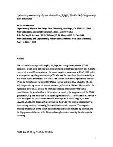
2. The basic structure The NbSe3 room-temperature (RT) basic structure [11] is shown in figure 1. It is constructed from three types of symmetry-related pairs of bi-capped trigonal prismatic (BCTP) columns. These columns are formed of Nb chains in Se cages, aligned parallel to the monoclinic b0-direction. The inter-column covalent bonding forms corrugated layers parallel to the b0-c0 monoclinic plane, separated by van der Waals (vdW) gaps. Thus, the structure is strongly anisotropic in all three dimensions: in addition to the 1-D nature characterized by the BCTP columns, it also shows a pronounced twodimensional character, whose origin is in the covalently bonded layers. Among the three different types of BCTP columns in NbSe3 the type-I and type-III columns are rather similar, with one short Se-Se distance forming the equilateral bases of the prisms, while the bridging type-II columns appear more regular, with almost isosceles-like bases. 3. The CDW models It was argued from the very beginning [12] that two incommensurate (IC) CDWs appear independently at different onset temperatures along two of the three available BCTP columns: one with wave vector q1 = (0,0.241,0) below T1 = 144 K appearing along type-III columns and a second with wave vector q2 = (0.5,0.260,0.5) below T2 = 59 K appearing along type-I columns. This generally accepted perception of CDW formation and ordering appeared to be in good accord with a variety of experiments performed on NbSe3: in addition to the nonlinear transport properties attributed to CDW sliding and pinning [13-27], there were also electron [28] and x-ray diffraction studies [29-32], nuclear magnetic resonance (NMR) [33-35] and angular resolved photoemission spectroscopy [36,37] performed. Figure 1 (Color online) The structure However, the model seems to be in disaccord with some of NbSe3 [11]. The red (dark), orange transmission electron microscopy (TEM) results [38] (gray) and yellow (light) balls and particularly with the latest LT STM observations represent Se atoms along type-II, type[39-42]. These difficulties are not to be ignored, not only I and type-III bi-capped trigonal because of the exceptional resolution achieved in the LT prismatic cages with the 8-coordinated STM experiments, but also because of the very localized small black (dark) balls representing structural information this method is able to supply. Nb atoms. (b) The marked detail with It was suggested later in an alternative model the shortest Nb-Se bonds indicated by [43] that both IC CDWs are formed simultaneously and red (dark) lines. statistically along type-I columns below T1 and in addition along type-III columns below T2. According to this model the two CDWs are supposed to be separated into highly anisotropic and unstable layered nano-domains, oriented parallel to the vdW gaps. This model is based on two conditions: first, the domains must be sufficiently small to extinguish in the diffraction experiments the q2 contribution to the reciprocal space between T1 and T2 and second, the domains must be in proper phase relationships. The first condition requires short correlation lengths of both domain types in comparison with the instrumental coherence regions, while the second requirement depends on the absolute values of the two q-vectors.
2
4. The experimental evidence The available models for CDW ordering in NbSe3 are to be evaluated on the basis of the following relevant experimental evidence. X-ray and electron diffraction: Tsutsumi et al. [28] first reported observation of diffuse precursor scattering in electron diffraction patterns of NbSe3 at temperatures above the q1 CDW transition. Next, several x-ray analyses were performed on both, the q1 and q2 satellites. By measuring the line widths of both types of CDW satellites Fleming, Moncton and McWhan [29] found an anisotropy ratio of an order of 5 between the correlation lengths ξb* and ξa*, i.e. parallel to the chains and perpendicular to the cleavage planes. The estimated parallel values a few degrees above T1 and T2 were ξb* > 5 nm (measured on a q1 satellite at 160 K) and ξb* > 10 nm (measured on a q2 satellite at 62 K), while the corresponding perpendicular values were ξa* ≈ 1.2 nm and ξa* ≈ 3 nm. Moudden et al. [30] determined after proper deconvolutions of the scattering profiles for the q1 satellites a resolution limited correlation length ξb* > 280 nm at 80 K (i.e. bellow T1) and ξb* ≈ 70 nm at 155 K for scans along b0* and ξa* ≈ 4.2 nm, ξb* ≈ 14 nm and ξc* ≈ 0.5 nm for the transverse scans along a0* at about 6 K above T1. They also reported a slight variation of the q1 vector between T1 and 80 K. Rousière et al. [31] performed x-ray measurements of the pretransitional structural fluctuations for both, q1 and q2 satellites. They found at 72 K a smaller anisotropy for the q2 satellites (1:3.5:6) as compared to the one of the q1 satellites (1:4:20), with the ratios given along the perpendicular b0, a0, and c0* directions, respectively. The intrachain correlation lengths ξb and the interchain ξa values were found to be a few degrees above the transition temperatures for both CDW wave vectors similar, while the corresponding ξc* values were at larger variance. Approximate values for the q2 satellites at 65 K (deduced from [31]) are ξb ≈ 6.5 nm, ξa ≈ 2 nm and ξc* ≈ 1.5 nm. Such correlation lengths, particularly those measured perpendicular to the chains, indeed appear short in comparison with the coherence regions, whose estimated sizes for synchrotron x-rays radiation extend 125 nm [44] and for highenergy electrons in conventional TEM experiments 380 nm [45]. A structural analysis of the modulated structure was performed with synchrotron radiation [32]. The atomic displacements along the three BCTP columns were found to be in accord with the original Wilson´s model. However, if segments of variable lengths along the type-III (below T1) and in addition along the type-I columns (below T2) are modulated alternatively by the q1 and q2 wave vectors, as suggested in the domain model, the overall contribution to the reciprocal space would in fact appear identical for both suggested models. The same arguments also apply for any high energy electron diffraction experiments. Thus, if a disorder on a nanoscale indeed takes place in NbSe3, both models cannot be distinguished on the basis of the corresponding diffraction experiments. NMR: NMR measurements were performed at room temperature (RT), 77 K (LNT) and 4.2 K (LHeT) on powdered samples and on samples made of a large number of properly aligned crystals [33-35]. The 93Nb (I=9/2) spectra recorded at RT with the magnetic field parallel to the crystallographic b0 direction resolved 27 lines, which clearly corresponded to the three different Nb sites. While one set of lines remained unchanged on cooling to the LHeT, one of the remaining two sets of lines became smeared at LNT and the remaining set in addition at LHeT. This behavior is indeed in accord with the original model [12], where the Nb sites of the type-II columns are not supposed to be affected by the CDW formation, while the q1 CDW is expected to appear on cooling below T1 along the type-III columns and in addition the q2 CDW below T2 along the remaining type-I columns. However, the behavior is also in accord with the domain model [43]; the problem with NMR is that the IC nature of the two CDWs clearly reveals contributions from different types of columns, but does not distinguish the corresponding Nb sites with regard to q1 and q2. TEM: In addition to the early high-energy electron diffraction studies [28] NbSe3 was also investigated by satellite dark field TEM [38]. Elongated strands, in average 20 nm wide and 2000 nm long, crossed by unstable Moiré-like fringes with spacings from only 8 nm to a few 100 nm, were observed in samples cooled to temperatures both above and below T2. The strands and fringes were observed in addition to other contrast effects, which altogether exhibited a characteristic unstable “twinkling”. The appearance of these features above T2 could not be properly explained on basis of the original Wilson's model. Thus, the described TEM experiments were the first indication that the observed instabilities might be inconsistent with the generally accepted model.
3
LT STM: In spite of their high resolution the recently published LT STM images of NbSe3 [40-42] are difficult to interpret. The main problem represents the variation of the images with the tunneling parameters, which vary the detected CDWs, particularly their intensities. In addition, subsurface effects are regularly detected superimposed onto the surface contribution, which complicates the interpretation. Nevertheless, there are a few details, some in accord with both models (points 1. to 3.), while the rest seem to support a modified domain model: 1. Dependent on temperature, all images shown reveal either only one (type-III) or two (typeIII and type-I) strongly modulated BCTP columns along the basic structure unit cell periodicity c0. 2. The intensity of the CDWs recorded varies largely with the tunneling parameters, particularly with a switched polarity of the applied gap voltage. 3. The strongly modulated columns are along the c0 direction ordered either in-phase (if there is only one strongly modulated column per c0) or out-of-phase (if these appear in pairs). In the second case the adjacent pairs as units are also ordered out-of-phase, which automatically enlarges the lateral periodicity into 2c0. 4. All strongly modulated surface columns show within the well ordered regions the same CDW periodicity along the columns. 5. Regardless of the actual labeling of the columns, there is always one mode present (either as a strong surface modulation or as a superimposed weak contribution from bellow the surface), whose ordering enlarges the lateral periodicity into 2c0. While the observation described under point 4. clearly supports the suggested domain model, the one described under point 5. raises doubts about this model as well. In this context it is also interesting to reinvestigate the first of the published LT STM studies on NbSe3, not only because it triggered at the time it was published a discussion about its interpretation [39], but also because it shows the best resolution and thus supplies some key evidence for the evaluation of the models. The image reveals pairs of strongly modulated chains along c0. These are both modulated by the same CDW and ordered out-of-phase, as described under point 3. above. With the lateral periodicity enlarged into 2c0, the two adjacent columns forming pairs can only represent type-III and type-I columns, both modulated by the same q2 CDW. This is clearly in support of the domain model. What seems to be in disaccord with it are the remaining single weakly modulated columns. According to their position and intensity they obviously represent subsurface columns, which form pairs with the adjacent strongly modulated surface columns. The modulation periodicity along these columns appears slightly larger as compared to the one along the strongly modulated surface columns with an in-phase ordering along c0. Thus, they seem to represent the alternative q1 CDWs. According to their position along c0 the adjacent surface-subsurface pairs can only represent the type-I pairs of columns; the type-III subsurface columns are positioned bellow their surface counterparts and cannot be detected. All columns show in addition to the modulation also an atomic resolution, however only one chain per column. This is in accord with expectations in case of the type-III and type-I columns, whose trigonal prismatic bases are equilateral with one short Se-Se bond, but is somewhat surprising in case of the remaining unmodulated chains. In accord with their position these show the surface type-II columns, whose trigonal prismatic bases are almost isosceles. Although these details are in accord with the basic supposition of the domain model, i.e. the existence of layered domains with both type-III and type-I columns modulated by either of the two CDWs, they are in disaccord with its prediction that the same CDWs appear along strongly bonded pairs of column. The described details rather indicate that the strongly bonded layers are composed of q1 and q2 sublayers, whose interchanging results in the domain structure. 5. Discussion LT STM is of particular importance, because the method is basically different from the alternative methods, such as NMR, electron spin resonance, various diffraction methods, and last but not least even high-resolution TEM. Although these approaches are beyond any doubt capable of achieving resolution on an atomic scale, the scanning probe microscopies, and STM in particular, are the only methods where information is not collected statistically over a relatively large sample. STM has also drawbacks; it is a surface sensitive method and the interaction between the scanning tip and the surface may be sufficiently strong to induce changes in the surface. But in spite of that, it is certainly capable of revealing details like nano-domains, which might due to their small sizes and
4
averaging within experimental coherence regions be overlooked by all methods based on statistics, regardless of their high resolution. This by no means reduces the importance of the alternative methods, but rather requires a comparison of all results, which should together lead to a single acceptable conclusion. Next, there is the question of the STM image formation and its interpretation. Due to the Fermi surface shape, the major contribution to the surface density of states in NbSe3 is supposed to come from the corrugated top Se layer [41]. However, it should be taken into account that a charge distribution can also be detected over larger distances and may show details located below the surface. Such effects, attributed to a charge transfer to the surface have been observed before, e.g. in the superstructures formed by intercalated metal atoms in the subsurface vdW gaps of NbS2 and NbSe2 [46] and in the case of unstable domain boundaries formed along such gaps in the monoclinic NbTe2 [47]. The observed long-range ordering in NbSe3 [41] must be of a similar origin, as schematically shown in figure 2a. A periodicity of 116 b0 is chosen along both columns, with the first half (i.e. 58 b0, the LP that accommodates 14 q1 and 15 q2 CDW modulation periods [43]) of the top column modulated with q2 and the second half with q1, while the column beneath is modulated in the opposite sense. If the charge modulations along two of such adjacent columns are indeed detected together, characteristic beating should be observed in the STM images. If in addition the q2 sections are statistically displaced by half shorter q1 sections (7 q1 periods extending over 29 b0 only [30]), as shown in figure 2b, the close proximity of the two columns would result in a q1 contribution to the reciprocal space only [43]. However, the q2 sections would still Figure 2 A model of a possible combined be detected by STM. q1 and q2 modulation along two adjacent All details revealed by LT STM, together NbSe3 type-III columns (a). The same after with the results of the alternative methods, are in the q2 part was displaced along the lower accord with a partly modified domain model. column by π (b). According to this, q1 and q2 CDW segments can be interchanged along the type-III columns bellow T1 and in addition along type-I columns bellow T2. The suggested disorder explains the appearance of the CDW domain structure and the characteristic twinkling in the satellite dark field TEM images. The type-II columns remain more or less unmodulated in the entire temperature range between RT and LHeT. Since the type-III pairs of columns form slabs parallel to the a0-b0 plane, the CDW ordering between T1 and T2 also takes place along these slabs. However, contrary to the predictions of the original domain model [43] the LT STM results suggest that the strongly bonded pairs of columns are alternatively modulated by the q1 and q2 CDWs. Accordingly, layered domains of modulated BCTP columns are formed parallel to the b-c plane and composed of at least a pair of adjacent q1 and q2 sublayers, which can easily be interchanged as part of the unstable domain structure. The four modes present bellow T2, i.e. q1 and q2 along both type-III and type-I columns, can under certain conditions be replaced by two only. These require that they appear as coupled pairs, whose composed LP commensurate modulation fits to 58 b0 and stretches laterally across a pair of columns (either type-III or type-I). The IC components of the two wave vectors must in that case add to ½ exactly, which is due to one report [44] and due to a slight variation of the q1 vector with temperature [30] still not proved beyond any doubt. It appears that the origin of the peculiar CDW ordering in NbSe3 and the structurally related compounds is in its basic structure, composed of symmetry related pairs of BCTP columns, which are
5
alternatively modulated by the two q vectors. The rest depends on possible ordering of such units into anisotropic nano-domains with the peculiar contribution to the reciprocal space. The suggested CDW modulated structure in NbSe3 is in accord with the available experimental evidence and particularly with all details revealed by LT STM and the corresponding Fourier transforms [39,41] and is not in contradiction with the recently reported surface dependence of the T2 transition temperature [42]. 6. Conclusions The details revealed by the LT STM studies raise questions regarding a number of aspects of the conventional picture of the CDW states occurring in NbSe3. The available experimental evidence supports a revised alternative model, based on the existence of coupled layered q1 and q2 nano-domains. The suggested model brings into accord all important details revealed in the LT STM experiments, like the confinement of the modulation to certain structural segments, the modulation periodicity and its phase relationship with the neighboring columns, and can be brought into accord with the results of a few alternative methods (x-ray, NMR and TEM), which are based on a statistical collection of data. Further experimental and theoretical studies are needed to clarify these results further and particularly to advance our understanding of the physical reasons for the unique phenomenon in solid state science.
Acknowledgements Financial support of the Slovenian Research Agency (ARRS) (AP, HJPvM, RŽ and EZ) and of the Natural Sciences and Engineering Research Council of Canada (JCB) is gratefully acknowledged.
References: [1] Thompson A H, Zettl A and Grüner G 1981 Phys. Rev. Lett. 47 64 [2] Zettl A, Jackson C M, Janossy A, Grüner G, Jacobsen A and Thompson A H 1982 Sol. St. Comm. 43 345 [3] Wang Z Z, Saint-Lager M C, Monceau P, Renard M, Gressier P, Meerschaut A, Guemas L and Rouxel J 1983 Sol. St. Comm. 46 325 [4] Wang Z Z, Monceau P, Renard M, Gressier P, Guemas L and Meerschaut A 1983 Sol. St. Comm. 47 439 [5] Dumas J, Schlenker C, Marcus J and Buder R 1983 Phys. Rev. Lett. 50, 757 [6] Pouget J P, Kagoshima S, Schlenker C and Marcus J 1983 J. Phys. (Paris) Lett. 44 L113 [7] Ganne M, Boumaza A, Dion M and Dumas J 1985 Mat. Res. Bull. 20 1297 [8] Collins B T, Ramanujachary K V and M. Greenblat 1985 Sol. St. Comm. 56 1023 [9] Lacoe R C, Schulz H J, Jérome D, Bechgaard K and Johannsen I 1985 Phys. Rev. Lett. 55 2351 [10] Billinge S J L 2010 http://physics.aps.org/articles/v3/25 Cliffe M J, Dove M T, Drabold D A and Goodwin A L 2010 Phys. Rev. Lett. 104 125501 [11] Hodeau J L, Marezio M, Roncan C, Ayroles R, Meerschaut A, Rouxel J and Monceau P 1978 J. Phys. C: Solid State Phys. 11 4117 [12] Wilson J A 1979 Phys. Rev. B 19 6456 [13] Ong N P and Monceau P 1977 Phys. Rev. B 16 3443 [14] Grüner G 1994 Density Waves in Solids, Addison-Wesley, Reading [15] Monceau P, Ong N P, Portis A M, Merschaut A and Rouxel J. 1976 Phys. Rev. Lett. 37 602 [16] Fleming R M and Grimes C C Phys. Rev. Lett. 1979 42 1423 [17] Monceau P. 1985 Electronic Properties of Inorganic Quasi-One-Dimensional Matals, Part II, ed Monceau P, D. Reidel, Dordrecht p. 139.
6
[18] Withers R L and Wilson J A. 1986 J. Phys. C 19 4809 [19] Ayari A, Danneau R, Requardt H, Ortega L, Lorenzo J E, Monceau P, Currat R, Brazovskii S and Grübel G 2004 Phys. Rev. Lett. 93 106404 [20] Hor Y S, Xiao Z L, Welp U, Ito Y, Mitchell J F, Cook R E, Kwok W K and Crabtree G W 2005 Nano Letters 5 397 [21] Physics and Chemistry of Low-Dimensional Inorganic Conductors, eds Schlenker C, Dumas J, Greenblatt M and van Smaalen S 1996 354 NATO Advanced Studies Institute Series B: Physics, Plenum, NY [22] Proceedings of the International Workshop on Electronic Crystals (ECRYS 2008) 2009 Cargèse, France, 2008: Physica B 404 (3-4) [23] Thorne R E 1992 Phys. Rev. B 45 5804 [24] Danneau R, Ayari A, Rideau D, Requardt H, Lorenzo J E, Ortega L, Monceau P, Currat R and Grübel G 2002 Phys. Rev. Lett. 89 106404 [25] Slot E, van der Zant H S J, O'Neill K and Thorne R E 2004 Phys. Rev. B 69 073105 [26] O'Neill K, Slot E, Thorne R E and van der Zant H S J 2006 Phys. Rev. Lett. 96 096402 [27] Isakovic A F, Evans P G, Kmetko J, Cicak K, Cai Z, Lai B, and Thorne R E 2006 Phys. Rev. Lett. 96 046401 [28] Tsutsumi K, Takagaki T, Yamamoto M, Shiozaki Y, Ido M, Sambongi T, Yamaya K and Abe Y 1977 Phys. Rev. Lett. 39 1675 [29] Fleming R M, Moncton D E and Mc Whan D B 1978 Phys. Rev. B 18 5560 [30] Moudden A H, Axe J D, Monceau P and Lévy F 1990 Phys. Rev. Lett. 65 223 [31] Rouzière S, Ravy S, Pouget J P and Thorne R E 1996 Solid State Comm. 97 1073 [32] van Smaalen S, de Boer J L, Meetsma A, Graafsma H, Sheu H-S, Darovskikh A, Coppens P and Lévy F 1992 Phys. Rev. B 45 3103 [33] Devreux F 1982 J. Phys. (Paris) 43 148 [34] Ross Jr J H, Wang Z and Slichter C P 1986 Phys. Rev. Lett. 56 663 [35] Suh S, Clark W G, Monceau P, Thorne R E and Brown S E 2008 Phys. Rev. Lett. 101 136407 [36] Schäfer J, Rotenberg Eli, Kevan S D, Blaha P, Claessen R and Thorne R E 2001 Phys. Rev. Lett. 87 196403 [37] Schäfer J, Sing M, Claessen R, Rotenberg Eli, Zhou X J, Thorne R E and Kevan S D 2003 Phys. Rev. Lett. 91 066401 [38] Fung K K and Steeds J W 1980 Phys. Rev. Lett. 45 1696 [39] Dai Z, Slough C G and Coleman R V 1991 Phys. Rev. Lett. 66, 1318 van Smaalen S, De Boer J L, Coppens P and Graafsma H 1991 Phys. Rev. Lett. 67 1471 Dai Z, Slough C G and Coleman R V 1991 Phys. Rev. Lett. 67 1472 [40] Brun C, Wang Z Z and Monceau P 2005 J. Phys. IV (France) 131 225 [41] Brun C, Wang Z Z and Monceau P 2009 Phys. Rev. B 80 045423 [42] Brun C, Wang Z Z, Monceau P and Brazovskii S 2010 arXiv:1002.4767v1 [condmat.mes-hall] [43] Prodan A, Jug N, van Midden H J P, Böhm H, Boswell F W and Bennett J C 2001 Phys. Rev. B 64 115423 [44] Fleming R M, Chen C H and Moncton D E 1983 J. de Phys. (Paris) 44, C3-1651 [45] Lüth H 1995 Surfaces and Interfaces of Solid Materials, Springer, Berlin p. 207 [46] Prodan A, Marinković V, Rojšek M, Jug N, van Midden H J P, Boswell F W, Bennett J C and H. Böhm, 2001 Surf. Sci. 476/1-2 71 [47] Cukjati D, Prodan A, Jug N, van Midden H J P, Hla S W, Böhm H, Boswell F W and Bennett J C 2002 phys. stat. sol. (a) 193 246
7