Correlation of Experimental and Simulated Cure-Induced Photoresist Distortions in Double Patterning Thomas I. Wallow*a, Mahidhar Rayasama, Masanori Yamaguchib, Yohei Yamadab, Karen Petrilloc, Kenji Yoshimotod, Jongwook Kyea, Ryoung-han Kime, and Harry J. Levinsona a GlobalFoundries, 1050 East Arques Avenue, Sunnyvale, CA 94085; b Ushio Incorporated, 1194 Sazuchi, Bessho-cho, Himeji, Hyogo Prefecture JAPAN 6710224; c IBM Corporation, 255 Fuller Road, Albany, NY, 12203; d GlobalFoundries, 2070 Route 52, Hopewell Junction, NY, 12533; e GlobalFoundries, 255 Fuller Road, Albany, NY, 12203 ABSTRACT Numerous alternate processes are under industry-wide evaluation as simplifications to current double patterning methods. Reduction in process complexity and cost may be achieved by use of photoresist stabilization methods that eliminate one etch step by allowing a second resist to be patterned over the first resist pattern. Examples of stabilization methods using numerous curing processes have been reported. At least some resist shrinkage during stabilization appears to be generally observed for these methods. We evaluate the link between volumetric shrinkage and threedimensional pattern distortion for a variety of resist geometries using experimental and simulation-based methods. Experimental resists designed for double patterning using 172 nm UV resist curing were evaluated and showed shrinkage of less than 10 percent. Several simplified metrology approaches for measuring shrinkage as well as inferring shrinkage distortions were assessed. For top-down SEM measurements, elbow inner corner rounding measurements appear to be a usefully robust method for estimating shrinkage distortion. Finite element analysis of resist structures yields shrinkage distortions that are in good qualitative and quantitative agreement with experiments, and thus appears to provide a provisionally general and useful method for predicting pattern distortions that arise during cure-based resist stabilization methods used in double imaging. Keywords: photoresist, distortion, shrinkage, curing, double patterning, simulation, metrology, 172 nm
1. INTRODUCTION Double patterning methods that simplify integration of lithographic and etch processes are of growing importance due to their potential for improved manufacturing throughput and cost savings. Increasing efforts in this area center on double imaging processes in which two or more independent lithographic patterns are generated in sequentially applied resist films, then transferred in a single etch step.1-14 In previous reports,15,16 we demonstrated that 172 nm cure stabilization, when properly implemented, can result in superior retention of photoresist profiles compared to broadband UV curing (Fig. 1). We documented that the approximately 25 percent volumetric shrinkage observed for a non-optimized resist during stabilization resulted in controlled CD trimming and thickness loss as well as three-dimensional resist pattern distortions that included a) lineend tilting and pullback and b) elbow corner tilting and displacement. We concluded that shrinkage control during any stabilizing process is a critical factor for both a) determining the suitability of a given double imaging method for patterning complex resist structures and b) designing photoresists for cure-based double imaging methods.
*
[email protected]; 408-749-2513 Advances in Resist Materials and Processing Technology XXVI, edited by Clifford L. Henderson, Proc. of SPIE Vol. 7273, 727309 · © 2009 SPIE · CCC code: 0277-786X/09/$18 · doi: 10.1117/12.814474
Proc. of SPIE Vol. 7273 727309-1
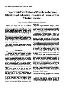
a)
Pattern Freeze I 72nm Flood
w I
St
Pattern
Coat
w
I'll' Iran tIer
I
I
Cure Bake
LaL 250 Develop
b)_
: iii 1° Pattern
172 nm Freeze
Cross-Grid Pattern 96 nm pitch
Fig. 1. a) Schematic of double patterning using 172 nm resist stabilization. b) Example of double patterning using an experimental immersion-compatible photoresist to pattern cross-grid contact holes on a 96 nm pitch.
In this study, we expand our previous explorations of the link between cure shrinkage and three-dimensional pattern distortion effects. Additionally, we characterize shrinkage of experimental photoresists designed for optimal 172 nm stabilization. These resists show greatly reduced shrinkage and distortion relative to previously studied resists. In order to characterize distortions using straightforward top-down SEM measurements, we evaluate several approaches, using finite element analysis (FEA) simulations to guide our experimental methods. The predictive success of FEA indicates that it continues to be a powerful and straightforward tool for evaluating the impact of cure shrinkage on double imaging processes. Ultimately, FEA may play a useful role in understanding lithographic design rule tolerance for photoresist shrinkage distortions.
2. EXPERIMENTAL Patterning evaluations were conducted using immersion scanners at 1.2 and 1.35 NA. Following processing, wafers were transported in standard carriers to the 172 nm cure processing facility. The 172 nm cure chamber was designed for highly reproducible irradiation. It allows process evaluation and development under controlled environmental conditions and is configured with in-situ monitoring probes to achieve uniform process conditions. All wafer handling was carried out in an R&D cleanroom. Several experimental and commercial 193 nm resists were chosen as the focus of these studies based on preliminary screening. We note that response to pattern freezing steps varies widely among experimental and commercial resists. Films were coated at 135 nm nominal thickness on a reflectivity-optimized commercial BARC. All standard process steps used supplier-recommended conditions. Standard CD-SEMs and commercial analytical SEMs were used for capturing images for pattern deformation studies. Image analysis was conducted using SuMMIT software. Corner rounding measurements using SuMMIT used a fitting algorithm that estimates corner radius using a ‘missing area’ fit to an ideal 90o corner.17
Proc. of SPIE Vol. 7273 727309-2
Finite element analysis employed ANSYS software18 and followed a methodology that was inspired by Colburn et al., who characterized interactions between densification, mechanical properties and aspect ratio for lithographic photopolymers.19 Details of the simulation approach have been described in a previous report.16
3.
RESULTS AND DISCUSSION
3.1 Shrinkage during resist stabilization Fig. 2a illustrates the experimental correlation between 172 nm cure dose and volumetric shrinkage as measured using offsets between dose-linearity curves of uncured and cured resist patterns. In calculating volumetric shrinkage from ΔCD, isotropic shrinkage is approximated as shown in Fig. 2b: experimentally measured ΔCD is assumed to be accompanied by Δh, which is related to ΔCD by the initial feature aspect ratio hi/CDi (i. e., Δh = ΔCD*(hi/CDi)). In the absence of reflow effects, this approximation is reasonable based on previous work.
65
62.5 -
a)
Resist B
Line Shrinkage
60 -
b)
57.5 -
52.5 50 - -
control
.1000 mJ/cm2
47.5 --
1000 mJ/cm2 *105 CS
45
09
0.95
1
1.05
11
Normalized 193nm dose Fig. 2. a) Shrinkage for experimental resist ‘B’ during stabilization. No shrinkage is detectable from 172 nm irradiation at 1000 mJ/cm2. If a post-UV bake at 165 oC is applied, approximately 2.5 nm of line slimming is observed for a nominal 55 nm CD target structure. b) Schematic of volumetric shrinkage estimation method.
Volumetric shrinkage was inferred for two experimental photoresists designed for 172 nm stabilization using this method. Fig. 3 summarizes results for both resists. For relevant process conditions, both resists show shrinkage associated with stabilization of less than 10 percent, which is a marked improvement over the shrinkage behavior of a previously studied resist that was not designed for 172 nm stabilization. With process optimization, shrinkage of less than 5 percent appears possible. Some differences between the two resists are apparent. Resist ‘B’ shows almost no shrinkage following 172 nm irradiation, but shows modest bake-temperature-dependent shrinkage if a post-UV bake is applied. Resist ‘C’ shows modest shrinkage for both process steps. In addition, resist ‘C’ appears susceptible to reflow if high 172 nm doses and bake temperatures above 150 oC are used. Since lower doses and temperatures are sufficient to stabilize resist ‘C’, this observation does not represent a significant practical limit on process parameters. Low shrinkage materials will enable less restricted double patterning applications. For the 5-10 percent shrinkage seen using resist ‘B’ and ‘C’, previous FEA results suggest that metrics for corner tilt distortion (d(COM); fig. 4a) and linedistortion (d(LE)) will be reduced to less than 10% of CD for features stabilized using the 172 nm process.16
Proc. of SPIE Vol. 7273 727309-3
a)
66
I 72 nm only
626 60
25
67.6
66 62.6
20
E so
0)
-
5476 46
06
066
=
I 06
-i
IS
(I)
66
o 10
626
a)
60
Es S
67.6
0
66
>
62.6
0
60
500
0
o4J2 66bb
47.6 46
06
0.66
1000
1500
172nm Dose (mJ/cm2) I
II
1.06
Normalized 193 nm dose
b)
76
72.6 -
-
70
25
67.6 66
.1250006 .1500006
0)
60
0
E 67.6
.E IS
See 6
0
(Reflow?)
No Bake
p 20
62.6
0.6
=
I 06
0.66
(I)
o 10
72.6 70
a)
J 67.6
E S
0
66
>
62.6
0
60
0
67.6
500
1000
I 500
172nm Dose (mJ/cm2)
66
0.6
0.6
0.66
I
106
1.1
1.16
Normalized 193 nm dose
Fig. 3. a) Shrinkage estimates for a variety of stabilization conditions for resist ‘B’. b) Shrinkage estimates for a variety of stabilization conditions for resist ‘C’.
3.2 Improved shrinkage characterization metrology Previous attempts at characterizing shrinkage distortions have ultimately required time-consuming and non-automatable SEM methods.15,16,20 Simpler automated methods are desirable for process development, optimization, and monitoring. Here, we focus first on the elbow corner displacement effects before considering new approaches. Fig. 4a reviews the effect of shrinkage on elbow corners. Shrinkage in the elbow arms exerts stresses at the elbow that tilt it inward, producing an effective displacement of the corner position that may be characterized by d(COM), the distance the corner moves from its initial position at its cross-sectional center of mass along diagonal cut line ii. Tilt SEM allows measurement of the tilt angle, which in turn allows d(COM) to be estimated with some confidence.16 Examination top-down SEM images of features that were known to be distorted proved challenging at first. However, consideration of a ‘worst-case’ scenario allowed us to refine our methods. Figs. 4b and 4c compare elbow corners before and after a reflow bake, which can result from a poor choice of stabilizing process conditions.15 Note the extreme elbow tilt and displacement apparent in Fig. 4c. Measurements of the corresponding top-down SEM images revealed that attempts to infer changes in corner position from extrapolation of inner and outer arm edges before and after reflow yielded unreliable results. In contrast, we found that measurement of the inner corner radius was reproducible and that the measured radius increased by nearly 20 percent following reflow. Note that measurement of the inner corner radius cleanly reflects the resist-top profile along the feature. Measurement of the corresponding outer corner radius is complicated by the sloped outer elbow sidewall, and gives results that are much less straightforward to interpret.
Proc. of SPIE Vol. 7273 727309-4
a)J
Corner Displacement (Cut (ii))
25% Shrinkage Simulation
Fig. 4. Elbow corner distortion due to shrinkage and reflow effects. a) Illustration of elbow shrinkage distortions along diagonal cut-line ii. Corners are tilted inward resulting in displacement. The D(COM) metric defines the center of mass displacement of the distorted corner. b) Tilt- and top-down SEM views of elbows before reflow distortion. c) Tiltand top-down SEM views of elbows after reflow distortion. Growth of inner elbow radius is clearly detectable under reflow conditions.
FEA simulations show similar inner corner distortions. Fig. 5 illustrates the relationships between both shrinkage and resist aspect ratio (aspect ratio is defined for arm beams removed from the corner- see cutline i in Fig. 4a) and inner corner radius growth.
J.S
AR
AR =
1.15 (I)
5% Shrinkage
=
1.125 -
- 10% Shrinkage
15% Shrinkage
U)
1.1
o 1.075
w
N
0
1.05
U)
z0
1.025
15
1.75
2
2.25
2.5 2.75
3
3.25
Aspect Ratio (h/w) Fig. 5. FEA simulation of inner corner rounding. Increases in shrinkage and feature aspect ratio are directly correlated with an increase in inner corner radius.
Proc. of SPIE Vol. 7273 727309-5
We next examined isolated elbow structures patterned in resist ‘B’ and resist ‘C’ (Nominal elbow arm CD is 50 nm at 135 nm film thickness with ideal aspect ratio ~2.7. The real aspect ratio is somewhat smaller due to 10-20 nm resist top loss during development.) Fig. 6 shows that inner corner rounding of elbows before stabilization is independent of imaging dose, but increases systematically with imaging dose following 172 nm processing for both resists. We attribute these results to aspect-ratio dependent shrinkage distortion as illustrated in Fig. 5: as imaging dose increases, resist aspect ratio also increases, which results in larger corner radii following shrinkage distortion. The 5-10 percent shrinkage estimated from exposure latitude offsets (Fig. 3) should yield an approximately 5-7 percent increase in inner corner radius at aspect ratio ~2.5 based on FEA simulation, assuming that no reflow occurs. Corner radius growth for resist ‘B’ varies with imaging dose, but is near 5-10 percent at CD = 50 nm (normalized 193 nm dose = 1), which is in good agreement with simulation given uncertainties associated with modest resist top loss during development. The conditions chosen for resist ‘C’ are near the onset of slight reflow- note that growth of the inner radius is somewhat larger than for resist ‘B’. Additionally, there appears to be inner radius growth in the absence of 150 oC bake under high 172 nm dose conditions for resist ‘C’. This observation is not currently understood and requires further characterization.
Resist B
Resist C
145
145 Control
E 140
l000mJ/cm2
140
1OOOmJ/cn2+165Cb
135
135
130
130
125
125
120
120
o 115
115
110
110
Control
0
09
095
105
11
-1000 mJ/c*n2
1Ofl rJn215OC
085
0.9
0.95
05
1.1
1.15
Normalized 193 nm Dose Fig. 6. Inner corner rounding measured in resist ‘B’ and resist ‘C’ for a nominal 50 nm isolated elbow.
Finite element analysis can also be used to identify other potentially useful shrinkage distortion metrology targets. Given the relatively noisy data produced by measurement of inner corner radii, we focused on targets that would allow simple analysis image capture and analysis of multiple features. Contact holes patterned on asymmetric x and y pitches appear to be a useful target. Fig. 7 summarizes simulations of elliptical deformation that results from shrinkage. Contact axis ratio is predicted to grow both as shrinkage increases and as x and y pitches become more asymmetric. Given that analysis of large numbers of contact holes is straightforward, it may be possible to assess deformation in these target patterns with greater accuracy. Comparison with experimental results is underway and will be presented in another study.
Proc. of SPIE Vol. 7273 727309-6
1.125 .5% Shrinkage
.2
Contact h/d = 2.5
10% Shrinkage 15% Shrinkage
1.1
.20% Shrinkage
w 1.075
1.025
0
2
4
6
x/y Pitch Ratio Fig. 7. Contact hole shrinkage distortions. Asymmetric pitches produce elliptically distorted contacts following shrinkage.
4. CONCLUSION In instances where resist shrinkage occurs during stabilizing treatments for double patterning, shrinkage-related distortions can be observed and predicted. In this study, we have expanded characterization of shrinkage distortion to new resists that are ‘designed for freezing’ using 172 nm cure stabilization. We find that these resists show much lower shrinkage (less than 10 percent) and shrinkage distortions in the 172 nm process than materials studied earlier, and perform well in sub-45 nm logic node immersion lithography. Metrology challenges remain for characterizing distortions using top-down SEM. However, we have shown that elbow corner rounding measurements hold promise for inferring shrinkage and accompanying distortions, and are in reasonable quantitative agreement with both experimental shrinkage estimates based on exposure latitude curve offsets and FEA simulation. Additionally, we report on simulations that suggest that other test structures, such as contact holes patterned on asymmetric x and y pitches, may be even more sensitive monitors for shrinkage distortions.
5. ACKNOWLEDGMENTS We are grateful to Hoa Truong and Bob Allen (IBM Almaden Research Center) for assistance with tilt-SEM images. We would also like to thank Hiroshi Sugahara (Ushio Incorporated) for assistance with thin film characterization and Toru Fujinami (Ushio America) for many helpful discussions. Finally, we would like to thank resist suppliers for their development efforts in support of this double patterning approach.
REFERENCES [1] [2] [3] [4]
[5]
Nakamura, H.; Onishi, Y.; Sato, K.; Tanaka, S.; Mimotogi, S.; Hashimoto, K.; Inoue, S., “Contact Hole Formation by Multiple Exposure Technique in Ultra-low k1 Lithography,” Proc. SPIE 5377, 225, (2004). Nakamura, H.; Onishi, Y.; Sato, K.; Tanaka, S.; Mimotogi, S.; Hashimoto, K.; Inoue, S., “Contact hole formation by multiple exposure technique in ultra-low k1 lithography,” JM3 4, 023005, (2005). Owe-Yang, D.-C.; Yu, S.; Chen, H.; Chang, C.; Ho, B.; Lin, J.; Lin, B., “Double Exposure for the Contact Layer of the 65-nm Node,” Proc. SPIE 5753, 171, (2005). Nakamura, H.; Omura, M.; Yamashita, S.; Taniguchi, Y.; Abe, J.; Tanaka, S.; Inoue, S., “Ultra-low k1 oxide contact hole formation and metal filling using resist contact hole pattern by Double L&S Formation Method,” Proc. SPIE 6250, 65201E1, (2007). Nakao, S.; Maejima, S.; Yamamoto, T.; Ono, Y.; Sakai, J.; Yamaguchi, A.; Imai, A.; Hanawa, T.; Sukoh, K., “OPCfree on-grid fine random hole pattern formation utilizing double resist patterning with double RETs,” Proc. SPIE 6250, 153, (2007).
Proc. of SPIE Vol. 7273 727309-7
[6] [7] [8] [9]
[10] [11] [12] [13]
[14] [15] [16] [17] [18] [19]
[20]
Vanleenhove, A.; Van Steenwinckel, D., “A litho-only approach to double patterning,” Proc. SPIE 6250, 65202F1, (2007). Nakamura, H.; Shibata, T.; Rikimaru, K.; Ito, S.; Tanaka, S.; Inoue, S., “Ion implantation as insoluble treatment in resist stacking process,” Proc. SPIE 6923, 692322, (2008). Chen, K.; Huang, W.; Li, W.; Varanasi, P., “Resist freezing process for double-exposure lithography,” Proc. SPIE 6923, 69230G, (2008). Hori, M.; Nagai, T.; Nakamura, A.; Abe, T.; Wakamatsu, G.; Kakizawa, T.; Anno, Y.; Sugiura, M.; Kusumoto, S.; Yamaguchi, Y.; Shimokawa, T., “Sub-40nm half-pitch double patterning with resist freezing process,” Proc. SPIE 6923, 69230H, (2008). Bazin, A.; Pargon, E.; Mellhaoui, X.; Perret, D.; Mortini, B.; Joubert, O., “Impact of HBr and Ar cure plasma treatments on 193nm photoresists,” Proc. SPIE 6923, 692337, (2008). Robertson, S.; Biafore, J.; Graves, T.; Smith, M., “Rigorous physical modeling of a materials-based frequency doubling lithography process,” Proc. SPIE 6923, 6923D1, (2008). Maenhoudt, M.; Gronheid, R.; Stepanenko, N.; Masuda, T.; Vangoidenshoven, D., “Alternative process schemes for double patterning that eliminate the intermediate etch step,” Proc. SPIE 6924, 69240P, (2008). Bekiaris, N.; Cervera, H.; Dai, J.; Kim, R.; Acheta, A.; Wallow, T.; Kye, J. Levinson, H. J.; Nowak, T.; Yu, J, “A Lithographic and Process Assessment of Photoresist Stabilization for Double-Patterning using 172 nm Photoresist Curing,” Proc. SPIE 6923, 692321, (2008). Samarakone, N.; Yick. P.; Zawadzki, M.; Choi, S., “Double printing through the use of ion implantation,” Proc. SPIE 6924, 69242B, (2008). Yamaguchi, M.; Wallow, T.; Yamada, Y.; Kim, R.; Kye, J.; Levinson, H. J., “A Study of Photoresist Pattern Freezing for Double Imaging using 172nm VUV Flood Exposure” J. Photopolym. Sci. Technol. 21, 697, (2008). Wallow, T.; Rayasam, M.; Yamaguchi, M.; Yamada, Y.; Kim, R.; Kye, J.; Levinson, H. J.; “Cure Induced Photoresist Distortions in Double Patterning.” JM3 (2009) (in press). http://www.euvl.com/summit/ http://www.ansys.com/ Colburn, M.; Suez, I.; Choi, B.; Meissi, M.; Bailey, T.; Sreenivasan, S.; Ekerdt, J.; Willson, C. G., “Characterization and modeling of volumetric and mechanical properties for step and flash imprint lithography photopolymers,” J. Vac. Sci. Technol. B 19(6), 2685, (2001). Pollentier, I.; Jaenen, P.; Baerts, C.; Ronse, K., “Sub 50nm gate patterning using line-trimming with 248 or 193 nm lithography,” Future Fab Int. 12, 161, (2002).
Proc. of SPIE Vol. 7273 727309-8