K.E.Kaharudin et al. / International Journal of Engineering and Technology (IJET)
Design and Optimization Approaches in Double Gate Device Architecture K.E.Kaharudin #1, A.H.Hamidon#2, F.Salehuddin #3 #
Centre for Telecommunication Research and Innovation (CeTRI), Faculty of Electronics and Computer Engineering, Universiti Teknikal Malaysia Melaka, Hang Tuah Jaya, Durian Tunggal, 76100 Melaka, Malaysia 1
[email protected] 2
[email protected] 3
[email protected] Abstract—According to Moore’s law, the number of transistor embedded on integrated circuit (IC) doubles approximately every two years. Thus, the size of Metal-Oxide-Semiconductor Field Effect Transistor (MOSFET) has to be scaled down as an increase in packing density. In current technology, the size of a transistor has shrunk below 45nm, and it has already reached its physical limit. Any attempt to shrink the MOSFET beyond this limit will expose MOSFET device to various short channel effects (SCEs) problems. Recently, however, a new architecture of MOSFET known as Double Gate MOSFET has emerged, and this will allow the IC technology continue to be shrunk while sustaining its electrical performance. Several types of Double gate MOSFET are discussed but however, the main focus is to the type of vertical DG-MOSFET. This paper will discuss about the design and optimization approaches in Double-gate (DG) MOSFET device. Keyword- ATHENA, ATLAS, MOSFET, Taguchi, 2k-factorial I. INTRODUCTION The Metal-Oxide Semiconductor Field Effect Transistor (MOSFET) is a main component of various electronics’ applications, especially in integrated circuit (IC) and microprocessor. The transistors contained in a modern microprocessor have reach up to 2.6 billion per chip in the year 2011. MOSFETs are specifically designed for switches in the logic micro-circuit. The combination between n-channel MOSFET and P-channel MOSFET will form complementary metal-oxide-semiconductor (CMOS) and it is widely used in variety of analog circuit such as image sensors, data convertor and radio frequency (RF) circuits. The standard layout of MOSFET simulated by SILVACO ATHENA module is depicted as in Fig 1. The transistor consists of two ntype channel region, which is known as source and drain. These two regions are separated by a region of p-type semiconductor called the substrate [1]. A thin silicon dioxide is growth acts as an insulator to covers the region between source and drain. The insulator is also referred by the name of gate oxide. The same procedures go to p-channel MOSFET but only have been opposite doping materials in source, drain and substrate regions. Fig 2 shows the charge distribution in the structure of n-channel MOSFET device under accumulation, depletion and inversion conditions. Accumulation occurs typically when a low negative voltage is applied to the gate. Therefore, there is a negative charge on the gate attracts holes from the substrate to the oxidesemiconductor interface. Depletion occurs when a low positive voltage is applied to the gate, resulting in some positive charge on the gate. The positive charge on the gate pushes the mobile holes into the substrate, thereby depleting the semiconductor of the mobile carriers and leaving a negative charge in the space-charge region which is due to the ionized acceptor ions. The voltage separating the accumulation and depletion regime is referred to as the flat-band voltage [2]. Inversion occurs when a higher positive potential exceeding critical threshold voltage (VTH) is applied to the gate, thus attracting more positive charge to the gate. The holes are repelled further and small numbers of free electron in the body are attracted to the region beneath the gate. In addition to the depletion, layer charges negatively charged inversion layer forms at the oxide-semiconductor interface. As transistors are being shrunk in size, the transistor’s switching capabilities will become poorer. It is because of the distance between the source, and the drain became nearer as transistors dimension being reduced. This will ignite the phenomenon called short channel effects (SCEs). SCEs will create various problems that would decrease the performance of the transistor. One solution is to convert the conventional planar configuration by designing a pair of gate electrodes wrapped around several sides of conducting channel, thus improving electrostatic control over the channel [1]. Therefore, the structure of the double gate transistors is believed to allow the transistor being shrunk without downgrading its performance. In this paper, we will discuss about the design consideration and optimization approach in the double gate architecture.
ISSN : 0975-4024
Vol 6 No 5 Oct-Nov 2014
2070
K.E.Kaharudin et al. / International Journal of Engineering and Technology (IJET)
II. THE NEEDS OF DOUBLE GATE ARCHITECTURE Double-gate MOSFET has been demonstrated to be less sensitive to SCEs due to electrostatic control of the channel from both sides [3]. Double-gate MOSFET also has been potential to enhance mobility due to volume inversion. They are actually able to increase the drive current (ION) without any increment in area by optimizing the thickness of the silicon. Double-gate architecture was initially implemented in order to pursue the characteristic called perfect switch. The term perfect switch refers to the transistor’s ability to switch instantly from ‘OFF’ condition to ‘ON’ condition or vice versa [1]. In other words, when the switch of a transistor is opened, it is expected there is no current flow. And when the switch is closed, it is expected there is no resistance. As a transistor shrunk in size, switching will become poorer. This happens due to off current is not zero during the open switch. As a result, switching time is increased and the transistor’s performance becomes poor. The way to overcome this problem is to design a gate electrode that is wrapped around several sides of the conducting channel, hence improving electrostatic control of the transistor [1].
Fig. 1 Layout of Standard MOSFET Device
Fig. 2 MOSFET Operating Modes [2]
III. VARIOUS TYPES OF DOUBLE GATE MOSFET Double gate (DG) MOSFET was widely researched since the last couple of years. Double gate MOSFET differs with the conventional MOSFET in a few of aspects. Silicon channel layer in DG-MOSFET was only a few tenth of nm thick and there was a gate on both sides [4]. These two gates were developed in parallel in order to form an inversion channel on both sides of silicon. There was an essential factor that had to be considered when designing DG MOSFET, which was the thickness of silicon layers. It was important to ensure the silicon layer is thin enough, so that the two inversion channel may be overlapped. This actually will decrease the field penetration from drain to source, hence SCEs will be reduced. There are three layouts of DG MOSFET that has been invented. A. Planar Double-Gate MOSFET The first layout was as planar double-gate MOSFET as illustrated as in Fig 3 [4]. From Fig 3, it is observed that the channel and the current located in the plane with wafer. One gate was located above the channel layer, ISSN : 0975-4024
Vol 6 No 5 Oct-Nov 2014
2071
K.E.Kaharudin et al. / International Journal of Engineering and Technology (IJET)
and the other one was at the bottom. One of the major disadvantages of this layout was it requires sophisticated and high-end technology for fabrication purpose, especially in aligning the two gates [4].
Fig. 3 Planar Double-Gate MOSFET [4]
B. The FinFET The second layout was called FinFET as shown as in Fig 4 [4]. In this layout, the silicon channel layer is located perpendicular to the wafer surface but the current still in a plane with the wafer. The process requires SOI substrate and two 100nm patterning [4]. This type of layout is actively being researched nowadays and there are many realizations of this concept.
Fig. 4 The FinFET [4]
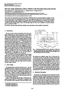
C. Vertical Double-Gate MOSFET The third layout is called vertical double-gate MOSFET as illustrated in Fig 5 [4]. This layout is quite similar to FinFET that has a silicon ridge of nanometer in thickness, which is actually acted as an active area of the transistor. The different between this layout with the FinFET are the current flow is perpendicular to the surface and there is no SOI substrate being implemented. There is only one sub 100nm lithography to define the ridge is required. The channel length of the vertical double-gate MOSFET can be adjusted by ion implantation and diffusion [4]. The main problem of this concept is the parasitic effect that can lower the current. However, this parasitic effect or capacitance can be overcome by compensation implantation technique. The main advantage of vertical double-gate MOSFET is it possesses two gate electrodes with formation of two inversion channel, thus has the ability of doubling the device drive current (ION).
Fig. 5: Vertical Double Gate MOSFET [4]
The vertical DG-MOSFET device could be fabricated by channel engineering method. The device were designed based on ion implantation technique, epitaxial growth and retarded etching to form the silicon pillars [5]. The main objectives of this vertical DG-MOSFET device were to double the drive current (ION) and to well control the subs-threshold swing (SS). By applying vertical DG-MOSFET architecture, the drive current is expected to be more than 0. 2mA while subs-threshold swing (SS) is expected to be in the range of 60mV/dec to 90m V/dec. The drive current (ION) must be kept in high value because it represents the driving capability of
ISSN : 0975-4024
Vol 6 No 5 Oct-Nov 2014
2072
K.E.Kaharudin et al. / International Journal of Engineering and Technology (IJET)
the device. The drive current (ION) must be high enough to trigger the device into on-state condition. Meanwhile, subs-threshold swing (SS) is not recommended to be high because it will delay the switching operation from off-state to on-state condition of the device. A perfect subs-threshold swing (SS) will ensure the device to switch instantly from ‘off’ to ‘on’ or vice versa. According to International Technology Roadmap Semiconductor (ITRS) 2012, the gate length of the multigate device in the year of 2014 is predicted to be at 18 nm [6]. Meanwhile, the threshold voltage (VTH) must be kept at nominal value of 0.207V [6]. To implement such design criteria, thorough investigation had to be done especially in constructing the silicon pillar. The silicon pillar has to form a vertically shaped channel that is capable of carrying a high electric current. Other important output response characteristics that have to be considered is known as leakage current (IOFF) and drain induced barrier lowering (DIBL). Leakage current (IOFF) required to be small as possible because it would affect the performance of the device. The large IOFF contributes to power losses even there is no gate voltage (VG) applied. DIBL occurs when the depletion region of the drain and the source interacts with each other near the channel surface which eventually resulting in lowering the source potential height [7]. Normally, DIBL can be reduced by halo implantation technique. Halo doping has been capable of the shield the channel from the electric field. The layout of 18nm vertical DGMOSFET device simulated by using SILVACO ATHENA module is shown in Fig. 6. IV. CHANNEL ENGINEERING IN DOUBLE-GATE MOSFET There are many problems have occurred in conventional MOSFET, especially short channel effect (SCEs). Examples of SCEs include VTH roll off, drain induced barrier lowering (DIBL), hot electron and etc [7]. Multigate and surround gate MOSFET layout have been proposed to overcome this problem. FinFET and Vertical Double-gate MOSFET are the types that extensively being studied nowadays. In practical, the way to minimize SCEs is to reduce oxide thickness and gate controlled depletion width. This will lead to the increment of channel doping concentration. Channel engineering will then be applied in order to further minimize SCEs in both SOI and bulk devices.
Fig. 6: Layout of Vertical Double Gate MOSFET
The research’s work conducted by Yadav and Rana (2012) proved that channel engineering could control the SCEs [8]. They implemented different level of channel doping concentration in order to observe the effect on the various output responses. From the experiment, they founded that channel doping control could adjust threshold voltage and SCEs as the device’s size shrinking. However, channel doping could not be increased beyond the certain limit because some output responses like sub-threshold swing and DIBL were opposite in nature. If one output response was improved, the other one became worst.
ISSN : 0975-4024
Vol 6 No 5 Oct-Nov 2014
2073
K.E.Kaharudin et al. / International Journal of Engineering and Technology (IJET)
From the research made by Kumari et al. (2012), channel engineering was conducted by using two methods, which were low-high vertical non-uniform channel doping and halo doping [7]. The objective of their research was to increase the drive current (ION) without increasing of state leakage current (IOFF). Their researches were based on developing SOI FinFET by using Silvaco Devedit. Their research’s focus areas were on device parameters such as VTH, tranconductance and mobility degradation. The effect of halo doping on the extracted device parameter was studied. From the observation made, it was concluded that halo doping shielded the channel from electric field and hence VTH was increased as halo doping level was increased [7]. Based on research conducted by Ismail Saad et al., (2011), vertical Double-Gate MOSFET had advantages of controlled gate length by relax photolithography process, high drive current per unit silicon and developed channel length from packaging density [9]. The vertical MOSFET structure usually utilized undoped body due to the ability to avoid the dopant fluctuation effect which will contribute to the variation of the VTH and ION. However, due to technological constraint with the tunable work function, channel doping remains the alternative way to control VTH [9]. V. PROCESS PARAMETERS VARIATION Process variations have become a critical issue in today’s high-performance circuit design as technology keeps scaling down. As technology continues to scale down, process variation has more significant impact on circuit performance. Small dimension devices operating at low supply voltages show an in increased sensitivity to parameter variations. It is therefore, essential to characterize and control the parameter fluctuations to improve the performance and yield of integrated circuits. Increased process parameter variation has been recognized as one of the major roadblocks to further technology scaling. The corner-based design approach treats all variations as random. As the corner spread is increasing with technology scaling, simultaneously satisfying performance, power and yield requirements becomes challenging [10]. In order to better account for the variability in the design process, it is necessary to distinguish systematic shifts in parameter values from truly random one. The increase in MOSFET variability affects many aspects of technology development, manufacturing, and design [11]. With MOSFET scale becomes smaller, the number of atoms in the semiconductor material becoming fewer thereby amplifying the dependence of the transistor characteristics with process parameters variation [12]. The source of process variations is organized into two types, which are global variations and local variations. Global variations usually involve in material properties such as wafer, implant dose, oxide thickness and many more. This type of variation actually affects the performance in the digital system such as switching speed, dynamic power and gain in analog system [12]. These types of variation can be modeled since they are systematic and predicted. Local variations normally arise from random microscopic process variation. These variations are randomly distributed are unpredictable. For 130nm technology, local variations are about 30% from the overall variation [13]. One of the examples for local variation is process parameter fluctuations that may result in the variation of threshold voltage and sheet resistance. The variation of threshold voltage can also be due to the variation of surface charge and oxide thickness. VI. METHODS TO STUDY PROCESS PARAMETERS VARIATION A. Simulation Study Silvaco ATHENA and ATLAS module is an example of a TCAD tool that can be manipulated effectively in studying the downscaling process. It would give the economic and speed edge to the traditional way of doing things. Semiconductor TCAD tools are computer programs, which allow for the creation, fabrication and simulation of semiconductor devices. These simulations provided the opportunity to study the effect of different device parameters on the overall device performance [14]. Optimization of these devices using the TCAD tools requires many hours of lab simulation time. Several aspects of each device were selected for optimization. Once the device characteristics were selected for optimization, the process of device simulation began. First, each parameter was tested individually for its effect on device performance as a whole. Once several plots were obtained that indicated the particular parameter’s effect on device performance, improved values could then be selected for the device. Several simulations needed to be run to find improved values for each device parameter, until an optimal value was reached. Once an optimal value was reached for each of the device parameters, the improved parameters were then recombined into a single device. Once these new values were all present in a single device, they were again simulated and adjusted to optimize based upon their combined effects, to ultimately produce an optimal device configuration [15]. B. Statistical Modeling Statistical modeling is one of the important tools to identify the input process parameters that contribute most impact on the MOSFET device characteristics. All the device modeling need to do optimizations approach to get optimum performance for CMOS technology [10]. The optimization of manufacturing operations and products is one of the vital industrial functions to improve the product performance as well as to save manufacturing cost. ISSN : 0975-4024
Vol 6 No 5 Oct-Nov 2014
2074
K.E.Kaharudin et al. / International Journal of Engineering and Technology (IJET)
Many researchers have proposed method to adjust the threshold voltage (VTH), sheet resistance (Rs) and other response characteristics. Statistical methods are often carried out to optimize the process parameter variation. For example, Monte Carlo analysis is widely used to analyze parameter variability to generate response distributions. Although this method would produce very accurate analysis, it is still not very efficient when dealing with a large number of variables. Another approach of analyzing the effect of process variation is known as Response Surface Methodology (RSM). The advantage of using RSM is it can predict the response accurately if the model is well established. However, RSM requires a lot of data points in order to fit the second-order polynomial which is not cost effective, especially in the semiconductor industry [16]. One of the most systematic and efficient ways to achieve robust design is to use an optimization method of designing experiments based on Taguchi Methods. Taguchi Methods provide the most efficient and viable solution in such cases with minimal experimental trials. Taguchi suggests that to analyzing signal-to-noise ratios (S/N) by using the conceptual approach that involves graphing the effects and visually identifying the factors that show to be significant. The slopes of the lines also show the relative influence of the factor to the variability of results. The Pareto ANOVA method is used to analyze the data for process optimization. This is a quick and easy method for analyzing results of parameter design that does not require an ANOVA table and does not use F-tests. This method enables the significance of factors to be evaluated by Pareto type analysis. It also allows the optimal levels of factors to be obtained [17]. 2 k-factorial design is also one of the optimization techniques based on designing the experiments. In next section, more detail information about both Taguchi and 2kfactorial design methods will be further discussed. VII. TAGUCHI METHOD Taguchi method has been introduced by Dr. Genichi Taguchi, and it is proven to be valuable tools in various fields of engineering [18]. Taguchi method is based on an approach which is completely different from the conventional practices of quality engineering. The methodology emphasizes on designing the quality into the products and processes, whereas the usual practice relies upon inspection. Taguchi essentially utilized the conventional statistical tools, but it is simplified by identifying as set of guidelines for experiment layout and the analysis of the result. Taguchi experimental design approach is suitable for a wide range of applications that involves many factors. A. Orthogonal Array One of the major advantages of Taguchi Method in optimization purpose is the presence of Orthogonal Arrays (OA) for the design. Orthogonal Arrays (OA) greatly simplifies the task of designing experiment, especially when it is involved with many experiment runs. The Taguchi methods help in reducing the number of experiments required in optimization purpose [19]. B. Experiment Design Strategy Taguchi method is constructed by a special set of orthogonal arrays (OAs) to layout some experiments. Table I shows a common OA for three-level factors. This array is designed by the symbol of L9, and it is used to design experiment involving up to four, 3 level factors. The array has nine rows and four columns. Each row represents a trial experiment with factor levels indicated by the numbers in the row. The vertical columns correspond to the factors specified in the study [20]. Each column contains three level 1, three level 2, and three level 3 conditions for the factor assigned to the column. That means each column has the equal number of levels. Thus, all four columns of certain level are orthogonal to each other. The noise factor is actually to acquire four different reading for each row, which will improve the robustness of the experiment. TABLE I L9 Experiment with Two Levels of Noise Factor [19]
Exp No. 1 2 3 4 5 6 7 8 9
ISSN : 0975-4024
A 1 1 1 2 2 2 3 3 3
Control Factors B C 1 1 2 2 3 3 1 2 2 3 3 1 1 3 2 1 3 2
D 1 2 3 3 1 2 2 3 1
Vol 6 No 5 Oct-Nov 2014
Measurements to Capture Noise E1F1 E1F2 E2F1 E2F2 Y11 Y12 Y13 Y14 Y21 Y21 Y23 Y24 Y31 Y32 Y33 Y34 Y41 Y42 Y43 Y44 Y51 Y52 Y53 Y54 Y61 Y62 Y63 Y64 Y71 Y72 Y73 Y74 Y81 Y82 Y83 Y84 Y91 Y92 Y93 Y94
2075
K.E.Kaharudin et al. / International Journal of Engineering and Technology (IJET)
The OA facilitates the experiment design process. In designing an experiment, it is important select the most suitable orthogonal array, assign the factors to the appropriate columns, and finally, describe the combinations of individual experiments called trial experiments. The array forces all experimenters to design almost identical experiments. Experimenters may select different designations for the columns, but the nine trial runs will include all combinations independent of column definition. Thus, OA assures consistency of design by different experimenters. C. Signal-to-Noise (S/N) Ratio There are three categories of the performance characteristics in the analysis of the S/N ratio which are known as lower-the-better, higher-the-better and nominal-the-better [21]. The S/N ratio for each level of process parameters is computed based on the S/N analysis. Regardless of the type of the performance characteristic, the larger S/N ratio is always to be recognized as the better performance characteristic [22, 23]. Therefore, the optimal level of the process parameters is the one with the greatest S/N ratio. The S/N ratio (Nominal-the-best), η can be expressed as [24]:
μ2 2 σ
η = 10 Log 10
(1)
whereas:
μ=
Yi + ....... + Yn n
(2)
and n
σ2 =
(Yi − μ )2 i =1
(3)
n−1
While n is the number of tests and Yi is the experimental value of the threshold voltage, µ is mean and σ2 is variance. In the nominal-the best, there are two types of factor to determine, which are dominant and adjustment factors. The S/N ratio, η of the smaller-the-best quality characteristics can be expressed as [24]:
(
)
1 Y12 + Y22 + .... + Yn2 n
η = 10 Log 10
(4)
While n is the number of tests and Yn is the experimental value of the response characteristics. In order to further investigate the effect of the process parameters towards responses, a statistical analysis of variance (ANOVA) is performed. Statistical analysis of variance (ANOVA) has the capability to determine which process parameters contribute the most significant impact on output responses. With the S/N and ANOVA analysis, the optimal combinations of the process parameters are able to be predicted. D. Analysis of Result In the Taguchi method, the results of the experiments are analyzed to achieve one or more of the following three objectives which are to establish the best or the optimum condition for a product or a process, to investigate the contribution of individual factors and to investigate the response under the optimum condition. The optimum condition is identified by studying the main effects of each of the factors. The process involves minor arithmetic manipulation of the numerical results. The main effects indicate the basic pattern of the influence of the factors. By knowing the characteristics, i.e., whether a higher or lower value produces the preferred result, the levels of the factors which are expected to produce the best result can be predicted. The knowledge of the contribution of individual factors is a key to decide the nature of the control to be established through a process. The analysis of variance (ANOVA) is the statistical analysis commonly applied to the results of the experiment in order to determine the percent contribution of each factor. The study of ANOVA table for a given analysis will assist experimenters to determine which of the factors need to be controlled and, which is not. Once the optimum condition is determined, it is usually a good practice to run a confirmation experiment. It is possible to estimate performance at the optimum condition from the result of the experiments conducted at a non-optimum condition. It should be noted that the optimum condition may not necessarily be among the many experiments already carried out, as the OA represents on a small fraction of the possibilities. Taguchi method implies two different routes to carry out the complete analysis. First, the standard approach, where the result of single run, or the average of repetitive runs, are processed through main effect and ANOVA analyses as identified above. The second approach, which is recommended for multiple runs, is by using signal to noise ratio (S/N) for the same steps in the analysis. S/N analysis determines the most robust set of experiments from process variations within the results [25].
ISSN : 0975-4024
Vol 6 No 5 Oct-Nov 2014
2076
K.E.Kaharudin et al. / International Journal of Engineering and Technology (IJET)
VIII. 2K-FACTORIAL DESIGN 2k-factorial design is a popular method based on statistical consideration, which contributes the most significant information about factor effects towards certain problems, including interaction effects between variables. This method is able to evaluate all process variables simultaneously in determining which variables would give the most significant impact toward responses. All variables are known as factors and each of them represents the different level of value for investigating the purpose [26], [27]. The analysis procedures for 2kfactorial design are to estimate factors effect, to build an initial model, to investigate the significant factors effect, to analyze residual error, to remodel if required and to translate the results. A. Advantages of 2k-factorial Design 2k-factorial design is very useful in developing and modifying the process. This type of factorial design possesses ‘k’ factor, and each of them consists of two levels. This design offers very easy and efficient analysis [28]. For analysis that involves many factors, single replicate design could be implemented. It also could be used for filtering test if there are many factors to be considered. This is because of not every factor will produce small residual errors. The final results are probably not very accurate if only once the experiment for each combination of factors is implemented. B. Experiment Design Strategy 2k-factorial design is developed by a special set of orthogonal arrays (OAs) to layout some experiments. Table II [24] shows the example of testing matrices of 2k-factorial for orthogonal arrays of 24. For this design’s example, four factors will be investigated, which named as factor A, B, C and D. Therefore, the required 2kfactorial design is 24. Sign ‘–‘ and ‘+’ of each lines indicates the set for variable A and B in each run. TABLE III Testing Matrices For 2k-Factorial 24
Exp no. 1 2 3 4 5 6 7 8 9 10 11 12 13 14 15 16
Run Label (1) a b ab c ac bc abc d ad bd abd cd acd bcd abcd
Factor A -1 1 -1 1 -1 1 -1 1 -1 1 -1 1 -1 1 -1 1
Factor B -1 -1 1 1 -1 -1 1 1 -1 -1 1 1 -1 -1 1 1
Factor C -1 -1 -1 -1 1 1 1 1 -1 -1 -1 -1 1 1 1 1
Factor D -1 -1 -1 -1 -1 -1 -1 -1 1 1 1 1 1 1 1 1
C. Data Analysis of 2k-factorial Data analysis is initially implemented by developing normal probability plot for effects estimation. Sign ‘–‘ and ‘+’ are used for contrast 2k-factorial of 24. Contrast mathematical formula as shown as in Eqn. (5). Based on contrast analysis, effect estimation and sums of squares could be calculated by using the formula in Eqn. (6) and Eqn. (7) [28]. Contrast formula: Contrast AB .......K = (a ± 1)(b ± 1).......(k ± 1)
(5)
Estimation Effect formula: AB .......K =
2 n2 k
(Contrast AB.......K )
(6)
(Contrast AB .......K )2
(7)
Sums of squares formula: SS AB .......K =
1 n2
k
With n represents total repetitions and k for total factors. From estimation effects formula, normal probability plot can be built. Example of the normal probability plot is shown as in Fig 7. Factors located in the straight line ISSN : 0975-4024
Vol 6 No 5 Oct-Nov 2014
2077
K.E.Kaharudin et al. / International Journal of Engineering and Technology (IJET)
are the factors that will be ignored. Meanwhile, factors that are spread away from the straight line will be considered as significant factors.
Fig. 7 Example Plot of Normal Probabilities
There might be some difficulties exist in 2k-factorial design method, which is to estimate the linearity of factor effects. First-order main effects model is shown as in Eqn. (8) where interaction terms are included noted as βijxixj: k
y = β 0 + β j χ j + β ij χ i χ j + ∈ j −1
(8)
i< j
However, there will be some situation where the curves in response function are not perfectly modelled by Eqn. (8). In this case, logical model will be considered, which is known as second order response surface model by using Eqn. (9): k
k
y = β 0 + β j χ j + β ij χ i χ j + β jj χ j 2 + ∈ j −1
i< j
(9)
j −i
In Equation (9), βjj represents second order or quadratic effect [26]. Middle point is added in experiment set for obtaining additional information such as residual error and investigating the curve from second order effect [29]. IX. CONCLUSION In conclusion, the impact of channel doping on DG-MOSFET parameters was investigated by other researchers. They were only executed by utilizing numerical and simulation analysis. Their researches were actually conducted to investigate how the channel or body doping would impact on the device’s characteristic. It was observed that by changing the channel doping, the output responses of the device can be adjusted as desired. However, it was only able to satisfy one or two response’s characteristics not all. It was because each individual response characteristic was opposite in nature. In other words, if one of the parameters is gotten improved while the other parameters will get worse. Therefore, in order to optimize all the response’s characteristics, more input process parameters have to be considered. For that purpose, the effects of input process parameters upon their corresponding responses have to be investigated. The way to implement that is by implementing statistical modeling such as Taguchi and 2k-factorial design methods. By recognizing which input process parameters contribute the most significant impact on responses, the optimal fabrication recipe can be predicted. Therefore, regardless the type of the MOSFET device, input process parameters variation is still an important factor to be considered in MOSFET fabrication. Statistical modeling is recommended to be implemented in multi-gate MOSFET architecture in order to minimize the variation of process parameters. Furthermore, interaction between input process parameters of the device can be studied. Hence, the optimum solution to obtain robust design of the device is able to be predicted. ACKNOWLEDGMENT The authors would like to thanks to the Ministry of Higher Education (MOHE) for sponsoring this work under project (PJP/2012/FKEKK(11C)/S01111) and Faculty of Electronics and Computer Engineering (FKEKK), Universiti Teknikal Malaysia Melaka (UTeM) for the moral support throughout the project.
ISSN : 0975-4024
Vol 6 No 5 Oct-Nov 2014
2078
K.E.Kaharudin et al. / International Journal of Engineering and Technology (IJET)
REFERENCES [1] [2] [3] [4] [5] [6] [7] [8] [9] [10] [11] [12] [13] [14] [15] [16] [17] [18] [19] [20] [21] [22] [23] [24] [25] [26] [27] [28] [29]
Isabelle Ferain, Cynthia A. Colinge and Jean-Pierre Colinge., “Multigate Transistor as the Future of Classical Metal-oxidesemiconductor Field-effect Transistors”, Nature, vol 479, pp. 310-316, 2011. Wai-Kai Chen , “The VLSI Handbook”. CRC Press. Fig. 2.28, p. 2–22. ISBN 0-8493-4199-X 2006. Mathew et al., “Vertical CMOS Double Gate MOSFET with notched poly gates”, Motorola Inc-Semiconductor Products SectorAPDER, 3501 Ed Bluestein blvd. Austin TX-7872, U.S.A., 2005. J. Moers et al., “Vertical p-Channel Double-Gate Mosfets”, Institute of Thin Films and Interfaces (ISG), Research Center Jülich; 52425 Jülich, Germany, 2007. Ismail Saad and Razali Ismail, “Design and Simulation of 50nm Vertical Double-Gate MOSFET (VDGM)”, ICSE2006. Proc, pp. 549553, 2006. ITRS 2012 Report; http://www.itrs.net Riti Kumari, Manish Goswami and B. R. Singh., “The Impact of Channel Engineering on Short Channel Behaviour of Nano FinFETs”, International Journal of Nanoscience, vol. 11, No. 2, 2012. V. K. Yadav and A. K. Rana., “Impact of Channel Doping on DG-MOSFET Parameters in Nano Regime-Tcad Simulation”, International Journal of computer Application, Vol. 37 to 11, pp. 36-41, 2012. Ismail Saad et al., “Performance Design and Simulation Analysis of Vertical Double Gate MOSFET (VDGM)”, UKSim 13th International Conference on Modelling and Simulation, pp. 518-521, 2011. S. Shedabale, H. Ramakrishnan, G. Russell, A. Yakovlev, and S. Chattopadhyay., "Statistical Modelling of the Variation in Advanced Process Technologies using a Multi-level Partitioned Response Surface Approach", IET Circuits, Devices and Systems Journal, 2008. R. S. Santiesteban, G. C. Abeln, T. E. Beatty, and R. Osvaldo, “Effect of tilt angle variations in halo implant on VTH values for 0.14µm cmos devices”, IEEE Transactions on Semiconductor Manufacturing, vol. 16(4), pp. 653-655, 2003. W. J. Cho, J. H. Yang, K. Im, J. Oh, and S. Lee., “Fabrication and process simulation of soi mosfets with a 30-nm gate length”, Journal of the Korean Physical Society, vol. 43(5), pp. 892-897, 2003. H. Xiao, “Introduction to Semiconductor Manufacturing Technologies”, Prentice Hall, Upper Sadle River, New Jersey, 2001. F. Salehuddin, I.Ahmad, F.A.Hamid, A.Zaharim, “Optimization of Process Parameters Variability in 45nm PMOS Device Using Taguchi Method”. International Journal of Applied Sciences, Vol. 11, No. 7, pp. 1261-1266, 2011. S. Williams and K. Varahramyan., “A New TCAD-Based Statistical Methodology for the Optimization and Sensitivity Analysis of Semiconductor Technologies”, IEEE Transaction on Semiconductor Manufacturing, Vol. 13, No. 2, May 2000. P. Chiang and M. R. Chen., 2001, “Device optimization using response surface methodology with orthogonal arrays”, IEEE Int. Workshop on statistical Methodology, pp. 17-20, 2000. F. Salehuddin, I. Ahmad, F. A. Hamid, and A. Zaharim, u. Hashim and P.R. Apte., “Optimization of input process parameters variation on threshold voltage in 45nm NMOS device”, International Journal of the Physical Sciences Vol. 6, No.30, pp. 7026 – 7034, 2011. Ranjit K Roy, “A Primer on the Taguchi Method”, Library of Congress Catalogin-in-Publicating-Data., 1990. Phadke MS., “Quality Engineering Using Robust Design”, Pearson Education, 2008. Ranjit K. Roy., “DOE-I Basic Design of Experiments (The Taguchi Approach)”, Nutec Inc. Quality Engineering Seminar and Software, 2004. Syros GP., “Die casting process optimization using Taguchi methods”. J. Mater. Proc. Technol”, 135(1): 68-74, 2003. F.Salehuddin, I.Ahmad, F.A.Hamid, A.Zaharim, “Influence of HALO and Source/Drain Implantation on Threshold Voltage in 45nm PMOS Device”. Australian Journal of Basic and Applied Sciences, Vol. 5, No. 1, pp. 55-61, 2011. Naidu NVR., “Mathematical model for quality cost optimization, Robotics and Computer-integrated Manufacturing”. Int. Conf. Flexible Automat. Intell. Manuf., 24(6): 811-815, 2008. Phadke MS., “Quality Engineering Using Robust Design”. Pearson Education, Inc. and Dorling Kindersley Publishing, Inc., 1998. Nalbant M, Gokkaya H, Sur G., “Application of Taguchi method in the optimization of cutting parameters for surface roughness turning," Int, J. Design, 28: 1379-1385, 2007 Montgomery, D.C, “Design and Analysis of Experiment”, Fifth Edition New York: John Wiley & Son Inc., 2001. Costa, C.B.B., Rivera, E.A.C., Rezende, M.C.A.F., Maciel, M.R.W. & Filho, R.M, “Prior detection of Genetic Algorithm Significant Parameters: Coupling Factorial Design Technique to Genetic Algorithm”, Chemical Engineering Science Vol 62, pp. 4780-4801, 2007. Montgomery, D.C, “Introduction to Statistical Quality Control”, Fifth Edition New York: John Wiley & Son Inc., 2005. Yu, Z. Peldszus, S. & Huck, P. M., “Optimization of Gas Chromatographic-Mass Spectrometric Analysis of Selected Pharmaceuticals and Endocrine-Disrupting Substances in Water using Factorial Experiment Design”, Journal of Chromatography A. 1148, pp. 65-77, 2007.
ISSN : 0975-4024
Vol 6 No 5 Oct-Nov 2014
2079