APPLIED PHYSICS LETTERS 96, 103116 共2010兲
Design constraints and guidelines for CdS/CdTe nanopillar based photovoltaics Rehan Kapadia, Zhiyong Fan, and Ali Javeya兲 Department of Electrical Engineering and Computer Sciences, University of California at Berkeley, Berkeley, California 94720, USA; Berkeley Sensor and Actuator Center, University of California at Berkeley, Berkeley, California 94720, USA; and Materials Sciences Division, Lawrence Berkeley National Laboratory, Berkeley, California 94720, USA
共Received 13 January 2010; accepted 9 February 2010; published online 11 March 2010兲 The performance dependence of a CdS/CdTe nanopillar solar cell on various device and materials parameters is explored while examining its performance limits through detailed device modeling. The optimized cell enables efficiencies ⬎ ⬃ 20% with minimal short circuit current dependence on bulk minority carrier diffusion length, demonstrating the efficient collection of photogenerated carriers, therefore, lowering the materials quality and purity constraints. Given the large p-n junction interface area, the interface recombination velocity is shown to have detrimental effect on the device performance of nanopillar solar cells. In that regard, the CdS/CdTe material system is optimal due to its low interface recombination velocity. © 2010 American Institute of Physics. 关doi:10.1063/1.3340938兴
a兲
Electronic mail:
[email protected].
0003-6951/2010/96共10兲/103116/3/$30.00
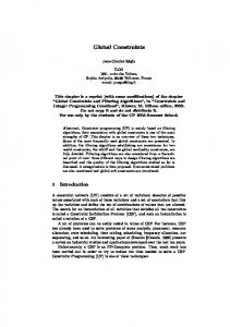
The SNOP cell is simulated by defining half of a twodimensional cross section of the device 关Fig. 1共b兲兴 and then assuming cylindrical symmetry in the device equations, using a scheme previously used for Si core/shell NW cells.2 However, the simulated SNOP cell consisted of a square lattice of NPLs embedded in a CdTe film. This gives rise to a square “unit cell” as shown in Fig. 1共c兲, which is not accurately represented by the cylindrical structure in Fig. 1共b兲. Thus, to simulate the results for a SNOP-cell with a given pitch, multiple simulations with fixed NPL radius and increasing outer radius were simulated as shown in Fig. 1共c兲. The parameters of the SNOP cell were then calculated using 2 the formula: p = p共r1兲 − ⌺A共ri , ri+1兲关共p共ri兲兲 − p共ri+1兲兴 / 关ri+1 2 − ri 兴; where p represents the parameter of interest 共i.e., conversion efficiency, , open circuit voltage, Voc, or photocurrent, Jsc兲, p共r1兲 is the parameter evaluated at radius r1, A共ri,ri+1兲 is the area bounded by circles of radius ri, ri+1, and the square. This approximation corrects for the missing area through the 1st order Taylor expansion terms from each of the larger diameter simulations. It should be noted that this result is only valid when the junctions are sufficiently far apart such that their depletion regions do not interact. -./ !) *+,
#?
!"# %&'( -0/
@' ABCCB( BDC.4C
1.!&23
% &$