Development Aspects of an Integrated Pyroelectric Array Incorporating a Thin PZT Film and Radiation Collectors CHRISTOPHER SHAW, SPARTACO LANDI, ROGER WHATMORE, PAUL KIRBY
[email protected] Abstract Work is being undertaken to produce an uncooled pyroelectric infra-red detector array which incorporates within its structure, an array of radiation collectors made by the bulk micromachining of silicon. Development aspects of the processing route are presented here.
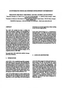
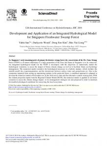
Keywords: Pyroelectric Array, Micromachining, corona poling. AIP:77.70.+a 77.84.Dy 52.80.Hc 87.80.Mj Introduction Typical commercial versions of arrays of pyroelectric detectors are manufactured from bulk ceramic materials which are lapped and polished, laser machined to thermally isolate the elements and flip-chip bonded to silicon chip circuitry. Work at Cranfield is being undertaken to develop a pyroelectric array, which incorporates within its structure an array of radiation collectors via a silicon wafer processing route. Silicon Wafer Processing Figure 1 shows the schematic drawing of the early prototype array structure where simple radiation collectors have been formed by the anisotropic etching of silicon as pyramidal wells by tetramethyl ammonium hydroxide (TMAH). Corona poling potentially offers a practical route to poling large areas of thin film PZT samples particularly where the presence of pinhole defects prevents the use of conventional contact poling methods. Figure 2 summarises the two multiple pin poling set-ups investigated for the poling of 100mm PZT coated substrates.
Corona Poling Qualitative experimental observations showed that no poling occurred without an audible corona “hiss”. For an initial fixed height of h=~15mm, the corona discharge field was smaller for the higher pin density case. However, on viewing the visible discharge in the dark for this set-up, it was evident that only the outermost pins were discharging. For the low pin density case all the pins showed a discharge at this height. When the height was reduced to ~9mm, all the pins in both the low and high density cases were seen to discharge. The observation of visible cloudy areas on the sample coincident with the corona pin positions was the first evidence of poling. This was shown to be microcracking within the PZT probably as a result of stress. However, in large areas, it was still possible to measure array elements which showed the characteristic decrease in dielectric constant associated with poling, compared to the unpoled state.
Silicon Anisotropic Wet Etching Criteria
To achieve an acceptable etch rate (25μm/hr.) of silicon and because the use of Apiezon™ wax to protect the back face processing limited the etch temperature to ~70°C, a 12.5wt% aqueous TMAH solution was required. Initial etch runs suggested that degradation effects from the wax reaction with the TMAH was effecting the uniformity of the etch. Subsequent encapsulation of the edge of the sample with silicone rubber prevented degradation of the wax. The flow of the etchant over the array was an important criteria also to maintain uniformity of etch, across the high density of 16x16 elements per array. The best uniformity was achieved by orienting the sample at 45°face down towards the stirring rod. Ideally, for the pyramidal wells to act as radiation collectors they should have smooth walls. The initial 12.5wt% TMAH solution achieved an acceptable etch rate, but the walls showed
a crater-like topology, as well as a significant undercut of the SiO2 mask. Work by Tabata et. al. (1) had reported that using TMAH solutions above 22wt% produced a smooth wall etch, although at 70°C the etch rate was relatively slow. As a result, a two step etch process was applied to the array structures involving an initial slow ~10μm etch in a 25wt% TMAH solution followed by the 12.5wt% etch to completion. Figure 3 shows the improvement in wall smoothness achieved by the two step etch. The undercut of the SiO2 was also controlled producing uniform apertures and membranes, and a reduction of wall failures between neighbouring elements. Conclusions The multipin corona poling set-up has proved successful at poling intact localised areas of PZT, but has introduced development issues. Apart from the set-up requiring identical pins set at an identical height, there seems to be a relationship between pin separation(density) and height above sample, which effects the uniformity of discharge across the sample. This needs to be addressed to reduce undesirable microcracking across the sample. Development of a two step TMAH silicon etch process has proved successful in producing a uniform etch across an array of 16x16 elements. Identical pyramidal radiation collectors are required to allow comparative future testing.
References 1. Tabata O, Asahi R, Funabashi H, Shimaoka K, Sugiyama S: Sensors and Actuators. 1992; A34; 51-57. Figure 1. Schematic prototype array structure. Figure 2. Multipin Corona Poling Set-ups. Figure 3. Comparison of etch uniformity for one-and two-step TMAH etch processes.
Active Pyroelectric Element Area
Electrical Contact Point
Cr/Au Top Electrode
Back Face View
PZT Patterned Ti/Pt Bottom Electrode
TiO2 Si
Si
Si
Si SiO2
Patterned SiO2 Mask
Position of Active Pyroelectric Element Area
Cross-section
Front Face View
Figure 1
Radiation Collector (54.7º Anisotropic Wet Etched Well)
+ V1
+
d1
h
V2
d2
h
Sample
Earth Plate High Pin Density
Figure 2
Lower Pin Density
25wt%+12.5wt% TMAH etch
12.5wt% TMAH etch Walls
500µm
Front Array Apertures
500µm
Figure 3