Freescale Semiconductor. Tempe, Arizona 85284. [r54143, lee.hartin]@freescale.com. AbstractâDecoupling capacitors are widely used to reduce power supply ...
Efficient Placement of Distributed On-Chip Decoupling Capacitors in Nanoscale ICs Mikhail Popovich, Eby G. Friedman
Radu M. Secareanu, Olin L. Hartin
Department of Electrical and Computer Engineering University of Rochester Rochester, New York 14627 [nhlover, friedman]@ece.rochester.edu
MMSTL Freescale Semiconductor Tempe, Arizona 85284 [r54143, lee.hartin]@freescale.com
Abstract— Decoupling capacitors are widely used to reduce power supply noise. On-chip decoupling capacitors have traditionally been allocated into the white space available on the die based on an unsystematic or ad hoc approach. In this way, large decoupling capacitors are often placed at a significant distance from the current load, compromising the signal integrity of the system. This issue of power delivery cannot be alleviated by simply increasing the size of the on-chip decoupling capacitors. To be effective, the on-chip decoupling capacitors should be placed physically close to the current loads. The area occupied by the onchip decoupling capacitor, however, is directly proportional to the magnitude of the capacitor. The minimum impedance between the on-chip decoupling capacitor and the current load is therefore fundamentally affected by the magnitude of the capacitor. A distributed on-chip decoupling capacitor network is proposed in this paper. A system of distributed on-chip decoupling capacitors is shown to provide an efficient solution for providing the required on-chip decoupling capacitance under existing technology constraints. In a system of distributed onchip decoupling capacitors, each capacitor is sized based on the parasitic impedance of the power distribution grid. Various tradeoffs in a system of distributed on-chip decoupling capacitors are also discussed. Related simulation results for typical values of on-chip parasitic resistance are also presented. An analytic solution is shown to provide accurate distributed system. The worst case error is 0.003% as compared to SPICE. Techniques presented in this paper are applicable not only for current technologies, but also provide an efficient placement of the onchip decoupling capacitors in future technology generations. Index Terms— Power distribution systems, power distribution grids, decoupling capacitors, power noise
I. I NTRODUCTION Decoupling capacitors are widely used to manage power supply noise [1]. Decoupling capacitors are an effective way to reduce the impedance of power delivery systems operating at high frequencies [2], [3]. A decoupling capacitor acts as a local reservoir of charge, which is released when the power supply voltage at a particular current load drops below some
This research is supported in part by the Semiconductor Research Corporation under Contract No. 2004-TJ-1207, the National Science Foundation under Contract Nos. CCR-0304574 and CCF-0541206, grants from the New York State Office of Science, Technology & Academic Research to the Center for Advanced Technology in Electronic Imaging Systems, and by grants from Intel Corporation, Eastman Kodak Company, Intrinsix Corporation, and Freescale Semiconductor Corporation.
1-4244-1382-6/07/$25.00 ©2007 IEEE
tolerable level. Since the inductance scales slowly [4], the location of the decoupling capacitors significantly affects the design of power/ground (P/G) networks in high performance integrated circuits (ICs) such as microprocessors. At higher frequencies, a distributed system of decoupling capacitors will need to be placed on-chip to effectively manage the power supply noise [5]. The efficacy of decoupling capacitors depends upon the impedance of the conductors connecting the capacitors to the current loads and power sources. As described in [6], a maximum parasitic impedance between the decoupling capacitor and the current load (or power source) exists at which the decoupling capacitor is effective. Alternatively, to be effective, an on-chip decoupling capacitor should be placed such that both the power supply and the current load are located inside the appropriate effective radius [6]. The efficient placement of on-chip decoupling capacitors in nanoscale ICs is the subject of this paper. Unlike the methodology for placing a single lumped on-chip decoupling capacitor presented in [6], a system of distributed on-chip decoupling capacitors is proposed. A design methodology to estimate the parameters of the distributed system of on-chip decoupling capacitors is also presented, permitting allocation of the required on-chip decoupling capacitance under existing technology constraints. The paper is organized as follows. The problem of placing on-chip decoupling capacitors in nanoscale ICs under technology constraints is formulated in Section II. The design of an on-chip distributed decoupling capacitor network is presented in Section III. Various design tradeoffs are discussed in Section IV. Related simulation results for typical values of the on-chip parasitic resistance are discussed in Section V. Some specific conclusions are summarized in Section VI. II. P LACING O N -C HIP D ECOUPLING C APACITORS IN NANOSCALE IC S Decoupling capacitors have traditionally been allocated into the white space (those areas not occupied by the circuit elements) available on the die based on an unsystematic or ad hoc approach [7], [8], as shown in Fig. 1. In this way, decoupling capacitors are often placed at a significant distance from the current load. Conventional approaches for placing onchip decoupling capacitors result in oversized capacitors. The
811
conventional allocation strategy, therefore, results in increased power noise, compromising the signal integrity of an entire system, as illustrated in Fig. 2. This issue of power delivery cannot be alleviated by simply increasing the size of the onchip decoupling capacitors. Furthermore, increasing the size of more distant on-chip decoupling capacitors results in wasted area, increased power, reduced reliability, and higher costs. A new design methodology is therefore required to account for technology trends in nanoscale ICs, such as increasing frequencies, larger die sizes, higher current demands, and reduced noise margins.
minimum impedance between an on-chip capacitor and the current load is fundamentally affected by the magnitude (and therefore the area) of the capacitor. Systematically partitioning the decoupling capacitor solves this issue. A system of on-chip distributed decoupling capacitors is illustrated in Fig. 3.
Vdd
Iload 3 Cdec
2 Cdec
1 Cdec
Fig. 3. A network of distributed on-chip decoupling capacitors. The magnitude of the decoupling capacitors is based on the impedance of the interconnect segment connecting a specific capacitor to a current load. Each decoupling capacitor is designed to only provide charge during a specific time interval.
Fig. 1. Placement of on-chip decoupling capacitors using a conventional approach. Decoupling capacitors are allocated into the white space (those areas not occupied by the circuits elements) available on the die using an unsystematic or ad hoc approach. As a result, the power supply voltage drops below the minimum tolerable level for remote blocks (shown in dark grey). Low noise regions are light grey.
To be effective, a decoupling capacitor should be placed physically close to the current load. This requirement is naturally satisfied in board and package applications, since large capacitors are much smaller than the dimensions of the circuit board (or package) [9]. In this case, a lumped model of the decoupling capacitor provides sufficient accuracy [10].
Vdd
Cdec
Iload
Fig. 2. A conventional on-chip decoupling capacitor. Typically, a large decoupling capacitor is placed at a greater distance from the current load due to physical limitations. Current flowing through the long power/ground lines results in large voltage fluctuations across the terminals of the current load.
The size of an on-chip decoupling capacitor, however, is directly proportional to the area occupied by the capacitor and can require a significant portion of the on-chip area. The
In a system of distributed on-chip decoupling capacitors, each decoupling capacitor is sized based on the impedance of the interconnect segment connecting a capacitor to a current load. A particular capacitor only provides charge to a current load during a short period. The rationale behind the proposed scheme can be explained as follows. The capacitor closest to the current load is engaged immediately after the switching cycle is initiated. Once the first capacitor is depleted, the next capacitor is activated, providing a large portion of the total current drawn by the load. This procedure is repeated until the last capacitor becomes active. Similar to the hierarchical placement of decoupling capacitors presented in [3], [11], the proposed technique provides an efficient solution for providing the required on-chip decoupling capacitance based on specified capacitance density constraints. A system of distributed onchip decoupling capacitors should therefore be utilized to provide a low impedance, cost effective power delivery network in nanoscale ICs. III. D ESIGN OF AN O N -C HIP D ISTRIBUTED D ECOUPLING C APACITOR N ETWORK As described in Section II, a system of distributed on-chip decoupling capacitors is an efficient solution for providing the required on-chip decoupling capacitance based on the maximum capacitance density available in a particular technology. A physical model of the proposed technique is illustrated in Fig. 4. For simplicity, two decoupling capacitors are assumed to provide the required charge drawn by the current load. Note that as the capacitor is placed farther from the current load, the magnitude of an on-chip decoupling capacitor increases due to relaxed constraints. In the general case, the proposed methodology can be extended to any practical number of onchip decoupling capacitors. Note that Z1 is typically limited by a specific technology (determined by the impedance of a single metal wire) and the magnitude of C1 (the area available in the vicinity of a circuit block). A circuit model of the proposed system of distributed onchip decoupling capacitors is shown in Fig. 5. The impedance of the metal lines connecting the capacitors to the current
812
VC1 |t=tr
= +
VC2 |t=tr
= −
� 1 2C13 tr + C12 tr (6C2 − Imax tr ) − C22 tr (2C2 (Imax R2 − 1) 2(C1 + C2 )3 tr � � � �� (C1 +C2 )tr Imax tr ) + 2C1 C2 C22 1 − e− C1 C2 R2 Imax R22 + C2 (3 − Imax R2 ) tr − Imax t2r , � 1 2C13 tr + C22 tr (2C2 − Imax tr ) + 2C1 C2 tr (C2 (3 + Imax R2 ) 2(C1 + C2 )3 tr � � � �� (C1 +C2 )tr Imax tr ) + C12 2C22 e− C1 C2 R2 − 1 Imax R22 + 2C2 (3 + Imax R2 ) tr − Imax t2r .
C2 Iload
C1
Z1
Fig. 4. A physical model of the proposed system of distributed on-chip decoupling capacitors. Two capacitors are assumed to provide the required charge drawn by the load. Z1 and Z2 denote the impedance of the metal lines connecting C1 to the current load and C2 to C1 , respectively.
load is modeled as resistors R1 and R2 . Modeling the power and ground paths as simple resistors is a tradeoff, providing sufficient accuracy to estimate the required on-chip decoupling capacitance, while dramatically reducing the model complexity. A triangular current source is assumed to characterize the current load. The magnitude of the current source increases linearly, reaching the maximum current Imax at rise time tr , i.e., Iload (t) = Imax ttr . The maximum tolerable ripple at the current load is 10% of the power supply voltage.
Iload
R2
dVC1 V C2 − V C1 Iload = − , dt R2 C1 C1
(1)
dVC2 V C1 − V C2 = . dt R2 C2
(2)
Simultaneously solving (1) and (2) and applying the initial conditions, the voltage across C1 and C2 at the end of the switching activity is determined by (3) and (4), respectively. Imax is the maximum magnitude of the current load and tr is the rise time. Note that the voltage across C1 and C2 after discharge is determined by the magnitude of the decoupling capacitors and the parasitic resistance of the metal line(s) between the capacitors. The voltage across C1 after the switching cycle, however, depends upon the resistance of the P/G paths connecting C1 to a current load and is VC1 = Vload + Imax R1 ,
1
C1
VC
2
C2
Fig. 5. A circuit model of an on-chip distributed decoupling capacitor network. The impedance of the metal lines is modeled as R1 and R2 , respectively.
Note from Fig. 5 that since the charge drawn by the current load is provided by the on-chip decoupling capacitors, the voltage across the capacitors during discharge drops below the initial power supply voltage. The required charge during the entire switching event is thus determined by the voltage drop across C1 and C2 . The voltage across the decoupling capacitors at the end of the switching cycle (t = tr ) can be determined from Kirchhoff’s laws [12]. Writing KVL and KCL for each of the loops (see Fig. 5), the system of differential equations for
(5)
where Vload is the voltage across the terminals of a current = Vdd (meaning load. Assuming Vload ≥ 0.9Vdd and VCmax 1 that C1 is infinitely large), the upper bound for R1 is R1max =
VC
(4)
the voltage across C1 and C2 at tr is
Z2
R1
(3)
Vdd (1 − α) , Imax
(6)
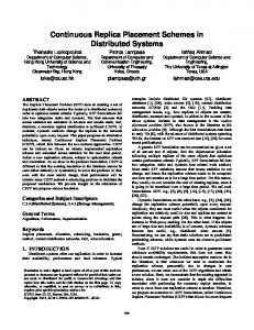
where α is the ratio of the minimum tolerable voltage across the terminals of a current load to the power supply voltage (α = 0.9 in this paper). If R1 > R1max , no solution exists for providing sufficient charge drawn by the load. In this case, the circuit block should be partitioned, reducing the current demands (Imax ). Note that expressions for determining the voltage across the decoupling capacitors are transcendental functions. No closed-form solution, therefore, exists. From (3) and (4), the design space can be graphically obtained for determining the maximum tolerable resistance R2 and the minimum magnitude of the capacitors, maintaining the voltage across the load equal to or greater than the minimum allowable level. The voltage across C1 after discharge as a function of C1 and R2 is depicted in Fig. 6. Observe from Fig. 6 that the voltage across capacitor C1 increases exponentially with capacitance, saturating for large C1 . The voltage across C1 , however, is almost independent
813
with larger R2 , as illustrated in Fig. 6(b). In general, to determine the parameters of the system of distributed on-chip decoupling capacitors, the following assumptions are made. The parasitic resistance of the metal line(s) connecting capacitor C1 to the current load is known. R1 is determined by technology constraints (the sheet resistance) and by design constraints (the maximum available metal resources). The minimum voltage level at the load is Vload = 0.9Vdd . The maximum magnitude of the current load Imax is 0.01 A, the rise time tr is 100 ps, and the power supply voltage Vdd is one volt. Note that the voltage across C2 after discharge as determined by (4) is also considered a design parameter. Since the capacitor C2 is connected directly to the power supply (a shared power rail), the voltage drop across C2 appears on the global power line, compromising the signal integrity of the overall system. The voltage across C2 at tr is therefore based on the maximum tolerable voltage fluctuations on the P/G line during discharge (the voltage across C2 at the end of the switching cycle is set to 0.95 volts). The system of equations to determine the parameters of an on-chip distributed decoupling capacitor network as depicted in Fig. 5 is
Voltage across C1, V
1 0.8
0.6
0.4
0.2
0 10 8
100 6
80 60
4
40
2
Capacitance C , pF
20 0
1
0
Resistance R2, Ω
(a)
5.5 5
Capacitance C1, pF
4.5 4
Vload V C1 V C2 Imax tr 2
3.5 3
C2 = C1
2.5 2
C = 2C 2
1.5
C = 4C 2
1 0
1
1
20
40
60
80
100
Resistance R2, Ω
(b) Fig. 6. Voltage across C1 during discharge as a function of C1 and R2 : Imax = 0.01 mA, Vdd = 1 volt, and tr = 100 ps. a) Assuming C1 = C2 and R1 = 10 Ω, the minimum tolerable voltage across C1 , resulting in Vload ≥ 0.9Vdd , is 0.91 volts (shown as a black equipotential line). b) The design space for determining C1 and R2 resulting in the voltage across C1 equal to 0.91 volts.
of R2 , decreasing slightly with R2 (see Fig. 6(a)). This behavior can be explained as follows. As a current load draws charge from the decoupling capacitors, the voltage across the capacitors drops below the initial level. The charge released by a capacitor is proportional to the capacitance and the voltage drop. A larger capacitance therefore results in a smaller voltage drop. From Fig. 5, note that as resistance R2 increases, capacitor C2 becomes less effective (a larger portion of the total current is provided by C1 ). As a result, the magnitude of C1 is increased to maintain the voltage across the load above the minimum tolerable level. Similarly, a larger C2 results in a smaller C1 . As C2 is increased, a larger portion of the total current is provided by C2 , reducing the magnitude of C1 . This phenomenon is well pronounced for small R2 , diminishing
= VC1 − Imax R1 , = f (C1 , C2 , R2 ), = f (C1 , C2 , R2 ),
(7) (8) (9)
= C1 (Vdd − VC1 ) + C2 (Vdd − VC2 ) , (10)
where VC1 and VC2 are the voltage across C1 and C2 and determined by (3) and (4), respectively. Equation (10) states that the total charge drawn by the current load is provided by C1 and C2 . Note that in the general case with the current load determined a priori, the total charge is the integral of Iload (t) from zero to tr . Solving (7) for VC1 and substituting into (8), C1 , C2 , and R2 are determined from (8) to (10), as discussed in the following section. IV. D ESIGN T RADEOFFS IN A D ISTRIBUTED O N -C HIP D ECOUPLING C APACITOR N ETWORK To design a system of distributed on-chip decoupling capacitors, the parasitic resistances and capacitances should be determined based on design and technology constraints. As shown in Section III, in a system composed of two decoupling capacitors (see Fig. 5) with known R1 , R2 , C1 , and C2 are determined from the system of equations, (7)–(10). Note that since this system of equations involves transcendental functions, a closed-form solution cannot be determined. To determine the system parameters, the system of equations, (7)– (10), is solved numerically [13]. Various tradeoff scenarios are discussed in this section. The dependence of the system parameters on R1 is presented in Section IV-A. The design of a distributed on-chip decoupling capacitor network with minimum magnitude C1 is discussed in Section IV-B.
814
TABLE II D ISTRIBUTED ON - CHIP DECOUPLING CAPACITOR NETWORK AS A FUNCTION OF R1 UNDER THE CONSTRAINT OF A MINIMUM C1
A. Dependence of System Parameters on R1 The parameters of a distributed on-chip decoupling capacitor network for typical values of R1 are listed in Table I. Note that the minimum magnitude of R2 exists for which the parameters of the system can be determined. If R2 is sufficiently small, the distributed decoupling capacitor network degenerates to a system with a single capacitor (where C1 and C2 are merged). For the parameters listed in Table I, the minimum magnitude of R2 is four ohms, as determined from numerical simulations.
VC2 �= const
R1
VC2 = 0.95 volt
(Ω)
R2 (Ω)
C2 (pF)
R2 (Ω)
C2 (pF)
R2 (Ω)
C2 (pF)
1 2 3 4 5
2 2 2 2 2
5.59 6.68 8.19 10.46 14.21
5 5 5 5 5
8.69 11.64 17.22 31.70 162.10
4.68 3.46 2.28 1.13 –
8.20 8.40 8.60 8.80 –
Vdd = 1 V, Vload = 0.9 V, tr = 100 ps, Imax = 0.01 A, and C1 = 1 pF
TABLE I D EPENDENCE OF THE PARAMETERS OF THE DISTRIBUTED ON - CHIP DECOUPLING CAPACITOR NETWORK ON R1 R2 = 5 (Ω)
R2 = 10 (Ω)
(Ω)
C1 (pF)
C2 (pF)
C1 (pF)
C2 (pF)
1 2 3 4 5
1.35 2.81 4.54 6.78 10.00
7.57 5.50 3.64 1.87 0
3.64 4.63 5.88 7.56 10.00
3.44 2.60 1.77 0.92 0
R1
Vdd = 1 V, Vload = 0.9 V, tr = 100 ps, and Imax = 0.01 A
Note that the parameters of a distributed on-chip decoupling capacitor network are determined by the parasitic resistance of the P/G line(s) connecting C1 to the current load. As R1 increases, the capacitor C1 increases substantially (see Table I). This increase in C1 is due to R1 becoming comparable to R2 , and C1 providing a greater portion of the total current. Alternatively, the system of distributed on-chip decoupling capacitors degenerates to a single oversized capacitor. The system of distributed on-chip decoupling capacitors should therefore be carefully designed. Since the distributed on-chip decoupling capacitor network is strongly dependent upon the first level of interconnection (R1 ), C1 should be placed as physically close as possible to the current load, reducing R1 . If such an allocation is not practically possible, the current load should be partitioned, permitting an efficient allocation of the distributed on-chip decoupling capacitors under specific technology constraints. B. Minimum C1 In practical applications, the size of C1 (the capacitor closest to the current load) is typically limited by technology constraints, such as the maximum capacitance density, and design constraints, such as the available area. The magnitude of the first capacitor in a distributed system is therefore typically small. In this section, the dependence of the distributed onchip decoupling capacitor network on R1 is determined for minimum C1 . A target magnitude of 1 pF is assumed for C1 . The parameters of a system of distributed on-chip decoupling capacitors as a function of R1 under the constraint of a minimum C1 are listed in Table II. Note that VC2 denotes the voltage across C2 after discharge.
Note that two scenarios are considered in Table II to evaluate the dependence of a distributed system of on-chip decoupling capacitors. In the first scenario, the distributed onchip decoupling capacitor network is designed to maintain the minimum tolerable voltage across the terminals of a current load. In this case, the magnitude of C2 increases with R1 , becoming impractically large for large R2 . In the second scenario, an additional constraint (the voltage across C2 ) is applied to reduce the voltage fluctuations on the shared P/G lines. In this case, as R1 increases, C2 slightly increases. In order to satisfy the constraint for VC2 , R2 should be significantly reduced for large values of R1 , meaning that the second capacitor should be placed close to the first capacitor. As R1 is further increased, R2 becomes negligible, implying that capacitors C1 and C2 should be merged to provide the required charge to the distant current load. V. C ASE S TUDY The dependence of the system of distributed on-chip decoupling capacitors on the current load and the parasitic impedance of the power delivery system is described in this section to quantitatively illustrate the previously presented concepts. The load is modeled as a ramp current source with a 100 ps rise time. The minimum tolerable voltage across the load terminals is 90% of the power supply level. The magnitude of the on-chip decoupling capacitors for various parasitic resistances of the metal lines connecting the capacitors to the current load is listed in Table III. The parameters of the distributed on-chip decoupling capacitor network listed in Table III are determined for two amplitudes of the current load. The parameters of the system of distributed on-chip decoupling capacitors are analytically determined from (7)– (10). The resulting power supply noise is estimated using SPICE and compared to the maximum tolerable level (the min ). The maxminimum voltage across the load terminals Vload imum voltage drop across C2 at the end of the switching . Note that activity is also estimated and compared to VCmin 2 the analytic solution produces accurate estimates of the onchip decoupling capacitors for typical parasitic resistances of a power distribution grid. The maximum error in this case study is 0.003%.
815
TABLE III T HE MAGNITUDE OF ON - CHIP DECOUPLING CAPACITORS AS A FUNCTION OF THE PARASITIC RESISTANCE OF THE POWER / GROUND LINES CONNECTING THE CAPACITORS TO THE CURRENT LOAD
R1
R2
Imax
C1
C2
(Ω)
(Ω)
(A)
(pF)
(pF)
min Vload
Vload (mV) SPICE
(%)
VCmin 2
SPICE
(%)
0.5 0.5 0.5 0.5 0.5 0.5 0.5 0.5 0.5 0.5 0.5 0.5 0.5 0.5 0.5 0.5 0.5 0.5
4.5 6 8 10 12 14 16 18 20 1.5 2 3 4 5 6 7 8 9
0.01 0.01 0.01 0.01 0.01 0.01 0.01 0.01 0.01 0.025 0.025 0.025 0.025 0.025 0.025 0.025 0.025 0.025
0 1.59747 2.64645 3.22455 3.59188 3.84641 4.03337 4.17658 4.28984 0 4.25092 7.97609 9.67473 10.65000 11.2838 11.72910 12.05910 12.31110
9.99999 6.96215 4.97091 3.87297 3.17521 2.69168 2.33650 2.06440 1.84922 24.99930 17.56070 11.04180 8.06921 6.36246 5.25330 4.47412 3.89653 3.44905
900 900 900 900 900 900 900 900 900 900 900 900 900 900 900 900 900 900
899.999 899.986 899.995 899.997 899.998 899.998 899.999 899.998 899.999 899.998 899.999 899.999 899.999 899.999 899.999 899.999 899.999 899.980
0.0001 0.002 0.0006 0.0003 0.0002 0.0002 0.0001 0.0002 0.0001 0.0002 0.0001 0.0001 0.0001 0.0001 0.0001 0.0001 0.0001 0.002
950 950 950 950 950 950 950 950 950 950 950 950 950 950 950 950 950 950
949.999 949.983 949.993 949.996 949.997 949.997 949.998 949.998 949.998 949.998 949.999 949.999 949.999 949.999 949.999 949.999 949.999 949.973
0.0001 0.002 0.0004 0.0004 0.0003 0.0003 0.0002 0.0002 0.0002 0.0002 0.0001 0.0001 0.0001 0.0001 0.0001 0.0001 0.0001 0.003
Error
VC2 (mV)
Error
Vdd = 1 V, and tr = 100 ps
From Table III, note that in the case of a large R2 , the distributed decoupling capacitor network degenerates to a system with a single capacitor. Capacitor C1 is therefore excessively large. Conversely, if C2 is placed close to C1 (R2 is small), C2 is excessively large and the system behaves 2 as a single capacitor. An optimal ratio R R1 therefore exists for specific characteristics of the current load that results in the minimum budgeted on-chip decoupling capacitance. Alternatively, in this case, both capacitors provide an equal portion of the total charge (see Table III for R1 = 0.5 Ω and R2 = 10 Ω). VI. C ONCLUSIONS A system of distributed on-chip decoupling capacitors has been proposed in this paper. A distributed on-chip decoupling capacitor network is an efficient solution for providing the required on-chip decoupling capacitance under existing technology constraints. In a system of distributed on-chip decoupling capacitors, each capacitor is sized based on the parasitic impedance of the power delivery system. Initially, the capacitor closest to the current load provides the required charge. Once the first capacitor is depleted, the next decoupling capacitor is activated, providing a large portion of the total current drawn by the load. This procedure is repeated until the last decoupling capacitor becomes active. Hierarchically allocating the on-chip decoupling capacitors greatly relaxes the technology constraints for physically distant capacitors, making the distant on-chip decoupling capacitors more effective. R EFERENCES
[2] M. Popovich and E. G. Friedman, “Impedance Characteristics of Decoupling Capacitors in Multi-Power Distribution Systems,” Proceedings of the IEEE International Conference on Electronics, Circuits and Systems, pp. 160–163, December 2004. [3] M. Popovich and E. G. Friedman, “Decoupling Capacitors for MultiVoltage Power Distribution Systems,” IEEE Transactions on Very Large Scale Integration (VLSI) Systems, Vol. 14, No. 3, pp. 217–228, March 2006. [4] A. V. Mezhiba and E. G. Friedman, “Scaling Trends of On-Chip Power Distribution Noise,” IEEE Transactions on Very Large Scale Integration (VLSI) Systems, Vol. 12, No. 4, pp. 386–394, April 2004. [5] M. Popovich and E. G. Friedman, “Noise Aware Decoupling Capacitors for Multi-Voltage Power Distribution Systems,” Proceedings of the IEEE International Symposium of Quality Electronic Design, pp. 334–339, March 2005. [6] M. Popovich, E. G. Friedman, M. Sotman, A. Kolodny, and R. M. Secareanu, “Maximum Effective Distance of On-Chip Decoupling Capacitors in Power Distribution Grids,” Proceedings of the ACM Great Lakes Symposium on VLSI, pp. 173–179, April/May 2006. [7] H. Su, S. S. Sapatnekar, and S. R. Nassif, “Optimal Decoupling Capacitor Sizing and Placement for Standard-Cell Layout Designs,” IEEE Transactions on Computer-Aided Design of Integrated Circuits and Systems, Vol. 22, No. 4, pp. 428–436, April 2003. [8] S. Zhao, K. Roy, and C.-K. Koh, “Decoupling Capacitance Allocation and Its Application to Power-Supply Noise-Aware Floorplanning,” IEEE Transactions on Computer-Aided Design of Integrated Circuits and Systems, Vol. 21, No. 1, pp. 81–92, January 2002. [9] J. Kim, et al., “Separated Role of On-Chip and On-PCB Decoupling Capacitors for Reduction of Radiated Emission on Printed Circuit Board,” Proceedings of the IEEE International Symposium on Electromagnetic Compatibility, pp. 531–536, August 2001. [10] T. Hubing, “Effective Strategies for Choosing and Locating Printed Circuit Board Decoupling Capacitors,” Proceedings of the IEEE International Symposium on Electromagnetic Compatibility, pp. 632–637, August 2005. [11] L. D. Smith, R. E. Anderson, D. W. Forehand, T. J. Pelc, and T. Roy, “Power Distribution System Design Methodology and Capacitor Selection for Modern CMOS Technology,” IEEE Transactions on Advanced Packaging, Vol. 22, No. 3, pp. 284–291, August 1999. [12] M. E. Van Valkenburg, Network Analysis, Prentice-Hall, 1974. [13] Mathematica 5.2, Wolfram Research, Inc.
[1] M. Popovich, A. V. Mezhiba, and E. G. Friedman, Power Distribution Networks with On-Chip Decoupling Capacitors, Springer Publishers, 2008 (in press).
816