Polymer 44 (2003) 6725–6760 www.elsevier.com/locate/polymer
Feature Article
Enabling nanotechnology with self assembled block copolymer patterns Cheolmin Parka, Jongseung Yoonb, Edwin L. Thomasb,c,* b
a Department of Metallurgical System Engineering, Yonsei University, Seoul 120-749, South Korea Department of Materials Science and Engineering, Massachusetts Institute of Technology, Cambridge, MA 02139, USA c Institute for Soldier Nanotechnologies, Massachusetts Institute of Technology, Cambridge, MA 02139, USA
Accepted as submitted 29 July 2003
Abstract Block copolymers (BCPs) have received great attention for the past 40 years but only within the past decade have they been seriously considered for nanotechnological applications. Their applicability to nanotechnology stems from the scale of the microdomains and the convenient tunability of size, shape, and periodicity afforded by changing their molecular parameters. The use of the tensorial physical properties of BCPs in such areas as transport, mechanical, electrical, and optical properties will provide substantial benefits in the future. In this review article, we first focus on the current efforts to utilize BCPs in nanotechnologies including nanostructured membranes, BCP templates for nanoparticle synthesis, photonic crystals, and high-density information storage media. In order to realize these applications, control over microdomain spatial and orientational order is paramount. This article reviews various methods to control BCP microdomain structures in the bulk state as well as in thin films. A variety of biases such as mechanical flow fields, electric fields, temperature gradients, and surface interactions can manipulate the microstructures of BCPs. A particular emphasis is made on two approaches, epitaxy and graphoepitaxy, and their combinations. Manipulation of BCP microdomain structures employing multiple external fields promises realization of many potential nanotechnological applications. q 2003 Elsevier Ltd. All rights reserved. Keywords: Block copolymers; Self-assembly; Nanostructures
1. Introduction Nanometer scale patterns based on self assembly have been considered as alternatives to replace or augment high resolution lithographic technologies such as X-ray, electron beam and interference lithography to enable a variety of nanotechnologies. In particular, block copolymers (BCPs) have recently received much attention not only thanks to the scale of the microdomains (tens of nanometers), their various chemical and physical properties (e.g. differential etching rates) but also due to the convenient size and shape tunability of microdomains afforded by simply changing their molecular weights and compositions. Many potential uses of BCPs for different nanotechnologies have been proposed based on principally their ability to form interesting patterns. However, the main challenge of * Corresponding author. Address: Department of Materials Science and Engineering, Massachusetts Institute of Technology, Room 13-5094 77 Massachusetts Avenue, Cambridge, MA 02139, USA. Tel.: þ 1-617-2535931; fax: þ 1-617-253-5859. E-mail address:
[email protected] (E.L. Thomas). 0032-3861/$ - see front matter q 2003 Elsevier Ltd. All rights reserved. doi:10.1016/j.polymer.2003.08.011
using BCPs lies with control of microstructure. Achievement of precise microdomain location, orientation, and elimination of various defects requires introduction of external fields during the processing step. A variety of mechanical, electrical, magnetic biases and surface interactions have been proposed to manipulate and guide the microstructures of BCPs. In this article we point out examples of potential applications using self assembled BCPs particularly focused on nanotechnology. We extensively review various methods to control microdomain structures of BCPs in the bulk state as well as in thin films, which are requisite for facilitating many industrial applications. A particular emphasis is made on two processing approaches: epitaxy (and directional crystallization of a solvent), and graphoepitaxy as well as their combinations. Epitaxy is defined as the growth of a crystal of one phase on the surface of that of another phase in one or more strictly defined crystallographic orientations [1 –3]. Epitaxy between a crystalline block and a crystalline substrate whereby a crystallizable organic solvent (such as benzoic acid) serves as a solvent for a semicrystalline BCP
6726
C. Park et al. / Polymer 44 (2003) 6725–6760
at temperatures above the solvent melting temperature and becomes a substrate onto which the crystallizable block can orient when the block is cooled below the solvent’s melting point is shown to be an excellent way to form highly aligned edge-on crystalline lamellae in both lamellar and cylindrical microdomains formed from semicrystalline – amorphous BCPs. Graphoepitaxy is a process in which an artificial topographic surface pattern is employed to control orientation of crystal growth in thin films [4,5]. When a topographically patterned substrate is utilized to template the self-assembly of a BCP thin film, well-aligned structures of BCP microdomains are obtained due to controlled confinement. The directional crystallization process when applied to a crystallizable solvent can induce an overall orientation of the BCP inter-material dividing surface (IMDS) parallel to the temperature gradient [6]. When a BCP which contains a crystallizable block is used, one can also utilize epitaxy in combination with directional crystallization to control the microdomain pattern. Furthermore, when directional crystallization is used in combination with graphoepitaxy, where the process is conducted on a film confined to have various thicknesses using the topographically patterned substrate, two types of microdomain orientation can be accessed (Sections 3.4 and 3.5) To illustrate the usefulness of the self assembled BCP approach to nanotechnology, we highlight several applications where the microdomain patterns obtained via self assembly in a bias field are critical to the technology. First, we turn to a brief review of alternative methods of pattern formation in nanotechnology (‘top – down’ approaches). 1.1. Patterning methods other than self assembly (‘top –down’ methods) Fabrication of precisely ordered nanoscale structures is essential for nanotechnology. The ability to fabricate on the nanometer scale guarantees a continuation in the miniaturization of functional devices and the large inherent surface/volume ratio, short diffusion distances etc. offer advantages over micro- and macroscale devices. New advanced fabrication technologies have enabled the lateral dimensions of devices to be shrunk well below 100 nm. Lithography dominates as the most critical procedure for successfully defining structures with such dimensions. Photo-lithographic methods all share the same operational principle [7]. Exposure of an appropriate material to electromagnetic radiation (ultra violet (UV), deep ultra violet (DUV) or X-ray) introduces a latent image (usually a difference in solubility) into the material as a result of a set of chemical changes in its molecular structure; This latent image is subsequently developed into 1D or 2D relief structures through selective etching. X-ray lithography has been used to create submicron size features [8]. Moreover, interference lithography, using interactions between two or more coherent laser beams, and zone-plate array lithography in which array of Fresnel zone plates focus the X-ray beam
source and directly pattern on the resist surface without a mask, have been developed to create submicron features in an inexpensive way [9,10]. Recently, four beam interference lithography was used for production of 3D photonic crystals in the visible wavelength regime [11]. A near-field scanning optical microscope (NSOM) was also employed as a photolithographic tool on the submicron length scale. This technique is not diffraction limited and can be used to generate a smaller feature size than those achieved by far-field photolithography [12]. Methods based on writing with charged particles (electrons or ions) usually accomplish the same task using a scanned beam or projected image of energetic particles rather than photons [13 – 19]. Exposure is usually patterned either by interposing a mask between the source of radiation and the material or by scanning a focused spot of the source across the surface of the material. When masks are used, the lithographic process yields a 2D replica of the pattern on the mask. Focused ion beam lithography (FIB) [13,14] and electron beam lithography [15 – 19] are both well suited for generating patterns on the submicron scale. A shadow-mask evaporation or ‘nanostencil’ method has also been used to define submicron single layer material patterns [20]. In this approach, the nanostencil, a perforated ultra-thin silicon nitride membrane with various submicron size apertures, is in contact with the substrate surface during deposition. The combination of shadow mask (nanostencil) and scanning probe methods such as atomic force microscope (AFM) and scanning tunneling microscope (STM) provide improved manipulation of the pattern structures. With scanning probes, a sharp tip (, 50 nm) induces a local change in a resist or causes localized deposition of a material. Methods that involve scanning or writing can generate arbitrary 2D patterns and therefore can be used for master writing. Advantages of scanning probe methods include resolution that, for AFM and STM methods, approaches the atomic level, the ability to generate features with nearly arbitrary geometries, and the capability to pattern over surface topography that deviates significantly from planarity [21]. These methods are serial techniques, however, and have writing speeds that are typically limited by the mechanical resonances of the tips and the piezoelectric elements that maintain constant separation between the tip and the sample surface. Direct patterning on self assembled monolayers (SAMs) using an AFM was developed to study selective protein adsorption on patterned areas. The method, called nanografting, combined the displacement of selected resist molecules by an AFM tip and the adsorption of new adsorbate [22,23]. Nanografting allows a more precise control over the size and geometry of patterned features and their locations on surfaces. Another technology using a scanning probe is dip-pen nanolithography (DPN) [24,25]. DPN uses an AFM tip as a ‘nib’, a solid-state substrate (in this case, Au) as ‘paper’, and molecules with a chemical affinity for the solid-state
C. Park et al. / Polymer 44 (2003) 6725–6760
substrate as ‘ink’. Capillary transport of molecules from the AFM tip to the solid substrate is used in DPN to directly ‘write’ patterns consisting of a relatively small collection of molecules in submicrometer dimensions. However, this method also patterns the substrate sequentially, and therefore the patterning time scales linearly with the area to be patterned. An alternative high-throughput lithographic method is nanoimprint lithography (NIL), where patterns are defined by a compression molding and a pattern transfer [26]. In this approach, a mold having nanometer length-scale features is first compressed onto a thin resist film deposited on a substrate. A thickness contrast created in the molded resist enables an anisotropic etching process and pattern transfer. The characteristics of various top – down nanolithographic techniques mentioned above are summarized in Table 1. 1.2. Self assembly methods (‘bottom – up’ methods) These patterning methods just described usually require expensive equipment and/or long writing times. Another approach is to use ‘self assembly’ to create patterns via a ‘bottom – up approach’. Nature uses self-assembling materials for nanostructures such as the components for living cells [27]. Most biological systems also exhibit hierarchy and at least one distinct structural feature that lies within each length scale at the molecular, nanoscopic, microscopic and macroscopic regimes. Several levels of
6727
structure can be distinguished in proteins, bones and shells [28]. For example, in proteins, the primary structure of the sequence of amino acid groups along the polypeptide chain is developed into various secondary structural motifs, such as coils, sheets and ribbons. The motifs are in turn packed together to give the overall molecule a distinctive shape, the tertiary structure. The association of several subtertiary units corresponds to the protein’s quaternary structure. Many other examples of self assembly of biomaterials can be found, for instance, in tobacco mosaic virus which is a self-assembling replication machine [28]. Human attempts at similar structures are, at present, limited to building self-assembling nanoscale materials a few atoms or molecules at a time. The field of biomimetics is based on the supposition that nature can provide models for processing at the submicrometer scale. Artificial nanoscale structures can be fabricated with similarity to biological materials, through the application of self assembly coupled with lamination and directed patterning methods. Various examples can be observed in biology, in the field of embryology and morphogenesis [27]; in chemistry, where groups of molecules form supramolecular structures [29,30]. Artificial peptides or proteins can be engineered to achieve potentially useful nanostructures. For example, Tirrell et al. synthesized triple-stranded b-sheet peptides designed for an ordered 2D molecular assembly at the air -water interface [30]. In materials science, various colloid particles have been made for self assembly [31,32],
Table 1 Characteristics of top–down nanometer scale patterning techniques Technique
Minimum resolution (nm)
Source materials
Nature of patterns
Intrinsic limitations
Advantages
References
UV photo lithography X-ray lithography Interference lithography
250 25 .100
248 nm KrF excimer laser Soft X-ray with near 1nm Holographic interactions between two or more lasers Fresnel zone plates X-ray beam UV or VIS laser with fiber optic probe Focused ion beam
2D 2D 2D, 3D
Easy replication Easy replication No mask easy replication
[7] [8] [9,11]
2D
Diffraction depth of focus Diffraction depth of focus Diffraction depth of focus limited patterns Zone plate fabrication
No mask
[10]
2D
Serial patterning
No diffraction limit
[12]
2D
Writing pattern
[13,14]
Focused electron beam
2D
Electrostatic interactions serial writing small field writing Electrostatic interactions serial writing small field writing Serial patterning limited writing speed
Writing pattern
[15–19]
Zone plate array .100 lithography Near-field scanning optical ,100 lithography Focused ion beam ,50 lithography Electron beam lithography
10–30
Nanografting
5–50
Modified AFM tip
2D
Dip-pen lithography
5–50
Modified AFM tip
2D
Nano imprint lithography
10–40
Stamp and polymeric resist 2D
High resolution arbitrary [22,23] geometries chemical patterns Serial patterning limited High resolution arbitrary [24,25] writing speed geometries chemical patterns Fabrication of stamp multi- High resolution large area [26] step process alignment printing relatively low cost fidelity
6728
C. Park et al. / Polymer 44 (2003) 6725–6760
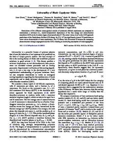
Fig. 1. (a) Schematic phase diagram showing the various ‘classical’ BCP morphologies adopted by non-crystalline linear diblock copolymer. The blue component represents the minority phase and the matrix, majority phase surrounds it. (b) Schematic of morphologies for linear ABC triblock copolymer. A combination of block sequence (ABC, ACB, BAC), composition and block molecular weights provides an enormous parameter space for the creation of new morphologies. Microdomains are colored as shown by the copolymer strand at the top, with monomer types A, B and C confined to regions colored blue, red and green, respectively. (Reprinted with permission from Physics Today [39]. Copyright (1999) American Institute of Physics).
and organic polymers were synthesized on inorganic surfaces [33]. In achieving nanostructures and nanoelectronic devices, chemical self-assembly has become an important factor in building supramolecular nanopattern structures. 1.3. Block copolymers self assembly BCPs satisfy the size requirement for many potential nanotechnologies [34,35] and are an example of chemically
directed self assembly. BCPs consist of chemically distinct polymer chains covalently linked to form a single molecule. Owing to their mutual repulsion, dissimilar blocks tend to segregate into different domains, the spatial extent of the domains being limited by the constraint imposed by the chemical connectivity of the blocks. Area minimization at the interface (the IMDS) of two blocks takes place to lower the interfacial energy. From an entropic standpoint, the molecules prefer random coil shapes but the blocks are stretched away from the IMDS to avoid unfavorable
C. Park et al. / Polymer 44 (2003) 6725–6760
6729
Fig. 2. SEM micrographs showing a bicontinuous nanochannel in the matrix of PS with two different magnifications ((a), (b)) and computer graphics of a double gyroid network: (c) a 3D view and (d) a 2D intersection cut along the (211) direction. (c) shows a solid model in which only the matrix phase, corresponding to the PS matrix in our specimens, is shown. In (d), the bright domain corresponds to the PS matrix and the gray and dark phases correspond to the degraded PI phase. (Reprinted with permission from Langmuir [42]. Copyright (1997) American Chemical Society).
contacts. As a result, of these competing effects, selforganized periodic microstructures emerge on the nanoscopic length scale. Various microdomain structures are achieved, depending on relative volume ratio between blocks and chain architecture as well as the persistence lengths of the respective blocks. In the simplest case of non-crystalline flexible coil AB diblock copolymers, the composition of the AB diblock (i.e. the volume fraction f of block A) controls the geometry of the microdomain structure. As shown in Fig. 1(a), for nearly symmetric diblocks ðf , 1=2Þ; a lamellar (LAM) phase occurs. For moderate compositional asymmetries, a complex bicontinuous state, known as the double gyroid (DG) phase, has been observed in which the minority blocks form domains consisting of two interweaving threefoldcoordinated networks. At yet higher compositional asymmetry, the minority component forms hexagonally packed cylinders (CYL) and then spheres (SPH) arranged on a body-centered cubic lattice. Eventually, as f ! 0 or 1, a homogeneous phase results [36]. The equilibrium morphologies of ABC triblock terpolymers are more diverse than those of AB diblock copolymers (Fig. 1(b)) [38]. In ABC triblock terpolymers, there exist two composition
variables and three interaction parameters, which make their phase behaviors much more complicated than AB diblocks having only one composition variable and one interaction parameter [39]. More extensive information regarding morphologies of complex BCP systems including ABC triblocks and star copolymers can be found in other literature [40,41]. 1.4. Nanotechnologies with BCPs In the next several sections we outline some potential nanotechnological applications enabled with BCPs. Until recently, most industrial applications of BCPs were as adhesives or for their mechanical properties (e.g. as thermoplastic elastomers). Only in the past 10 years have researchers taken BCPs into the ‘high-technology’ area, to the so-called ‘nanotechnologies’. Many attempts have been made to utilize BCPs in nanotechnology. This section focuses on various uses of BCPs in the solid state. Applications of BCP solutions, such as micelles for drug delivery, are not covered in this article. For more detailed and extensive information, the readers can refer to other literature [35,37,38]. Self assembled BCP microstructures
6730
C. Park et al. / Polymer 44 (2003) 6725–6760
with 10 to 100 nm dimensions are useful as nanometer scale membranes, templates for fabrication of nano-objects such as metal, ceramic nanodots and wires, as 1-, 2- and 3D photonic crystals, and as nanopattern masks for fabrication of high density information storage media. The key features needed for each application and the previous efforts to attain these nanotechnological functions are described next section. 1.4.1. Nanostructured networks and membranes BCPs can be utilized as precursor materials for the fabrication of nanostructured networks and membranes by choosing properly designed block chemistries, microdomain phases and processes. Hashimoto et al. first produced nanometer length scale channels in a bicontinuous DG microdomain structure formed by blending poly (styrene-b-isoprene) (PS/PI) diblock copolymer and polystyrene homopolymer [42] to achieve the correct overall PS matrix volume fraction. The minor domain polyisoprene networks were selectively removed using ozonolysis and the nanochannel surface was plated with nickel metal for catalytic applications (Fig. 2). The need for low k materials in microelectronics suggested formation of a nanoporous silica material via ozonolysis of a silicon containing BCP precursor [43,44]. A membrane with nanoporous channels was fabricated by cross-linking of the silyl containing block and by selective ozone etching of the network forming polydiene block in a silyl containing BCP [44]. A self-assembled DG nanorelief structure was developed from spin casting, annealing and ozonolysis of the matrix to create a nanoscale bicontinuous ceramic (SiO2) network structure [43]. Such materials offer very large surface/volume ratio, low density and their nanoporous or nanorelief structures are advantageous for photonic and membrane applications. Mesostructured silicates have been prepared through the use of BCPs as structure-directing agents [45 –49]. The processing of sol – gel ceramics with BCPs is similar to that using surfactant molecules but gives structures at a larger length scale. For example, mesoporous silica films have been fabricated using amphiphilic BCPs as the structure directing agent (Fig. 3) [45 – 49]. The aqueous silica cations partition within the hydrophilic regions of the selfassembled system and subsequent sol – gel polymerization of the silica precursor produces a densely cross-linked silica network precisely templating the original microphase separated BCP structure. Mesoporous ceramic materials were obtained via heat treatment of a BCP/silicate composite while discrete nano-objects with controlled shape, size, and compositions were made via selective solvent swelling of hydrophobic phase in the composite (Fig. 4) [48,49]. BCP-directed silicate structures have been utilized for fabricating an optical waveguide which in combination with a laser dye, can efficiently self-lase [50]. An approach that is more obviously biomimetic uses synthetic cysteine – lysine block ‘copolypeptides’ that mimic the properties of
Fig. 3. TEM micrographs of the 62 wt% poly(ethylene oxide-b-propylene oxide-b-ethylene oxide)/SiO2 (EO106 – PO70 – EO106/SiO2) transparent composite revealing (a) a well-ordered hexagonal array of cylindrical aggregates viewed end-on and (b) hexagonal arrays of aggregates viewed from the side. Regions in the sample that are predominantly organic appear light, in contrast to the darker silica. Note the scale bars are different for the two images. (Reprinted with permission from Macromolecules [47]. Copyright (1999) American Chemical Society).
silicatein, a protein found to direct silica growth in certain sponges [51]. The morphology of the silica mesostructure, i.e. spheres and columns of amorphous silica, is controlled by using the reduced and the oxidized forms of the copolymer, respectively. 1.4.2. Nanoparticle templates BCPs have also been utilized not only as surfactants to inhibit coalescence and aid in dispersion of nanoscale particles such as metal, metal oxide, inorganics, molecular chromophores and quantum dots but also to spatially pattern the particles [52 –69]. The selective dispersion of quantum dots into a target set of microdomains within functionalized polynorbornene BCPs was first achieved by controlling the affinity between the selective block and quantum dot surface (Fig. 5(a)) [56,57]. A photonic crystal with improved dielectric contrast was made by selective deposition of CdSe nanocrystals to the 2-vinyl pyridine (2VP) microdomains of a self-assembled poly(styrene-b-isoprene-b-2-vinyl pyridine) triblock copolymer (Fig. 5(b)) [71]. In another
C. Park et al. / Polymer 44 (2003) 6725–6760
6731
Fig. 4. Schematic drawing for the preparation of nano-objects as well as mesoporous materials. Single ‘hairy’ nano-objects of different shapes are isolated by dissolution. Calcination at about 600 8C lead to mesoporous materials. (Reprinted with permission from Chem Mater [49]. Copyright (2001) American Chemical Society).
approach to patterning nanoparticles with BCPs, the BCP domain structure has been used as a ‘nano-reactor’ where nanoscale particles are induced to nucleate and grow through the chemical reactions [52 – 55,58,61 – 65]. For example, nanometer scale platinum and palladium catalysts were generated and stabilized within the polystyrene core of poly(styrene-b-ethylene oxide) BCP spherical domains [58]. Electroless deposition of metals into selected microdomains has been recently performed to provide continuous material loading [42,62,63]. The tendency of selective adsorption of metals in BCPs has also been used. Gold nanoparticles were selectively patterned on the cylinderforming poly(styrene-b-methylmethacrylate) (PS/PMMA) BCP thin film via thermal evaporation [67]. Recently, Bockstaller et al. demonstrated a hierarchically patterned microstructure of ternary mixtures of two different-sized nanoparticle species (gold and silica) and a BCP by strategic design of the size and the respective surface coatings of the nanoparticles (Fig. 5(c)) [68,69]. The authors also showed that a homogeneous sequestering of nanocrystals into selfassembled BCP is a more advantageous morphology than interfacial segregation and center alignment of nanocrystals for engineering block copolymer based photonic materials with high reflectivity since it allows one to incorporate a larger amount of nanocrystals while preventing enhanced light absorption by the electrodynamic coupling effect between neighboring metallic nanocrystals [69]. 1.4.3. Photonic crystals BCPs have recently been utilized to develop periodic self
assembled photonic band gap materials [70 –80]. The first example was a simple 1D photonic crystal made with high molecular weight lamellar forming BCP (Fig. 6(a)) [70 –72]. The alternating layer stack in the BCP lamellar structure is readily formed by self assembly in between two glass substrates and shows a nearly perfect normal incidence photonic band gap property. Variation of the microdomain thickness was accomplished by blending homopolymers into their respective microdomains, leading to tunability of the photonic band gap across the entire visible spectrum [73]. Photonic band gap materials based on BCPs have inherently low dielectric contrast. Thus, selective addition of nanoparticles to BCPs can tailor the effective dielectric constant of the targeted microdomain [78]. Selective dispersion of metallic gold nanoparticles into BCP microdomains enabled the creation of a lamellar type nanocomposite which revealed metallodielectric photonic crystal behavior [74]. A 2D photonic crystal that exhibits a partial bandgap in the visible regime was fabricated via roll casting (Section 2.1.3) a cylinder-forming poly(styrene-b-isoprene) (PS/PI) BCP (Fig. 6(b)) [75]. The bicontinuous DG cubic microstructure was also employed for 3D photonic application where selective removal of the PI matrix by an UV etching treatment of the PS/PI diblock improved the dielectric contrast in the bicontinuous PS/air structure, resulting in a photonic crystal with a more robust partial photonic band gap at visible wavelengths (Fig. 6(c)) [76]. A thermally tunable photonic band gap material has been fabricated by selectively incorporating liquid crystals into a BCP. Hydrogen bonding was used to attach the liquid
6732
C. Park et al. / Polymer 44 (2003) 6725–6760
crystal mesogens onto the backbone of the poly(styrene-bmethacrylic acid) BCP. The hierarchically structured, hybrid material could be switched from a green to an orange reflector by heating the LC block into the isotropic state [80]. In order to guide experiments and confirm the optical properties, theoretical calculation of the band structures of 3D bi- and tricontinuous cubic structures has been also done using the plane-wave method using a level set approach to define the various 3D network geometries [77,81].
˚ CdSe nanoclusters in a thin film Fig. 5. (a) TEM micrograph of 45 A of diblock copolymer of phosphine oxide functionalized monomers (NBE-CH2O(CH2)5P(oct)2 and methyltetracyclododecene (MTD), slowcast after 30 min equilibration time. (Reprinted with permission from Macromolecules [57]. Copyright (1997) American Chemical Society) (b) TEM micrograph of 1D self-assembled dielectric lattice made of poly(isoprene-b-2vinyl pyridine-b-isoprene) (PI/P2VP/PI) with TOPO coated CdSe nanocrystals sequestered in the 2VP phase. (Reprinted with permission from J. Lightwave Tech. [71]. Copyright (1997) The Institute of Electrical and Electronics Engineers) (c) TEM micrograph of a ternary blend of PS-PEP þ AuR1 þ SiO2R2 with inorganic filling fraction
1.4.4. Block copolymer masks for nanolithography The periodic nanostructures of BCPs are very useful in thin films as masks for nanolithography [82 – 94]. Mansky et al. [82,83] first demonstrated monolayer films of diblock copolymer microdomains could potentially be used as masks for nanolithography, on the scale of a few tens of nanometers. For both cylinder- and sphere-forming poly (styrene-b-butadiene) (PS/PB) diblock copolymers, grains measuring typically 30 £ 30 lattice constants were readily obtained [83]. Using spin-coated BCP thin films of wellordered spherical or cylindrical microdomains as the etching mask, dense, periodic arrays of holes and troughs have been fabricated in silicon, silicon nitride, and germanium. Domains approximately 20 nm wide, 20 nm deep, and spaced 40 nm apart, yielding a pattern with 5 £ 1011 holes/ cm2 were obtained on a three inch wafer [86]. In addition, GaAs nanoparticles have been grown in a hexagonally ordered array of nanometer scale holes with a density as high as , 1011/cm2 by metal-organic chemical vapor deposition [88]. Insertion of a polyimide layer underneath a sphere forming BCP thin film allowed fabrication of a high aspect ratio mask for nanolithography [89]. Recently, Ober et al. have introduced high resolution photoresist chemistry into BCPs based on hydroxy styrene. These polymers have been successfully patterned as negative tone resists with image sizes as small as 400 nm. It was possible to remove via UV exposure of the second minority phase consisting of alpha-methyl styrene to create a porous film with a 20 nm substructure [90]. Ultra high density storage media can be made by transferring a simple 2D periodic BCP pattern into a magnetic film substrate (see also Section 3.3 for a commercial application). For example, a BCP-hard mask-magnetic layer scheme was recently introduced for creating patterns of magnetic particles (Fig. 7(a) – (d)) [91,92]. The BCP lithographic mask was created by reactive ion etching (RIE) of a PFS-sphere-forming poly(styrene-b-ferrocenyldimethylsilane) (PS/PFS) diblock copolymer film in an f ¼ 0:02; respectively, after micro-sectioning normal to the layer direction (no stain). Gold nanocrystals appear as dark spots along the IMDS, silica nanocrystals reside in the center of the PEP domain. Inset: Schematic of the particle distribution (size proportions are changed for clarity). (Reprinted with permission from J. Am. Chem. Soc. [68]. Copyright (2003) American Chemical Society).
C. Park et al. / Polymer 44 (2003) 6725–6760
6733
Fig. 6. (a) SEM backscattered electron intensity image collected from a lamellar-forming poly(styrene-b-isoprene) (PS/PI) BCP stained with OsO4. (Reprinted with permission from Adv Mater [73]. WILEY-VCH, STM-Copyright & Licenses (2000)) (b) Reflectance spectra of a 17% by weight in toluene a lamellarforming PS/PI BCP solution. The width of this reflective peak is about 6 nm, indicating that the index contrast between the two phases is low. (c) Phase mode AFM image of a cylinder forming PS/PI BCP oriented by roll casting. The cylindrical microdomains of PS have higher modulus than PI matrix and are shown as white spots. (d) Reflectance spectra of (c) shows a strong reflectance over the wavelength range of 390 –440 nm. The film showed almost zero-transmission at the wavelength of maximum reflectance. (e) SEM secondary electron image of the double gyroid styrene networks remaining after UV/ozone etching of PI
6734
C. Park et al. / Polymer 44 (2003) 6725–6760
Fig. 7. Tilted SEM micrographs of the fabrication process of Co dot array using PS-PFS BCPs. (a) An O2-RIE treated block copolymer thin film on a multilayer of silica, the metallic films and the silicon substrate. (b) Pillars of silicon oxide capped with oxidized PFS after CHF3-RIE. (c) W (tungsten) hard mask on top of a Co layer. (d) Co dot array produced Ne ion-beam etching. (Reprinted with permission from Adv Mater [91]. WILEY-VCH, STM-Copyright & Licenses (2001)).
oxygen plasma (Fig. 7(a)), where because the PFS block contains both iron and silicon, upon oxidation the PFS forms a silicon –iron oxide providing excellent etching contrast (, 1:10) compared to PS matrix. One set of domains of the BCP was selectively removed to create the nanopatterned structure (Fig. 7(b)) and the pattern was subsequently transferred into the tungsten hard mask used for better surface adhesion among the layers (Fig. 7(c)). A subsequent ion milling process transferred the pattern structure of the
hard mask into a magnetic layer and developed the nanoscale magnetic pattern structure (Fig. 7(d)). The resulting cobalt dots were small enough for single domain magnetic particles and have an areal density of 3 £ 108 dots/ cm2. The experimental coercivity of these patterned magnetic dots arrays can be contributed to in-plane shape anisotropy as well as non-zero crystalline anisotropy. Thurn-Albrecht et al. have recently demonstrated a way to fabricate a high density ferromagnetic cobalt nanowire
domain in double gyroid forming PS/PI BCP. (Reprinted with permission from Adv Mater [76]. WILEY-VCH, STM-Copyright & Licenses (2002)) (f) Reflectivity spectra of (e) collected from 200 to 800 nm that shows features characteristic of the double gyroid structure for both the unetched styrene/isoprene material, and the UV-etched material. The first three allowed Bragg reflections are indicated with arrows, and are present in both reflection spectra. Bragg diffraction with an effective index is more reliable for the unetched structure, at high index contrast it is harder to justify its use. In addition, strong absorption by the polymer of wavelengths below 300 nm may be influencing the reflectivity spectra. (Reprinted with permission from Adv Mater [76]. WILEY-VCH, STM-Copyright & Licenses (2002)).
C. Park et al. / Polymer 44 (2003) 6725–6760
6735
Table 2 Characteristics of nanotechnologies enabled with BCPs
Fig. 8. Schematic drawing of process flow for MOS capacitors. (a) Polymer template formation on silicon surface. (b) RIE pattern transfer of PS template into silicon, followed by the removal of the PS matrix. (c) SiO2 growth followed by top Al gate electrode deposition. (d) a SEM image at a 708 tilt after RIE etch. Top shows remaining PS template. Bottom shows nanoscale hexagonal array has been transferred into Si counter electrode (Reprinted with permission from Appl Phys Lett [94]. Copyright (2001) American Institute of Physics).
structure with the density as high as 1.9 £ 1011 wires/cm2 using a BCP template [93]. Enhanced coercivities were observed, proposing another route to ultrahigh density storage media. Thin film nanolithography on a silicon substrate using a cylinder-forming PS/PMMA BCP as a mask in combination with standard semiconductor processing techniques produced a semiconductor capacitor. Silicon dioxide and aluminum gate electrodes were thermally grown on the patterned silicon substrate enabling a Metal-oxide –semiconductor capacitor to be fabricated exhibiting increased charge storage capacity (Fig. 8) [94]. Furthermore, a potential display device application for side chain ferroelectric liquid crystalline polymer films has been considered (Fig. 9) [95]. Mao et al. synthesized a side chain liquid crystal BCP with a ferroelectric smectic Cp liquid crystal block [96]. They found unwinding of the helical precession of the dipoles in a chiral smectic liquid crystal permits bistable field switching. This is normally done via confinement of the LC material between rubbed electrodes having a small gap. The concept of using the multiple IMDS between a microphase separated smectic Cp block-coil diblock lamellar copolymer was shown to unwind the helix. In this case the thin film geometry aligned the lamellar layers
6736
C. Park et al. / Polymer 44 (2003) 6725–6760
Fig. 9. Schematic of a surface stabilized ferroelectric LC display. (Reprinted with permission from Science [95]. Copyright (1996) The American Association for the Advancement of Science).
and poling in the applied electric field aligned the smectic LC layers and the IMDS prevented helical coupling across the material [96]. The characteristics of various BCP enabled nanotechnologies mentioned above are summarized in Table 2. 1.5. Limitations and opportunities The chief limitation to using BCPs to form periodic patterns for various nanotechnological applications lies with the fact that while the self assembled structure is locally very precise it is hard to control the order on the global scale. Indeed, the microdomains composed of the different blocks, having sizes of several tens of nanometers, typically nucleate randomly and grow as a polygranular texture, with periodic ordering maintained only over distances of several tens of lattice constant (i.e. a typical grain size of only
1 , 2 mm). For example, Fig. 10 shows a bright field TEM micrograph of a lamellar-forming poly(butadiene-bstyrene) (PB/PS) BCP thin film prepared on a carbon film by solvent evaporation [207]. The PS microdomains appear bright due to the selective OsO4 staining of the PB blocks. Besides many dislocation defects, the sample exhibits terracing. The lamellar microdomains are seen perpendicular to the film surface. In spite of a regular domain size, the poor long-range order and height variation greatly restricts the use of such patterns for many nanotechnological applications. A greater range of engineering applications demand control over both the orientation, the position of the microdomains and the film thickness. Several techniques are currently used for inducing longrange order of the microdomains in BCP. They rely on the ability to couple an externally applied field or surface pattern to some molecular and/or supermolecular feature in the polymer, and thus achieve anisotropic properties, such as transport, electrical, optical and mechanical properties. In the next section, we review various approaches to control the microstructures of BCP thin films that are essential to realize these potential nanotechnologies. We emphasize recent contributions to this area using surface matching (epitaxy), confinement (graphoepitaxy) and directional crystallization of a solvent.
2. Organization of block copolymer microdomains
Fig. 10. TEM micrograph of an unannealed sample of lamellar-forming poly(butadiene-b-styrene) (PB/PS) BCP, where the lamellae are seen perpendicular to the film surface. Many dislocation defects and a terracing formation are observed.
The role of BCPs in nanotechnologies will be much more significant if the full tensorial physical properties of highly ordered BCPs can be accessed. Control over microdomain orientation(s) and elimination/minimization of defects plays a crucial role for optimization of the resultant physical properties of the nanostructures. Understanding the mechanism of defect formation has been an essential topic in controlling BCP microstructures. The type of defects occurring in BCPs is dictated by the symmetry of the particular microdomain pattern of the particular BCP [97]. In general, point, line and surface defects occur just as in other ordered media (i.e. liquid
C. Park et al. / Polymer 44 (2003) 6725–6760
Fig. 11. TEM micrograph of an osmium tetroxide stained poly(isoprene-bpentamethyldisilylstyrene-b-isoprene) triblock copolymer with a volume fraction of 34% polyisoprene. Tilt grain boundary in a cylindrical microdomain viewed along the [0001] direction is observed, where two grains of hexagonally packed cylinders meet at grain boundary. Each of these layer cylinders has seven nearest neighbors (arrow a) or five nearest neighbors (arrow b), compared to 6 nearest neighbors for cylinders within the grains.
crystals, crystals). The size scale of the defects is set by that of the domain periodicity, and their energetics depend on the particular defect type as well as the inherent physical properties of the polymer. For the case of A/B diblock copolymers, the defects occurring in the 1D periodic lamellar structure will be just those of a smectic A type liquid crystal: grain boundaries, disclinations and dislocations. Extensive structural characterization of both twist and tilt grain boundaries has been done for lamellarforming BCPs [98 – 100]. These boundaries have also been modeled theoretically [101,102]. Kleman’s excellent monograph, ‘Points, Lines and Walls’ covers defects in ordered media in considerable depth [103]. For a 2D periodic cylindrical microdomain structure, the set of defects is richer, including both axial and transverse edge dislocations and various types of grain boundaries. Fig. 11 shows an example of an axial tilt rotation grain boundary in a cylindrical microdomain samples [104]. Careful inspection of the boundary area shows that the boundary is comprised of a set of pentagonal and heptagonal arrangements of cylinders (see arrows). Interestingly, the central cylinders in the pentagons is always smaller than its nearest neighbors, while the central cylinder in two heptagon is always larger than its nearest neighbors. In thin films, a pseudo-2D situation arises, wherein line defects become point-like and surface defects became line-like defects. As in hard materials, the stability of a particular type of defects depends on the interplay of enthalpic and entropic contributions to the free energy. As BCP materials become more
6737
Fig. 12. Schematic drawing of various orientations of lamellar, cylindrical, and spherical microdomains of BCPs ((a)– (e)) with possible surface (substrate/superstrate) characteristics ((f)-(h)). (a) parallel lamellae, (b) parallel (in-plane) cylinders, (c) perpendicular lamellae, (d) perpendicular (vertical) cylinders, (e) closely-packed spheres, (f) topographically patterned surface, (g) chemically patterned surface, where dark and bright regions are different in surface properties (h) topographically and chemically patterned surface.
and more ‘high tech’, researchers are sure to explore the nature of BCP defects much more extensively. Without outside influences, self assembly of BCPs leads to polygrain structures with defects such as grain boundaries, dislocations, and disclinations. Recent efforts have been made to examine the defects in BCP thin films mainly by AFM [105 – 108]. The annihilation of the disclinations of monolayered cylindrical microdomains in PS/PI and PS/PMMA BCPs has been elucidated experimentally [105 –107] as well as formulated theoretically [108]. The key aspect identified is the formation and elimination of quadrapolar arrangements of ^ 1/2 disclination defects. Microstructural control of BCPs can be achieved by the choice of molecular weight, composition and chain architecture. Coupling of external biases via a mechanical flow field, an electric field or by the influence of surface interactions or temperature gradient can create a preferred orientation out of the set of energy-equivalent arrangements. For example, Fig. 12(a) – (h) schematically shows various orientations (parallel, perpendicular, and closed packed) of lamellar, cylindrical, and spherical microdomains of BCPs along with possible surface (substrates/superstrates) characteristics (non-patterned, chemically and/or topographically patterned). Among the various controlling interactions available, thermal annealing (the BCP is simply placed in a temperature chamber and thermally annealed above glass transition temperatures of the component blocks for a
6738
C. Park et al. / Polymer 44 (2003) 6725–6760
certain time) is most commonly used but cannot create a fully ordered state. Numerous other approaches toward achieving full order of the microdomains in bulk systems as well as in thin films will be reviewed next. 2.1. Mechanical flow fields Various mechanical flow fields, involving steady shear, oscillatory shear, elongational flow, bi- or uni-directional compression and stretching, have successfully developed the alignment of microdomains of BCPs in melt and/or in solution states. Keller and co-workers were first to apply melt extrusion of an already microphase separated copolymer to orient a cylinder-forming poly(styrene-b-butadiene-b-styrene) triblock copolymer [109,110]. The shear gradient developed as the molten material was squeezed through an orifice into a heated glass capillary, resulted in an axially well ordered cylindrical microdomain structure with near ‘single crystal’ texture. 2.1.1. Shear fields After the pioneering work of the Keller group, other types of flows were utilized to develop highly textured microdomain samples, generally for lamellar- and cylinderforming BCPs. Hadziioannou et al. showed oscillating a pair of parallel plates with an adjustable gap, provides advantages for controlling the experimental variables such as film thickness, shear rate, and strain amplitude [111 –114]. Other shear flow experiments demonstrated good long-range domain order and allowed comparison of the experimental observations with theory [115,116]. Parallel plate type rheometers have been used extensively to study the development of orientation of microdomains in the microphase separated, molten state [117 – 139]. By careful choice of shear rate, strain amplitude and temperature, well-ordered microstructures can be formed. In particular, large-amplitude oscillatory shear at different frequencies and temperatures produced two different types of orientations of lamellar-forming BCPs: parallel (the normal to the lamellae is aligned along the velocity gradient direction, see Fig. 12(a)) and perpendicular (the normal to the lamellae is aligned along the vorticity axis see Fig. 12(c)) [129 –137]. The detailed conditions for obtaining the two different microstructural orientations are now well documented in the literature [127,128]. In-situ rheo-optical methods [121 – 124,126 –129] such as measurement of shear stress and birefringence and insitu small angle X-ray scattering [134] during shearing allowed study of the kinetics of microstructural evolution as well as the mechanisms of shear-induced alignment. The effect of the external surface anchoring on orientation developed under shear was also investigated by Winey et al. [135]. They found that a parallel orientation of a lamellar-forming PS/PI BCP persists up to 2 mm into the bulk regardless of the orientation of the interior region of the sample. In addition, they utilized oscillatory shear to study the various mechanical responses of
lamellar-forming BCPs such as the formation of an isolated kink band and lamellar microdomain contraction under shear [136,137]. In addition to the microphase separated molten BCPs, gels of solvent swollen microdomains in a closed sample holder (to prevents evaporation of the solvent) were subjected to shear flow to study the orientation of lamellar [146], cylindrical as well as spherical microdomains [140 –150]. Initially Mortensen and co-workers [140,141] used oscillatory shear to prepare aligned cubic symmetry spherical microdomains of a poly(ethylene oxide) –(propylene oxide) – poly(ethylene oxide) triblock copolymer. Recently several studies have been done to control micellar BCP structures, using a shear flow field [142 –148]. In addition, an epitaxial orientation in the oriented samples developed by oscillatory shear was obtained between the cylinder and gyroid microstructures [149] and between the face centered cubic and the body centered cubic structures [150] by controlling temperature and solvent selectivity in BCP solutions. The orientation of BCPs with different molecular architectures has also been studied by reciprocating shear [151,152]. Bates et al. investigated the different influences of shear amplitude and thermal history in lamellar-forming tri- and penta BCPs of poly(cyclohexylethylene-b-ethylene) BCPs and found that shear amplitude affected the parallel or perpendicular orientation of the penta BCP [151]. Another strategy to develop novel domain orientation is to utilize hierarchically structured materials. For example, coupling of liquid crystalline mesogens selectively attached on one of the blocks to oscillatory shear flow induced not only the global orientation of cylindrical microdomains but also the transition of the microdomain orientation from parallel cylinders to transverse cylinders (Fig. 13(d)). The novel transverse structure is a compromise orientation due to the strong homogeneous boundary condition of the mesogens with respect to the IMDS (Fig. 13) [153,154]. This work suggests that the presence of hierarchical structure (i.e. smectic layers of the liquid crystal and the cylindrical microdomains of the BCP) could provide opportunities for manipulating the antagonistic or cooperative actions that occur when the material is placed in a field interacting with both structures [34]. Semicrystalline BCPs, which contain at least one crystallizable component, are another example of materials with multiple interactions (see also Sections 3.1 and 3.5). Oscillatory shear of semicrystalline BCPs can manipulate the chain orientation of the confined crystals in the BCP microdomains [155 –161]. In the most extensive studies to date, Cheng et al. have studied the oscillating shear induced orientation of the crystalline poly(ethylene oxide) block in globally oriented, microphase separated lamellar [157], cylindrical [158], hexagonally perforated layer structures [159 –161] in a series of the poly(styrene-b-ethylene oxide) BCPs. They demonstrated that the molecular orientation of the crystalline poly(ethylene oxide) depends on the
C. Park et al. / Polymer 44 (2003) 6725–6760
6739
Fig. 13. Schematic structural models of smectic layers and cylindrical microdomains with various boundary conditions for the mesogens with respect to IMDS. Flow is along x and vorticity along y. (a) Model which places the cylinders in their preferred orientation along the flow direction and with homogeneous boundary conditions for the mesogens. The smectic layers are in the unfavorable transverse orientation. (b) Model which places the smectic layers in their preferred orientation parallel to the shear flow with homogeneous boundary conditions for the mesogens. The cylinders are in the unfavorable perpendicular orientation. (c) Model which places both the cylinders and the smectic layers in their preferred orientations but the homogeneous boundary condition for the mesogens is lost. (d) Model which provides a compromise structure in which the cylinders are transverse and the layers are perpendicular but which maintains homogeneous boundary conditions of the mesogens. (Reprinted with permission from Macromolecules [153]. Copyright (1999) American Chemical Society).
crystallization rate (or crystallization temperature). In general, with a fast crystallization rate (low crystallization temperature), the orientation became random. The chain axis of the crystalline polyethylene oxide turned parallel to the surface normal of the microphase separated domains when the crystallization rate was slow. Crystallization subsequent to microphase separation can induce dramatic structural transformations. For example, crystallization from the oriented gyroid structure formed by oscillatory shear was epitaxially transformed into the preferred crystalline lamellar structure during crystallization of the crystalline block [156]. 2.1.2. Compression fields Compressional deformation of microphase separated molten BCPs can also induce orientation of microdomains [162,163]. Press molding to a desired thickness produces a biaxial flow field, resulting in the orientation of lamellar and cylindrical microdomains [163]. In addition, Cohen et al. developed the channel die apparatus similar to press
molding but with flow constrained to a single direction [164 –167]. The BCP sample is confined into a deep channel, compressed at elevated temperature and allowed to flow along the channel direction while being constrained in the orthogonal direction. Oriented lamellar and cylindrical microstructures have been observed in many different types of BCPs using this method [164 –169]. Generally the orientation achieved is moderate and many defects especially grain boundaries and kink boundaries are produced in the processing. 2.1.3. Roll casting: shear and elongational flow fields Another BCP orientation technique called ‘roll-casting’ has been developed by Albalak and Thomas [170 – 184]. In this technique, the BCP solution is applied between two counter-rotating rolls (Fig. 14). The flow field in the processing method is complex, involving shear and elongational flows. The important difference from other flow field orientation techniques is that the flow field is applied to a solution and the solvent is allowed to evaporate so that the
6740
C. Park et al. / Polymer 44 (2003) 6725–6760
Fig. 14. Left: schematic plan view of the Roll-Caster. Two parallel rollers counter-rotate at a fixed separation controlled by a micrometer. Right: cross-sectional view. (Reprinted with permission from Chem Mater [174]. Copyright (1996) American Chemical Society).
disorder to order transition occurs under a biasing field, resulting in global microdomain orientation. Roll casting permits the processing of higher molecular weight BCPs below their degradation temperatures. Use of heated rollers, also offers the possibility to roll cast crystallizable BCPs [180,181]. The global orientation of lamellar, [170,172,173,176, 179,184] cylindrical [170 –174,178 – 183], spherical [175], and bicontinuous [177,178] microdomains has been achieved by the roll cast method. Roll casting was also successfully applied to BCP/homopolymer blends [171]. Moreover a semicrystalline BCP subjected to flow fields on a heated roll cast apparatus not only developed the cylindrical microdomain orientation but also a strong molecular chain orientation of the crystalline block when the film was subsequently cooled below the crystallization temperature [180,181]. Roll casting was also employed to side chain liquid crystalline BCPs in order to study relative arrangement of LC mesogens with respect to the BCP microdomains in well-oriented samples [176]. The aligned microdomain structures created via roll casting permitted the study of how structural anisotropy influences the deformation behavior of lamellar, cylindrical, spherical and double gyroid microstructures [174,175,177 –179,180, 184]. Recently, Ha et al. have investigated the orientation and deformation behavior of BCP-nano clay composite materials using the roll cast method [182,184]. In this case, surface grafted polystyrene chains ensured that the exfoliated montmorillonite sheets are sequestered into the PS layers and the flow field results in a parallel PS/PI/PS and clay sheet texture (Fig. 15) [184]. This microstructure results from both the targeted sequestration of the nanoclay layers and the global orientation of the BCP and the clay. 2.2. Temperature gradient Hashimoto’s group developed a selective area temperature gradient apparatus to align the BCP microstructures somewhat analogous to the zone refining process used to purify and fabricate single crystal of semiconductor materials [185,186]. Samples were prepared in a ‘zone
heating device’ (Fig. 16) which consists of a pair of central heating blocks, surrounded by two pairs of cooling blocks. The centers of each pair of heating blocks and cooling blocks are aligned to form a sandwich, with the polymer film sample in the center [185]. The temperature gradient along the film’s direction of motion was on the order of about 70 8C/mm [186]. Bodycomb et al. achieved vertically ordered lamellar microdomain structure of a millimeter thick film on the glass substrate at a rate of about 2 mm/day [186]. This temperature gradient approach to directional ordering in a lamellar-forming BCP system was also theoretically studied using a lattice self-consistent field method that predicted similar behavior to the experimentally observed results [187]. 2.3. Electric fields BCPs comprised of blocks with different dielectric constants have been found to orient under an applied electric field [93,190 – 192,194 – 197,201 – 204]. Electric fields can be readily applied to bulk BCP films [190 –192] as well as relatively thin films having a thickness of several microns [93,194 – 197,201 – 204], where the employed field strength ðE ¼ V=dÞ ranges from 106 to 108 V/m. Although previously used to control the morphology in multiphase systems including polymer blends and polymer solutions [188,189], use of an electric field to induce microdomain orientation was not done until 1991 when Amundson et al. [190 –192] used an electric field to order a PS/PMMA melt. A theoretical determination of phase behavior of a BCP under electric field was first done by Gurovich [193]. The formation of lamellar and cylinder structures under an electric field was also investigated theoretically [199,200]. Microdomain orientation using an electric filed in BCP solutions was shown to be an alternative approach in order to circumvent limitations in the melt due to high viscosities typical for high molecular weight copolymers [199,200]. Although an electric field couples to BCP microdomains and can induce uniaxial orientation along the field direction, the resulting orientation of a grain in a lamellar or cylindrical BCP sample is azimuthally degenerate, still leading to
C. Park et al. / Polymer 44 (2003) 6725–6760
6741
Fig. 15. (a) Bright field TEM image showing the exfoliated near single crystalline texture clay– BCP nanocomposite. SAXS image with the incident X-ray beam coincident with the TEM viewing direction is also shown as an inset compared with the TEM FFT image. Note the near single crystalline BCP orientation. (b) Schematic that depicts the idealized structure and explains the observed ,2 £ local swelling of the PS domains due to the PS grafting chains.
many defects and grain boundaries in spite of the presence of the biasing field. 2.4. Thin films Nanotechnological applications are frequently dependent on the use of thin films of materials. Growing interest in patterned thin films has spurred researchers to develop new
types of methods to control thin film block copolymer microstructures [206]. As opposed to the bulk state, thin films involve additional variables such as thickness of the film and two types of surface interactions: BCP/superstrate (often air), and BCP/substrate. Manipulation of these additional parameters can both create diverse microstructures and lift microstructural degeneracies, promoting single crystal domain textures. In thin films, the behavior of BCPs
6742
C. Park et al. / Polymer 44 (2003) 6725–6760
microstructure can be very useful in nanolithographic applications (Fig. 17) [93,197]. Electrically induced orientations from different initial conditions were also investigated [201]. Thurn-Albrecht et al. studied electric filed induced alignment of cylinder-forming PS/PMMA BCPs starting from above the order –disorder transition temperature ðTODT Þ and from below the TODT [201]. Starting from a disordered state (above TODT ), composition fluctuations induced by the electric field leads to aligned microdomains parallel to the applied filed, while starting from a ordered state (below TODT ), those microdomains initially oriented normal to the field become unstable, misaligned and finally reoriented to the final highly oriented microstructure [201]. An electric field was also used to generate a micropatterned structure from a single homopolymer [198]. The combination of air – polymer interface instability and applied electric field allowed the development of a hexagonally arrayed PS cylindrical microstructure aligned vertically with respect to the electrode surface. Recently, Morariu et al. produced a hierarchical lateral structure that has two different characteristic dimensions by applying an electric field on bilayers formed by two different polymers (PS and PMMA) [205]. A replication with a resolution down to 100 nm was readily achieved by lateral modulation of the Fig. 16. Schematic of zone heating device used for applying temperature gradient. The axes are designated as follows, Oz is parallel to the temperature gradient 7T; Oy is parallel to the film normal, and Ox is parallel to the film surface and perpendicular to 7T: (Reprinted with permission from Macromolecules [185]. Copyright (1999) American Chemical Society).
depends primarily on two factors: interfacial interactions and commensurability of the period of the BCP with the film thickness. The fundamental physics and applications regarding BCP thin films are recently well reviewed by Fasolka and Mayes [37]. Additionally, by using solvent/ block interactions and the kinetics of the structure formation process, one can access non-equilibrium but well ordered microdomain structures. The chemical modification of BCPs provides additional interactions to control the microstructures. Various surface patterning techniques such as soft lithography, holography, and silicon crystal miscut method, enable researchers to better control the microdomain structures of BCP thin films. 2.4.1. Electric fields Both in-plane and vertically oriented domains have been directed by application of electric fields. An in-plane electric field was applied to a cylinder-forming polystyrene – polymethylmethacrylate (PS/PMMA) BCP thin (, 200 nm) film spin-coated onto substrates patterned with electrodes to induce local microdomain orientation parallel to the field lines [194,195]. By orienting the electric field across a thick (, 10– 30 mm) PS/PMMA BCP film, the cylindrical microdomains became oriented perpendicular to the electrode surface [196]. A vertically aligned cylindrical
Fig. 17. Schematic representation of high density nanowire fabrication in a polymer matrix. (A) An asymmetric diblock copolymer annealed above the glass transition temperature of the copolymer between two electrodes under an applied electric field, forming a hexagonal array of cylinders oriented normal to the film surface. (B) After removal of the minor component, a nanoporous film is formed. (C) By electro-deposition, nanowires can be grown in the porous template, forming an array of nanowires in a polymer matrix. (Reprinted with permission from Science [93]. Copyright (2000) The American Association for the Advancement of Science).
C. Park et al. / Polymer 44 (2003) 6725–6760
electric field from a topographically patterned electrode [205]. In thin films, the electric field is useful for fabricating microdomains oriented perpendicular to the substrate with high aspect ratio (100 , 1000). 2.4.2. Homogeneous surface interactions In most situations for a BCP deposited on a substrate, there is a preferential wetting of one block at an interface to minimize interfacial and surface energies. Consequently a parallel orientation of the microdomains such as lamellae and cylinders is often induced at the interface and this orientation tends to propagate throughout the entire film [206 – 217]. In BCPs, the conditions of commensuration – incommensuration are given by the relation between the film thickness and the natural period of BCP microdomains [208 – 217]. When the thicknesses is incommensurate with the natural period of the BCP, thin films with dimensions of the order of only a few microdomain repeats, undergo quantization of the film thickness. For lamellar-forming BCPs, discrete integer or half-integer values of the repeat period occurs, leading to the formation of terraces (i.e. islands and holes) at the polymer/air interface [210 – 213]. When one of the blocks preferentially interacts with both the substrate and the air surface in a substrate supported thin film, symmetric boundary conditions [210] are established while asymmetric conditions pertain when one block is preferentially wetted by the substrate and the other block by the superstrate [214]. The experimental evidence shows that the variation of film thickness on a preferential substrate can alter the microstructure [215,216]. In particular, Fasolka et al. recently studied the extensive morphological phase behavior of the lamellar-forming BCP thin films whose thicknesses are less than the period of the BCP [220]. A combinatorial approach using gradients in thickness and molecular weight provided a very convenient way to study a wide parameter set [218,219]. Adding a superstrate to a substrate supported BCP film, i.e. confinement of a BCP thin film in between two surfaces, increases the possible ways to develop interesting microstructures [221 – 224]. Confinement of thin films between two surfaces, both of which have a specific interaction to one of the blocks, prohibits terrace formation and BCP chains experience either chain stretching or chain compression, depending on the deviation of the film thickness from an integer or half integer multiple of the natural period [221,222]. By providing a neutral surface (i.e. by using a random copolymer of the same average composition as the confined lamellar BCP), the lamellar microdomains rearrange themselves so that the direction of periodicity is parallel to the substrate [223]. In addition, severe frustration imposed by decreasing a confined film thickness, that is, creating a large incompatibility strain of the natural domain period of the BCP and the film thickness induces a heterogeneous in-plane structure where both parallel and perpendicular lamellae are located near the confining substrate [224]. Theoretical studies are consistent with
6743
experimental work and predict the structural behavior of BCP thin films in confined geometry [226 –236]. More detailed studies on thin film morphologies of BCPs are well documentated in recent reviews [37,225]. The effects of film thickness and surface interaction on the orientations of BCPs were also investigated with cylinder- [207,237 –243,245] and sphere- [244,246] forming asymmetric BCPs. A parallel to vertical transition of cylindrical PB microdomains was observed in BCPs, depending on film thickness [207,239,240,245]. Strong preferential surface interactions between one block and the substrate in a substrate supported thin film as well as a confined thin film were shown to induce a microstructural transition from cylindrical microdomain to a layered structure near the substrate surface both experimentally [237,240] and theoretically [238]. Radzilowski et al. investigated the significant perturbation of the bulk microdomain morphology of substrate-free cylinder-forming poly(styrene-b-butadiene) BCP thin films as the film thickness decreased [240]. At thicknesses that are significantly less than their respective unperturbed chain dimensions, the PS cylinders transformed into a perforated interlayer, penetrated by PB channels that connect the two outermost PB surface layers in the minority PS-cylinder BCP. For the reverse structure, namely PB cylinders in a PS matrix, as the film thickness decreased, the PB cylinders transformed into PB spheres then to hemispheres and finally to a bilayer of surface-segregated PB covering a PS-rich interlayer [240]. Other workers showed that for a thin film supported on a substrate, reducing the film thickness in both an asymmetric PS/PB/PS triblock copolymer [239] and a PS/PMMA [241] diblock created vertically oriented cylindrical PS microdomains. Theoretical calculations on thickness effects in a cylinder-forming BCP supports the presence of vertical cylinder microstructure [242 – 244]. Recently Konrad et al. demonstrated, using stepwise erosion in a radio-frequency plasma, that the vertical cylindrical microdomain structure observed on the thin PS/PB/PS triblock copolymer film converted to parallel cylinders at some distance underneath the film surface [245]. Strong interaction of a poly(vinylpridine) (PVP) block with the silicon substrate induced a domain shape change (spherical to lamellar) and long range ordering parallel to the film surface similar to surface-induced ordering of lamellae in lamellar-forming BCPs [246]. Surface modification to tune the specific interaction between the BCP and the substrate has also generated alignment of microdomains in both substrate supported films and confined films [197,247 –252,254]. Application of a random copolymer brush anchored on the substrate was useful to control the surface interaction with the corresponding BCP. Systematically changing the amount of one of the components in the random copolymer permitted observation of a morphological transition from parallel to perpendicular domain orientation or vice versa. In addition, providing a surface treatment with a PS homopolymer brush
6744
C. Park et al. / Polymer 44 (2003) 6725–6760
reduced the surface pinning of the PB block molecules which are supposed to wet the silicon surface, leading to less defective microstructures when a PS/PB BCP with cylindrical PB microdomains was spun cast [253]. Recent studies by Thurn-Albrecht et al. and Kim et al. showed that a pattern of vertically ordered PMMA cylinders in a PS/PMMA BCP could be created on a neutral random copolymer brush and then utilized as a template to fabricate nanoscopic SiO2 posts [197,254]. Self-assembled monolayers (SAMs) turned out to be another tool to control wetting behavior of BCP thin films [255,256]. Variation of the grafting density of a SAM developed different types of surfaces ranging from asymmetric, to neutral to dewetting, leading to different thin film structures of a PS/PMMA BCP on a silicon substrate [255]. A SAM was used to provide a neutral surface for a PS/PMMA BCP, leading to perpendicular lamellar orientation with respect to a silicon substrate [256]. 2.4.3. Elongation flow fields (‘Petermann’ method) Petermann and Gohil developed a method for producing highly oriented semicrystalline polyethylene films [257]. For example, in this method, a hot polyethylene solution was spread on a preheated glass substrate to give a film of a thickness 0.5 –1 mm. After solvent evaporation, the thin supercooled melt film was then quickly drawn off. Very highly oriented semicrystalline lamellar microstructures were readily achieved during drawing and subsequent crystallization [257,258]. Similarly, this method can also be applied to orient semicrystalline block copolymer thin films. 2.4.4. Surface tension Spreading of a solution or melt of semicrystalline or liquid crystalline polymers onto a fluid surface such as water, mercury, or phosphoric acid can be used to produce a thin film with a very high local chain orientation [259 – 262]. In order for spreading to be favored, the fluid surface should have a high surface tension and the attraction between the fluid surface and the polymer solution or melt to be spread should be strong [260 – 262]. The orientation achieved of films depends on the surface tension driven spreading of the polymer solution or melts during crystallization or liquid crystallization on the hot fluid substrate. This approach can be employed to achieve highly ordered thin films of semicrystalline or liquid crystalline BCPs. 2.5. Special BCPs: ABC terpolymers, liquid crystalline and semicrystalline BCPs ABC terpolymers and BCPs having liquid crystalline blocks or semicrystalline blocks can all lead to specific interactions between BCPs and boundaries such as superstrates and substrates, resulting in useful thin film orientations such as a vertically ordered lamellar structure with respect to a substrate [263 – 271], which is useful in
nanotechnological applications such as 1D periodic nanoscale patterned lithographic masks. The architecture of BCPs has been known to modify the surface interaction between the BCP and the contact surfaces [263,264,266–267]. In particular, a variety of ABC triblock terpolymers with different chemical components have been of interest in thin films due to their additional interactions resulting in an enriched set of possible microdomain structures. Many research groups have been interested in morphological behavior of ABC type molecules in thin films, both theoretically [265] as well as experimentally [263,264, 266,267]. When a B block in an ABC terpolymer has the most favorable interaction with the surface, interesting microstructures can be realized. For example, a short polybutadiene block attached between long PS and PMMA blocks in an ABC type block terpolymer interacted specifically with the air surface, resulting in a vertically ordered A–C lamellar microdomain structure on a glass substrate after long time annealing [263,264]. The recent article by Krausch et al. well addressed the morphological issues in thin films found not only in AB type diblock copolymers but also in ABC type triblock terpolymers [266,267]. Liquid crystalline BCPs also offer unique interactions for controlling microdomain orders. Wong et al. observed lamellar microdomains vertically oriented on a glass substrate in a thin film of coil block/side chain liquid crystalline BCP [268]. They explained that the microstructure obtained results from block-specific interface wetting and configurational frustration induced by the incommensurability between the smectic spacing of liquid crystals within the prior forming LC domains and the BCP periodicity. Recently, a hierarchical microstructure spanning 3 orders of size scale consisting of crystals of the rod block (unit cell , 1 nm), BCP microdomains (layer periodicity , 50 nm) and Neel domain walls (Wall periodicity , 1000 nm) was produced via directional solvent evaporation in a lyotropic nematic solution of a rod-coil poly(styrene-b-3-(triethoxysily) propylisocyanate) (Fig. 18) [269]. Such hierarchical patterns demonstrate the feasibility of simultaneous organization at both small and large length scale. Dewetting behavior of BCP thin films has been used to manipulate microdomain orientation when combined with microphase separation and crystallization of a semicrystalline BCP [270,271]. For crystal growth rates higher than 1 nm/s in a microphase separated structure, a lamellar microdomain structure perpendicular to a non-crystalline silicone oxide substrate was found in a thin film of hydrogenated PB (amorphous)/PEO (semicrystalline) BCP [271]. Moreover, the crystallization of the PEO block occurring at wetting – dewetting boundaries such as three phase contact lines generated lateral alignment of the perpendicular lamellae over a short distance. Semicrystalline BCPs can exhibit long range ordering in thin films via epitaxial crystallization between a crystalline organic substrate and the semicrystalline block. These more complex BCPs are discussed in Section 3.1.
C. Park et al. / Polymer 44 (2003) 6725–6760
6745
Fig. 18. Tapping mode AFM images of the hierarchical structure in a PS/PIC(39/23) film (thickness—5 mm) cast on a glass slide from 1% toluene solution. Insets are the Fourier power spectra. Solvent evaporation direction is from right to left. (a) A low magnification phase image. The contrast arises from different orientations of microdomains relative to the AFM scanning direction. (b) A height image obtained after the film was immersed in water overnight to enhance contrast. Brighter regions are the higher PS domains. Arrows indicate the director orientations across the Neel wall. (c) A high magnification phase image of (a) showing the director patterns of the rods. Note tapering of rod domain at an edge dislocation (arrow). (d) The chemical structure of PS/PIC and interdigitated smectic rod-coil packing model. (Reprinted with permission from Adv Mater [269]. WILEY-VCH, STM-Copyright & Licenses (2003)).
2.6. Solvent control The preparation of BCP thin films under various solvent evaporation conditions turned out to be a good way to manipulate the microstructures [272,273]. The solvent evaporation rate is one of the key factors that determine kinetically arrested microstructures. Kim and Libera [272] demonstrated that vertically aligned cylindrical PS microdomains could be obtained in a PS/PB/PS triblock copolymer thin film for a thickness of , 100 nm when an intermediate evaporation rate (, 5 nl/s) was used. Fast (, 200 nl/s) and slow (, 1.5 nl/s) evaporation rates developed a microphase separated structure with no long range order and a duplex microstructure of PS cylinders aligned vertically or in-plane. Various metastable morphologies can be achieved with different evaporation rates. With the intermediate preparation condition, the solvent concentration gradient became maximized along the direction perpendicular to the film surface, resulting in a cylindrical microdomain orientation perpendicular to the film surface. A vertically ordered cylindrical microstructure was also
formed within seconds in a poly(styrene-b-ethylene oxide) (PS/PEO) BCP also predominantly due to concentration gradient along the direction normal to the film surface during evaporation [275]. However, it should be noted that in both studies, the lateral registry of the cylinders is poor, since the biasing force, in this case, the gradient of solvent concentration is uniaxial and the p6mm structure of the cylindrical microdomain is degenerate under this force. Another fast solvent extraction process resulted in a perpendicular lamellar microstructure. Here a poly(styreneb-2vinylpyridine-b-tert-butyl methacrylate) terpolymer thin film sample in a saturated solvent vessel was removed and brought in contact with a hot plate kept at 60 8C [273]. The mechanical strain field present during the solvent drying process was discussed as the driving force for the observed microdomain structures. Again due to the uniaxial driving force and the degeneracy of the pm lamellar symmetry, lateral registry was rather poor. Prewetting of the silicon oxide substrate with a minor polar solvent such as methanol or acetone before spin casting of the PS/PMMA BCP generated micron-scale
6746
C. Park et al. / Polymer 44 (2003) 6725–6760
annular structures with unique alignment of cylindrical microdomains [274]. The cylindrical PMMA microdomains were aligned radially within a micron sized annular rim created during spin coating. Even though these approaches provided some interesting results in microdomain structures, more carefully controlled temperature, vapor pressure, vapor extraction speed and so on are required for more quantitative control and understanding of microstructure formation. Moreover, due to the uniaxial degeneracy of perpendicular lamellae and vertically oriented cylinders, these approaches cannot result in a good lateral order. Controlled microdomain structures of BCPs in thin films using a crystallizable solvent where biaxial forces are in play is described in Section 3.2. 2.7. Patterned substrates (‘top – down’ and ‘bottom –up’) Introduction of lithographic technologies to modify the substrate surface properties provided ways for better control of BCP microdomains. Control of the nano-scale BCP microdomains can be achieved by topographically and/or chemically confining them into/onto a lithographically patterned micro-scale structure. This approach is both ‘top – down’ and ‘bottom– up’. 2.7.1. Chemically patterned substrates The development of soft lithography allowed easy preparation of chemically modified surface pattern structure on the micron-scale using SAM [276,277]. Techniques which yield homogeneous substrate interactions were applied to the PS/PVP BCPs deposited on a SAM modified patterned substrate. Heier et al. [278,279] showed that the local domain orientation for lamellar-forming BCPs depended on the local chemistry of the substrate. The preferential wetting capability of the PVP block on a polar selective substrate region can create a patterned structure comprised of a mixture of parallel and perpendicular lamellar microdomains. In addition, Heier et al. demonstrated that the patterned substrate chemistry affects the topography of the film surface. The energy required to form islands was different for each substrate domain, leading to the preferential formation of islands over the less energetically costly domain. Another approach is to employ interference lithography to generate a chemically patterned flat substrate. Nealey’s group used a period of 60 nm to guide microphase separation [280]. SAMs of alkyl siloxanes were employed as imaging layers and chemically patterned by EUV interference lithography to have the same period (, 60 nm) as the bulk lamellar domain period of a BCP. Lamellar-forming PS/PMMA BCP thin films deposited on the patterned substrate showed a perpendicular lamellar orientation to the plane of the film, useful for nanofabrication templates [280]. Many theoretical predictions of BCP morphologies on chemically patterned substrates have also been made via analytical and numerical approaches [281 – 284]. With 1D
striped patterns whose dimensions vary from a smaller to a larger length scale than that of the lamellar periodicity of a BCP, Chakrabarti and Chen found that the morphology of the BCP thin film is strongly influenced by the commensurability between the natural bulk lamellar periodicity and the period of the pattern. Various microdomain orientations could be obtained with different combinations of the two factors [281]. In addition, Pereira and Williams specifically modeled the case where the lamellar periodicity is larger than a width of striped pattern. The periodic striped surface induced a lamellar structure with unequal spacings and this striped potential developed inverted bilayers, i.e. an AB, AB pattern of AB diblock copolymer rather than the more usual AB, BA one [282]. Recently, Tsori and Andelman using mean field theory have calculated the equilibrium morphologies of a lamellar-forming BCP in thin films in contact with one patterned surface, or confined between two surfaces. They found tilted lamellar phases were induced on the periodically patterned surface to satisfy the condition of matching the surface periodicity [283,284]. 2.7.2. Topographically patterned substrates As opposed to flat but chemically patterned substrates, topographically patterned substrates whose patterns consist of height variations on a chemically homogeneous noncrystalline substrate have also been fabricated to control the microdomain structures of BCPs [285,286]. A 1D groove pattern, used for making chemically modified patterned substrate previously [290] was prepared without the subsequent metal atom evaporation process to investigate the thickness effect on a BCP thin film. The lamellarforming BCP thin film with two different film thicknesses (, a half lamellar periodicity and less than a half lamellar periodicity in the trough and peak regions, respectively) overlaid on the patterned substrate exhibits a laterally patterned ordering of the microdomains. Parallel and perpendicular orientation of lamellar microdomains with respect to the substrate were achieved in the trough and peak regions, respectively [285]. Interference lithography and subsequent chemical etching techniques [286] were used to fabricate silicon grating substrates with micron scale periodicity and various heights. PS/P2VP BCP thin films with a lamellar or cylindrical microdomain structure, were cast and then annealed on the topographically patterned substrates. This resulted in a surface modulation comprised of either in-phase (conformal) or out-of-phase (anticonformal), depending upon the periodicity of BCP microdomains with respect to the height of gratings [286]. A topographic pattern of polydimethylsiloxane (PDMS) generated by soft lithography has been used as a mold in which a PS/PFS BCP was infiltrated. The microstructure of the patterned BCP was controlled due to boundary confinement effect at the mold surfaces. The swelling problem of the PDMS mold caused by the organic solvent of the block copolymer solution was successfully avoided by a
C. Park et al. / Polymer 44 (2003) 6725–6760
6747
Table 3 Summary of techniques for controlling block copolymer microdomains Interactions
Driving forces
Experimental methods
Characteristics
Type of sample
References
Mechanical flow fields
Temperature gradient
Shear and elongation Shear Compression Shear and elongation Elongation Temperature gradient
Extrusion Rheometer Channel die Roll casting Petermann method Zone refining cell
Bulk Bulk Bulk Bulk Thin films Bulk
[109,110] [111–161] [162–169] [170–184] [257,258] [185,186]
Electric field
Dielectric contrast
In-plane and vertical
Surface tension
Spreading on a fluid surface
Bulk/thin films Thin films
[93,190–204]
Surface tension Thickness and substrate
Commensurability Preferential wetting Neutral substrate
Thickness control Confinement Random copolymer
Thin films
[206–246]
Architecture Liquid crystallization Crystallization and wetting/dewetting Evaporation rate Prewetting Chemical pattern Topographic pattern
Spin coating
Easy control, large samples Easy control of parameters Simple apparatus Ordering from solution Semicrystalline BCP High degree of orientation, slow process Low degree of orientation lack of lateral orientation Liquid crystalline/semicrystalline BCP Parallel/vertical LAM, CYL Only parallel ordering Vertical LAM, CYL w/o lateral order Vertical LAM w/o lateral order Vertical LAM w/o lateral order Vertical LAM w lateral order near wet./dewet. boundary Vertical CYL w slow evap. rate In-plane CYL near rims Vertical/parallel LAM Vertical LAM Conformal/anticonformal Micromolding Vertical LAM
Special block copolymers
Solvent control Patterned substrates
Chemical/topographic
Spin coating Soft lithography Silicon miscut Holographic pattern Softlithography Silicon miscut/metal deposition
thin overcoating of Teflon AFw, an amorphous fluorinated polymer which provided an excellent barrier to the solvent [287]. 2.7.3. Chemically and topographically patterned substrates Another technique to create a topographically and/or chemically patterned substrate is to employ an off-cut silicon single crystal substrate [288,289]. A 1D groove pattern can be prepared from a Si single crystal wafer miscut by a certain angle with respect to the (001) crystal plane. The period and amplitude of the grooves on the surface are determined by the miscut angle of the surface, the annealing temperature and the duration of the annealing. The typical lateral period and amplitude of the grooves are tens of nanometers and several nanometers, respectively. The subsequent evaporation of metal atoms at a low incidence angle permitted the fabrication of a chemically and at the same time, topographically modified nanoscale patterned substrate. The preferential wetting on each patterned domain and commensuration of substrate period and block copolymer period provided a vertically ordered lamellar microstructure of a PS/PMMA BCP [290,291]. The characteristics of various techniques for controlling BCP microdomains mentioned above are summarized in Table 3. Next we describe how the use of multiple
[259–262]
[247–254] Thin films
[263–264,266,267] [268,269] [270,271]
Thin films
[272,273,275] [274] [276–284] [285] [286] [287] [290,291]
Thin films
interactions can remove degeneracies and provide control over microdomain position and orientation.
3. Using traditional types of multiple interactions to precisely control block copolymers This section introduces epitaxy, directional crystallization of a solvent – polymer solution, and graphoepitaxy to create ordered BCP microdomain patterns. We also describe further utilization of those interactions when they are combined with each other. 3.1. Epitaxy Epitaxy, as previously mentioned, is defined as the growth of a crystal of one phase on the surface of that of another phase in one or more strictly defined crystallographic orientations. The resulting mutual orientation is explained by a 2D or, less frequently, a 1D structural matching in the plane of contact of the two species. The term epitaxy, literally meaning ‘on surface arrangement’, was introduced in an early theory of organized crystal growth based on structural matching [1 –3]. Discrepancy between atomic or molecular spacings is measured by the quantity ðd 2 d0 Þ=d0 ; expressed as a percent, where d and d0
6748
C. Park et al. / Polymer 44 (2003) 6725–6760
are the lattice periodicities in the direction of interest of the adsorbed phase and the substrate phase, respectively. In general 10 –15% discrepancies are considered as an upper limit for epitaxy to occur in polymers [3]. Pioneering work by Willems [292] and that by Fischer [293] in the 1950s, demonstrated epitaxy of homopolymers on alkali halide substrates. There are several detailed reviews covering these aspects in the literature [3,294, 295]. As a general rule, the deposited polymer chains lie with their chain axis parallel to the substrate surface; the crystalline lamellae that are built up on further growth thus stand edge-on, i.e. are normal to the surface as shown in a schematic of Fig. 19. Epitaxy to control spatial and orientational order of BCP microdomains was not introduced until 2000 when De Rosa et al. first used epitaxy to control the molecular and microdomain orientation of a poly(ethylene-b-ethylenepropyleneb-ethylene) (PE/PEP/PE) semicrystalline BCP thin film [296]. In order to apply epitaxial control to BCPs, the BCPs need to have at least one crystalline block to interact with a crystalline surface. Semicrystalline BCPs are characterized by a hierarchical structure ranging from the Angstrom to the micron scale and present at least two thermodynamic transitions: crystal-melt and order –disorder transitions. As explained previously, crystallization in semicrystalline BCPs has been used to induce the orientation of the block copolymer microdomains in combination with wetting – dewetting behavior (Section 2.5). Epitaxial crystallization of the crystalline block on an organic crystalline substrate such as benzoic acid (BA) [6,296] or anthracene (AN) [297], can result in precise control of the molecular orientation of the crystalline block and subsequent overall long-range order of the block copolymer. The positioning of a semicrystalline BCP, PE/PEP/PE obtained on BA crystals is shown in Fig. 20 [296]. The (100) plane of PE is in contact with the (001) plane of BA, therefore, the crystalline PE lamellae stand edge-on on the substrate with the b-axis of PE oriented parallel to the b-axis of BA and the c-axis of PE coincident with the a-axis of BA as shown in the schematic model (Fig. 20(a)). The dark field image (Fig. 20(b)) clearly evidences edge-on lamellae as the bright regions in the image due to the lamellae all being arranged in Bragg diffraction condition determined by the 2D epitaxy. The selective area electron diffraction pattern presents the 0kl
Fig. 19. Schematic of a polymer epitaxy on a crystalline substrate. In general, the deposited polymer chains are aligned parallel to the substrate surface.
reflections of PE; hence, it indicates that the (100) plane of PE is normal to the electron beam and parallel to the (001) exposed face of the BA crystals (Fig. 20(c)). In this example, we see that the biaxial matching of the BA and PE lattices creates a highly ordered lamellar BCP microdomain state: The widths of the crystalline PE lamellae are highly uniform, the PE crystals and the intervening non-crystalline PEP are all parallel, and the orientation of both the ~cPE and b~ PE axes over many micron sized regions are very high. Long-range ordering obtained via epitaxy is limited by two main factors: polymer film thickness variation, and the size of the BA substrate. Orientation of the microdomains is lost when the polymer film thickness becomes too large due to the thickness dependent interaction between PE and BA. In addition, the size of a given well-ordered polymer region is only limited by the size of the corresponding single crystal BA. As opposed to other methods such as electric field, epitaxy generates an array of biaxially oriented crystalline microdomains oriented perpendicular to the substrate. 3.2. Directional crystallization of a solvent The presence of solvent in a non-crystalline A/B BCP depresses the order –disorder temperature of BCP depending on the solvent quality. Several theories predict the phase behavior of BCP – organic solvent mixtures [298 – 300]. If both polymer and the solvent are crystallizable above room temperature, then eutectic-like behavior can be observed in polymer –diluent binary mixtures, in that, both melting temperatures of the polymer and the solvent are both depressed. Eutectic crystallization in polymeric systems was first studied by Smith and Pennings in 1974 [301,302]. They found that the mixtures of polyethylene and 1,2,4,5-tetrachlorobenzene form a pseudo-eutectic solid with the polymer melting point depressed by about 15 8C [301,302]. Later, Dorset et al. using monodisperse low molecular paraffin –n-hexatriacontane with organic solvents showed formation of eutectic structures with various organic diluents such as anthracene, naphthalene, acridine and benzoic acid [303]. Mixtures of semicrystalline BCPs and crystallizable solvents can also be expected to exhibit eutectic behavior. In theory, the two liquidus lines of the binary mixture of a BCP and an organic diluent, that is, the freezing point depression curve of the organic diluent and the order –disorder temperature depression curve of the BCP can meet each other at a certain composition and induce the characteristic eutectic transformation of a liquid to two solids: the crystalline solvent and the phase separated solid BCP. Since the order – disorder transition in a BCP is a weak first order transition, the phase separated BCP at the triple point can have some non-zero diluent content as seen in the mixtures of BCPs and solvents [300]. If this is the case, the phase separation at the triple point would be from homogeneous liquid to pure
C. Park et al. / Polymer 44 (2003) 6725–6760
6749
solid (crystalline solvent) and another solid (solvent swollen BCP microdomains). Park et al. used this eutectic formation hypothesis plus a temperature gradient to globally organize the two eutectic forming solids [6,304 – 306]. Organic diluents such as benzoic acid (BA) and anthracene (AN), that were previously used for epitaxial crystallization [6,296,297], were employed. From the engineering point of view, we have two major requirements for this process. First, a diluent should dissolve the block copolymer we intend to orient above the solvent’s melting temperature. Second, the diluent has to have tendency to crystallize directionally into large, plate-like crystals. Various di- and tri-BCPs with different architecture and properties such as rubbery – glassy, glassy–glassy, amorphous–crystalline, amorphous– liquid crystalline, and ABC type terpolymers have been successfully organized with this process. When the organic diluent, which initially was a solvent for the BCP, directionally crystallizes along its fast growth direction under a temperature gradient, the BCP undergoes microphase separation due to rapid decrease of the solvent concentration. At the same time, the orientation of the microdomains nucleated from the eutectic transforming solution is determined by the fast directional growth of the organic diluent. In the case of BA and AN, the fast growth directions are both b-axis and consequently the IMDS of the microdomains of BCP tend to orient along this direction. A polarized optical microscope image of directionally crystallized BA is shown in Fig. 21(a) [304]. The BA crystal is elongated along the fast growth b-axis and presents a flat (001) surface. The different thicknesses of the BA crystals leads to the different colors in microscope. The schematic model of cylindrical microdomains well aligned from the directional eutectic transformation of the homogeneous BCP solution is shown in Fig. 21(b). Note the IMDS of the BCP is coincident with the fast growth direction. This process occurs within a few seconds (the growth velocity of the BA crystal: , 1 cm/s) and the microstructure is kinetically formed and then trapped. Typical examples of directionally solidified BCP microstructures are shown in Fig. 22 [304]. A cylinder-forming poly(styrene-b-isoprene)
Fig. 20. (a) Schematic model of the crystalline and amorphous microdomains in the PE/PEP/PE BCP epitaxially crystallized on the BA crystal. The epitaxy shows the relative orientation of crystalline PE lamellae on the BA crystal: (100)PE//(001)BA and cPE//aBA, bPE//bBA (b) TEM (110) dark field image of a thin film of PE/PEP/PE BCP epitaxially crystallized onto BA crystal. The bright regions correspond to the crystalline PE lamellae in the Bragg condition. (Reprinted with permission from Macromolecules [296]. Copyright (2000) American Chemical Society.) (c) Selected area electron diffraction pattern of a thin film of PE/PEP/PE BCP epitaxially crystallized onto BA. The pattern presents mainly the 0kl reflections of PE; hence, it indicates that the (100) plane of PE is normal to the electron beam and parallel to the (001) exposed face of the BA crystals. (Reprinted with permission from Macromolecules [296]. Copyright (2000) American Chemical Society).
6750
C. Park et al. / Polymer 44 (2003) 6725–6760
Fig. 21. (a) Polarized optical microscope image of directionally crystallized BA crystals. The large, flat and elongated BA crystals are aligned with the b-axis parallel to growth front direction. (Reprinted with permission from Macromolecules [304]. Copyright (2001) American Chemical Society) (b) Speculated schematic model of the microstructure formation of a cylinder forming BCP under directional crystallization of the BA from homogeneous solution.
(PS/PI) BCP processed with BA shows long range in-plane cylindrical PI orientation (Fig. 22(a)). The FFT inset of the micrograph shows multiple reflections, confirming the long-range order. In addition, the thickness effect of thin films described in the previous section (Section 2.4.2) whereby thin regions (less than the BCP period) force a perpendicular orientation of the cylinders has been applied with directional solidification to obtain a large area, vertically oriented cylindrical microdomains (Fig. 22(c)). The FFT inset displays hexagonally ordered reflections, indicating that the process produced a lateral ordering of the PI cylinders. Fig. 22(b) and (d) shows the schematic models of in-plane and vertical cylinder structures obtained by directional crystallization and by the combination of directional crystallization and film thickness effect, respectively.
3.3. Graphoepitaxy Graphoepitaxy is a process in which an artificial surface topographic pattern is employed to control orientation of crystal growth in thin films [4,5]. This was originally developed in 1978 by Smith et al. [4] and used to manipulate the orientation of inorganic crystals grown from solution or vapor [5,307] as well as to induce liquid crystal orientation on amorphous SiO2 substrate [308]. It was not until 2001 that graphoepitaxy was utilized to control orientation of BCP microdomains [309]. This procedure is a prime example of the combined top – down and bottom – up approaches to patterning. Segalman et al. used a topographically alternating mesa and well patterns fabricated by conventional photolithography and chemical etching techniques to align spherical PVP microdomains of a PS/PVP
C. Park et al. / Polymer 44 (2003) 6725–6760
6751
Fig. 22. (a) TEM bright-field image of a thin film of PS/PI(45/12) BCP, directionally solidified with BA, and stained with OsO4. The dark regions correspond to the stained PI microdomains. The cylindrical PI microdomains are well aligned along the fast growth direction of the BA crystals (crystallographic b-axis). Inset shows the FFT power spectrum of the TEM micrograph. Spot-like first reflection located on the meridian shows the nearly single crystal-like microstructure. (Reprinted with permission from Macromolecules [301]. Copyright (2001) American Chemical Society.) (b) Schematic model of the microstructure of PS/PI processed with BA. Cylindrical PI microdomains are aligned along the b-axis of BA crystal. (c) Due to very thin film thickness, vertically undulated PI cylinders transform into hexagonally packed cylinders oriented perpendicular to the BA substrate. Inset shows the FFT power spectrum of the TEM micrograph. Spot-like first reflections with 6-fold symmetry show the nearly hexagonally packed microstructure. (Reprinted with permission from Macromolecules [301]. Copyright (2001) American Chemical Society.) (d) Schematic model of the microstructure of PS/PI processed with BA. Cylindrical PI microdomains are oriented vertically to the substrate.
BCP. Careful selection of material and pattern dimensions created a large area single crystal of the PVP spheres not only on the mesas but also on the wells [309]. Since the length-scale of the topographic pattern was large (about 5 mm) compared to the BCP grain size, the commensurability effect was very small and defects were mainly induced entropically [309]. Further, the authors observed that a 2D single crystalline array of PS/PVP BCP spherical microdomains obtained from graphoepitaxy melts through a continuous defect generation process with varying temperature (or xN; where x is the temperature dependent Flory – Huggins interaction parameter and N is the number of mers in the minority block) [310]. If 9 . xN . 7:4; the film became a single crystal with quasi-long-range order and few defects while it was polycrystalline for xN . 9: As xN is decreased further (T is increased), defects such as dis-
location pairs are generated. At much higher temperature, the hexatic to liquid transition is observed, where the dislocations unbind into pairs of free disclinations to form an isotropic 2D liquid of BCP micelles [310]. Nanostructures with long range order were also developed at MIT using BCP lithography in combination with graphoepitaxy [311 – 313]. Cheng et al. employed a diblock copolymer of poly(styrene-b-ferrocenyldimethylsilane) (PS/PFS), in which the organometallic PFS block provides excellent (10:1) etching contrast in oxygen plasma [311,312]. The topographically patterned substrate for templating BCP self-assembly was fabricated by interference lithography. Monolayer films of the BCP were deposited by spin-casting and annealed onto the patterned silica substrate. Etching of the film in oxygen plasma revealed an array of PFS spheres (recall Fig. 7(a)) and a thin PFS – PS brush layer present at
6752
C. Park et al. / Polymer 44 (2003) 6725–6760
Fig. 23. SEM micrographs of annealed and oxygen plasma treated PS/PFS (32/10) films on silica gratings with (a) 500 nm wide grooves. (b) 320 nm wide grooves. (c) 240 nm wide grooves (d) Schematic of waveguide structure using BCP 2D photonic crystals.
the groove edge and bottom where PFS block wets the silica substrate. This surface-induced thin layer was shown to drive the ordering of the PS –PFS BCP microdomains and resulted in PFS spherical microdomains parallel to the groove edges. For 240-nm-wide grooves, in which the width of groove is comparable to the typical BCP grain size, a nearly perfect alignment of PFS spherical microdomains was achieved (Fig. 23). The microdomain patterns were transferred onto the underlying silica substrate using a RIE process with a CHF3 plasma and well-ordered arrays of silica posts with high aspect ratio (, 3) were readily created (Fig. 7(b)). Compared with Fig. 7 in which cobalt ferromagnetic dots fabricated using a block copolymer mask on a flat substrate which results in liquid-like packing (many unpaired disclination defects), the oxidized PFS domains are almost perfectly ordered by the guided self assembly of the block copolymer in the pre-patterned substrate, which
can be potentially useful for fabricating 2D photonic crystal waveguide structures (Fig. 23(d)). Recently, Naito et al. at Toshiba Corporation successfully prepared 2.5-inch circumferential patterned media with 40 nm diameter single magnetic domain bits for hard disk drives by combining graphoepitaxy with BCP self-assembly, which will be likely one of the first commercial applications of BCPs in nanotechnology (Fig. 24) [314]. Topographical confinement can also be used to register domain positions in BCP self-assembly [313]. Point edge dislocations are induced in the hexagonal arrays of spherical microdomains by tailoring the sidewall features of the grooves, resulting in registration of the patterns (Fig. 25) [313]. Graphoepitaxy provides a way for controlling multi-level ordering where a ‘bottom –up’ method such as self assembly of BCPs is combined with a ‘top–down’ lithographic method.
C. Park et al. / Polymer 44 (2003) 6725–6760
6753
3.4. Combination of directional crystallization and graphoepitaxy
Fig. 24. (a) SEM image of the patterned magnetic medium (Co74Cr6Pt20) with a 40 nm diameter. The scale bar indicates 100 nm. (b) Whole image of the patterned media disk prepared on a 2.5 in. HDD glass plate. (Reprinted with permission from IEEE Trans Magn [314]. Copyright (2002) The Institute of Electrical and Electronics Engineers).
Further utilization of directional crystallization was made using a topographical pattern fabricated by conventional photolithography and etching procedures [305]. The confinement of the PS/PI BCP thin film between the BA crystal and the topographic substrate pattern induces a thickness variation of the BCP film, resulting in the two different orientations of the PI cylinders. A tapping mode AFM image and a schematic model of the tailored microdomain structure are shown
However, since the pre-pattern size should be determined by grain size of block copolymers, only patterns with small periodicity are applicable, requiring relatively expensive patterning tools. To avoid this problem, one should continue to develop methods to increase the grain size of block copolymers, which can then be controlled with the micron size patterns available from, for example, soft lithography.
Fig. 25. (a) SEM micrograph showing annealed and oxygen plasma treated PS/PFS on silica gratings where point defect (a missing domain) is generated from a small, sharp protrusion at the groove edge, but the overall array is undisturbed. (b) Schematic of sidewall features for registering patterns of magnetic dots. Positions of dots in two ‘patterned media’ tracks can be aligned if the edge features on the template are coherent.
Fig. 26. (a) Tapping mode AFM image of a thin film of PS/PI(45/12) BCP, directionally solidified with BA on the pre-patterned substrate. The amplitude contrast image is shown. The cylindrical PI microdomains with two different orientations with respect to the substrate are well aligned along the fast growth direction of the BA crystals. The square shape mesa regions show the PI cylinders perpendicular to the substrate. The thicker matrix regions show the in-plane PI cylinders (Reprinted with permission from Appl Phys Lett [305]. Copyright (2001) American Institute of Physics). (b) Schematic of the PS/PI BCP orientations between top BA crystal and bottom pre-patterned substrate. The block copolymer films confined between BA crystal and the bottom pre-patterned substrate undergo thickness variation (h1 and h2 ), leading to two different microdomain orientations.
6754
C. Park et al. / Polymer 44 (2003) 6725–6760
Fig. 27. (a) TEM Bright-field image of a thin film of PS/PE BCP stained with RuO4. The darker regions correspond to the stained PS matrix, while the light regions correspond to the crystalline PE microdomains, which form hexagonally packed cylinders oriented perpendicular to the substrate surface. Inset (upper right) shows the FFT power spectrum of the TEM micrograph. Spot-like multi-order reflections with 6-fold symmetry are clearly evident. Inset (lower left) shows Dark field image of the PS/PE film using the (110) diffraction spot. Small rectangular PE crystals are observed and packed on a pseudo-hexagonal lattice. The selected area electron diffraction pattern inside Dark-field image presents only ð0klÞ reflections of PE resulting from epitaxy. (Reprinted with permission from Nature [6]. Copyright (2000) Nature Publishing Group) (c) Schematic model of the microstructure of the PS/PE block copolymer thin film evolved by the combination of the directional crystallization of the BA and epitaxy. The cylindrical PE microdomains are vertically ordered on the BA crystal and the individual one has a single crystal of PE lamella epitaxially crystallized on the BA crystal.
in Fig. 26(a) and (b), respectively. The vertical orientation/in-plane orientation induced by different film thickness is evident across the 2 £ 2 mm mesa/ well areas. Moreover, the controlled microdomain structure could also be dry-etched to selectively remove
one of the BCP microdomains. Next the combined interactions between epitaxy and directional crystallization of a solvent are examined for better controlling the thin film microstructure of semicrystalline BCP microdomains.
C. Park et al. / Polymer 44 (2003) 6725–6760
6755
Fig. 28. Schematic of various applications of BCPs in nanotechnologies.
3.5. Combination of epitaxy and directional crystallization The combination of epitaxy and directional crystallization in a semicrystalline block-coil block BCP system is very useful for more precisely controlling the crystalline block microdomain orientations as well as for creating a new type of microdomain pattern structure [6,297,306]. An example of the ordered hierarchical microstructure ranging over the Angstrom to the micron scale is the PE-b-PS semicrystalline BCP directionally solidified with BA [6]. The bright field TEM image (Fig. 27(a)) clearly shows that the vertically ordered cylindrical PE microdomains are globally aligned along the b-axis of the BA, leading to hexagonal lateral ordering evidenced by the FFT inset of the micrograph. The dark field image (inset in Fig. 27(a)) selectively images the crystalline PE lamellae epitaxially crystallized onto the BA crystal. Each cylindrical microdomain contains precisely one crystalline PE lamellae having a length and width of approximately 7 and 2 nm, respectively. Selective area electron diffraction obtained simultaneously (inset in Fig. 27(a)) confirmed the orientation of the crystalline PE molecules in the single crystals. The pattern presents mainly the 0kl reflections of PE indicating that the (100) plane of PE is normal to the
electron beam and parallel to the (001) exposed face of the BA crystals. The dark field and bright field images suggest the hierarchical structure shown in Fig. 27(b). Co-operative contribution of both the epitaxy and directional crystallization created a vertically ordered cylindrical microstructure where each individual cylinder has only one crystalline PE lamella epitaxially crystallized on the BA surface and with b~PE and ~cPE axes globally oriented over micron sized areas. This excellent control is due to the biaxial influence on the ordering arising from the multiple BCP – substrate interactions. When the epitaxial crystallization of the crystalline PE block on the substrate crystal is degenerate as in the case of AN, a cross-hatched edge-on crystalline PE lamellae pattern results [297]. The terpolymer, a poly(styrene-b-ethylene/ propylene-b-ethylene) initially forms a PS cylinder structure in the PEP/PE matrix which becomes deformed due to the strong force from the crystallization of the PE block at lower temperatures [297]. 4. Summary and outlook External fields that can couple to the microstructure of BCPs, can direct microdomain structures into technologically
6756
C. Park et al. / Polymer 44 (2003) 6725–6760
desirable ordered patterns. Various methods were presented to demonstrate the successful control of BCP microdomain structure in bulk and especially in thin films. Mechanically driven flows such as shear, elongation and compression successfully create microdomain orientation in bulk materials. Temperature gradients and electric fields were also utilized to align various types of microdomains. In thin films, the effect of thickness and/or surface interactions (substrate and superstrate) on microdomain orientation was extensively reviewed. In addition, special BCPs with multiple phase transitions such as liquid crystallization and crystallization were demonstrated for developing useful microdomain structures. Solvent control including evaporation rate is also a way to align microdomains. The combination of lithographic techniques and self assembly permitted excellent control of microdomain order. Chemically and/or topographically patterned substrates can also be used to alter microdomain organization. The control of BCP microstructure is achieved by incorporating external forces, which can couple to BCP microdomains. Most of the experiments to date have been done with uniaxial driving forces, which result in degenerate microdomain orientations with relatively small grain size and many defects. Efforts were also summarized on controlling BCP microdomains in thin films utilizing epitaxy, directional crystallization of a solvent, and graphoepitaxy. In order to achieve excellent positional and orientational control of BCP microdomains, the use of biaxial guiding forces (a combination of two types of control parameters) is superior to a single uniaxial force since the microdomain texture will not have degenerate orientations with respect to the control parameters. The combination of a self-assembly bottom – up approach and a lithographic top – down approach can be a very powerful means to achieve long-range ordered nanostructures as well as to study novel confinement-induced phenomena. By carefully designing the symmetry, shape and the size of lithographic template features, we can also control the symmetry and defects of the confined nanostructures. Furthermore, combinations of these controlling forces allow more precise control of the domain order. For example, the directional crystallization of a solvent in combination with the film thickness variations from a topographical patterned substrate developed two types of controlled microdomain orientations in a single film. The selective removal and the back-filling of one type of domain points the way towards a host of nanotechnological applications such as high-density magnetic storage media and photonic crystals. Precise control of BCP microdomain patterns is both very challenging and very worthwhile. Many nanotechnological applications await such materials. We hope that this review suggests the general underlying principles for controlling not only BCP microdomains but also other self-assembled nanostructures. We also anticipate that the review enables readers to imagine new types of interactions, which have not been investigated yet. In principle, one can
take any combination of controlling forces, for example, chemically and/or topographically patterned substrates, temperature gradients, electric field and epitaxy, to generate unprecedented microdomain control, leading us one step closer to realization of a host of BCP enabled nanotechnologies (Fig. 28).
Acknowledgements C. Park thanks Ministry of Science and Technology, the Republic of Korea, for financial support through R&D program for NT-IT fusion strategy of Advanced Technologies.
References [1] Royer L. Bull Soc Fr Mineral Crystallogr 1928;51:7. [2] van deer Mere JH. Discuss Faraday Soc 1949;5:206. [3] Swei GS, Lando JB, Rickert SE, Mauritz KA. Encyclopedia Polym Sci Engng 1986;6:209. [4] Smith HI, Flanders DC. Appl Phys Lett 1978;32:349. [5] Smith HI, Geis MW, Thompson CV, Atwater HA. J Cryst Growth 1983;63:527. [6] De Rosa C, Park C, Lotz B, Thomas EL. Nature 2000;405:433. [7] Moreau WM. Semiconductor lithography: principles and materials. New York: Plenum; 1988. [8] Smith HI, Schattenberg ML, Hector SD, Ferrera J, Moon EE, Yang IY, Burkhardt M. Microelctron Engng 1996;32:143. [9] Choi JO, Jeong HS, Pflug DG, Akinwande AI, Smith HI. Appl Phys Lett 1999;74:3050. [10] Djomehri IJ, Savas TA, Smith HI. J Vac Sci Technol B 1998;16:3426. [11] Campbell M, Sharp DN, Harrison MT, Denning RG, Turberfield AJ. Nature 2000;404:53. [12] Herndon MK, Collins RT, Hollingsworth RE, Larson PR, Johnson MB. Appl Phys Lett 1999;74:141. [13] Melliar-Smith CM. J Vac Sci Technol 1976;13:1008. [14] Morimoto H, Sasaki Y, Saitoh K, Watakabe Y, Kato T. Microelectron Engng 1986;4:163. [15] Chou SY, Wei MS, Krauss PR, Fischer PB. J Appl Phys 1994;76:6673. [16] Dobisz EA, Brandow SL, Bass R, Shirey LM. J Vac Sci Technol B 1998;16:3695. [17] Goodberlet J, Carter J, Smith HI. J Vac Sci Technol B 1998;16:3672. [18] Dial O, Cheng CC, Scherer A. J Vac Sci Technol B 1998;16:3887. [19] Nicolau DV, Taguchi T, Taniguchi H, Yoshikawa S. Langmuir 1999; 15:3845. [20] Luthi R, Schlittler RR, Brugger J, Vettiger P, Welland ME, Gimzewski JK. Appl Phys Lett 1999;75:1314. [21] Minne SC, Manalis SR, Atalar A, Quate CF. Appl Phys Lett 1996; 68:1427. [22] Wadu-Mesthrige K, Xu S, Amro NA, Liu G. Langmuir 1999;15:8580. [23] Xu S, Miller S, Laibinis PE, Liu G. Langmuir 1999;15:7244. [24] Piner RD, Zhu J, Xu F, Hong S, Mirkin CA. Science 1999;283:661. [25] Hong S, Mirkin CA. Science 2000;288:1808. [26] Chou SY, Krauss PR, Renstrom PJ. Science 1996;272:85. [27] Hyde S, Anderson S, Larsson K, Blum Z, Landh T, Lidin S, Ninham BW. The language of shape. New York: Elsevier; 1997. [28] Ball P. Made to Measure. Biomaterials; 1997. New York, Chapter 4, Only natural. [29] Zubarev ER, Pralle MU, Li LM, Stupp SI. Science 1999;283:523.
C. Park et al. / Polymer 44 (2003) 6725–6760 [30] Rapaport H, Moller G, Knobler CM, Jensen TR, Kjaer K, Leiserowitz L, Tirrell DA. J Am Chem Soc 2002;124:9342. [31] Wijnhoven JEGJ, Vos WL. Science 1998;281:802. [32] Boal AK, Lihan F, DeRouchey JE, Thurn-Albrecht T, Russell TP, Rotello VM. Nature 2000;404:746. [33] von Werne T, Patten TE. J Am Chem Soc 1999;121:7409. [34] Muthukumar M, Ober CK, Thomas EL. Science 1997;277:1225. [35] Lodge TP. Macromol Chem Phys 2003;204:265. [36] Matsen MW, Bates FS. Macromolecules 1996;29:7641. [37] Fasolka M, Mayes AM. Ann Rev Mater Res 2001;31:323. [38] Gast AP, Hall CK, Russel WB. J Colloid Interface Sci 1983;96:251. [39] Bates FS, Fredrickson GH. Phys Today 1999;52:32. [40] Zheng W, Wang Z-G. Macromolecules 1995;28:7215. [41] Abetz V. Supramolecular polymers. New York: Marcel Dekker; 2000. Chapter 6. [42] Hashimoto T, Tsutsumi K, Funaki Y. Langmuir 1997;13:6869. [43] Chan VZH, Hoffman J, Lee VY, Latrou H, Avgeropoulos A, Hadjichristidis N, Miller RD, Thomas EL. Science 1999;286:1716. [44] Lee JS, Hirao A, Nakahama S. Macromolecules 1989;22:2602. [45] Zhao D, Feng J, Huo Q, Melosh N, Fredrickson GH, Chmelka BF, Stucky GD. Science 1998;279:548. [46] Zhao D, Yang P, Melosh N, Feng J, Chmelka BF, Stucky GD. Adv Mater 1998;10:1380. [47] Melosh NA, Lipic P, Bates FS, Wudl F, Stucky GD, Fredrickson GH, Chmelka BF. Macromolecules 1999;32:4332. [48] Templin M, Frank A, Du Chesne A, Leist H, Zhang Y, Ulrich R, Schadler V, Wiesner U. Science 1997;278:1795. [49] Simon PFW, Ulrich R, Spiess HW, Wiesner U. Chem Mater 2001; 13:3464. [50] Yang P, Wirnsberger G, Huang HC, Cordero SR, McGhee MD, Scott B, Deng T, Whitesides GM, Chmelka BF, Buratto SK, Stucky GD. Science 2000;287:465. [51] Cha JN, Stucky GD, Morse DE, Deming TJ. Nature 2000;403:289. [52] Yue J, Sankaran V, Cohen RE, Schrock RR. J Am Chem Soc 1993; 115:4409. [53] Moller M, Spatz JP. Curr Opin Polym Interface Sci 1997;2:177. [54] Sohn BH, Cohen RE. Chem Mater 1997;9:264. [55] Lee T, Yao N, Askay IA. Langmuir 1997;13:3866. [56] Fogg DE, Radzilowski LH, Dabbousi BO, Schrock RR, Thomas EL, Bawendi MG. Macromolecules 1997;30:8433. [57] Fogg DE, Radzilowski LH, Blanski R, Schrock RR, Thomas EL, Bawendi MG. Macromolecules 1997;30:417. [58] Mayer ABR, Mark JE. Colloid Polym Sci 1997;275:333. [59] Zehner RW, Lopes WA, Morkved TL, Jaeger H, Sita LR. Langmuir 1998;14:241. [60] Lin BH, Morkved TL, Meron M, Huang ZQ, Viccaro PJ, Jaeger HM, Williams SM, Schlossman ML. J Appl Phys 1999;85:3180. [61] Kane RS, Cohen RE, Silbey R. Chem Mater 1999;11:90. [62] Zehner RW, Sita LR. Langmuir 1999;15:6139. [63] Boontongkong Y, Cohen RE, Rubner MF. Chem Mater 2000;12: 1628. [64] Sohn BH, Seo BW, Yoo SI. J Mater Chem 2002;12:1730. [65] Boontongkong Y, Cohen RE. Macromolecules 2002;35:3647. [66] Evans CC, Bates FS, Ward MD. Chem Mater 2000;12:236. [67] Lopes WA, Jaeger HM. Nature 2001;414:735. [68] Bockstaller MR, Lapetnikov Y, Margel S, Thomas EL. J Am Chem Soc 2003;125:5276. [69] Bockstaller MR, Thomas EL. Submitted for publication. [70] Edrington AC, Urbas AM, DeRege P, Chen CX, Swager TM, Hadjichristidis N, Xenidou M, Fetters LJ, Joannopoulos JD, Fink Y, Thomas EL. Adv Mater 2001;13:421. [71] Fink Y, Urbas AM, Bawendi BG, Joannopoulos JD, Thomas EL. J Lightwave Tech 1999;17:1963. [72] Urbas AM, Fink Y, Thomas EL. Macromolecules 1999;32:4748. [73] Urbas AM, Sharp R, Fink Y, Thomas EL, Xenidou M, Fetters LJ. Adv Mater 2000;12:812. [74] Bockstaller MR, Kolb R, Thomas EL. Adv Mater 2001;13:1783.
6757
[75] Deng, T., Chen, C.X., Honeker, C., Thomas EL. Polymer. In press. [76] Urbas AM, Maldovan M, DeRege P, Thomas EL. Adv Mater 2002; 14:1850. [77] Maldovan M, Urbas AM, Yufa N, Carter WC, Thomas EL. Phys Rev B 2002;65:165123. [78] Maldovan M, Bockstaller MR, Thomas EL, Carter WC. Appl Phys B 2003;00:1. [79] Urbas AM, Thomas EL, Kriegs H, Fytas G, Penciu RS, Economou LN. Phys Rev Lett 2003;90:108302. [80] Osuji C, Chao CY, Bita I, Ober CK, Thomas EL. Adv Funct Mater 2002;2:753. [81] Wohlgemuth M, Yufa N, Hoffman J, Thomas EL. Macromolecules 2001;34:6083. [82] Mansky P, Chaikin PM, Shayegan M, Fetters LJ. Bull Am Phys Soc 1991;36:1051. [83] Mansky P, Chaikin PM, Thomas EL. J Mater Sci 1995;30:1987. [84] Mansky P, Harrison CK, Chaikin PM, Register RA, Yao N. Appl Phys Lett 1996;68:2586. [85] Park M, Harrison C, Chaikin PM, Register RA, Adamson DH. Science 1997;276:1401. [86] Harrison C, Park M, Chaikin PM, Register RA, Adamson DH. J Vac Sci Technol B 1998;16:544. [87] Lammertink RGH, Hempenius MG, Van den Enk JE, Chan VZH, Thomas EL, Vancso GJ. Adv Mater 2000;12:98. [88] Li RR, Dapkus PD, Thompson ME, Jeong WG, Harrison C, Chaikin PM, Register RA, Adamson DH. Appl Phys Lett 2000;76:1689. [89] Park M, Chaikin PM, Register RA, Adamson DH. Appl Phys Lett 2001;79:257. [90] Ober CK. Submitted for publication. [91] Cheng JY, Ross CA, Chan VZH, Thomas EL, Rob GH, Lammertink RGH, Vancso GJ. Adv Mater 2001;13:1174. [92] Cheng JY, Ross CA, Thomas EL, Smith HI, Vancso GJ. IEEE Trans Magn 2002;38:2541. [93] Thurn-Albrecht T, Schotter J, Kastle GA, Emley N, Shibauchi T, Krusin-Elbaum L, Guarini K, Black CT, Tuominen MT, Russell TP. Science 2000;290:2126. [94] Black CT, Guarini KW, Milkove KR, Baker SM, Russell TP, Tuominen MT. Appl Phys Lett 2001;79:409. [95] Blackwood KM. Science 1996;273:909. [96] Mao G, Wang J, Ober CK, Brehmer M, O’Rourke M, Thomas EL. Chem Mater 1998;10:1538. [97] Thomas EL, Anderson DM, Henkee CS, Hoffman D. Nature 1988; 334:598. [98] Gido SP, Gunther J, Thomas EL, Hoffman D. Macromolecules 1993; 26:4506. [99] Gido SP, Thomas EL. Macromolecules 1994;27:6137. [100] Gido SP, Thomas EL. Macromolecules 1997;30:3739. [101] Tsori Y, Andelman D, Schick M. Phys Rev E 2000;61:2848. [102] Duque D, Katsov K, Schick M. J Chem Phys 2002;117:10315. [103] Kleman M. Points, Lines and Walls, New York, Wiley; 1983. [104] Martin DC, Thomas EL. Phil Mag A 1991;64:903. [105] Harrison C, Adamson DH, Cheng Z, Sebastian JM, Sethuraman S, Huse DA, Register RA, Chaikin PM. Science 2000;290:1558. [106] Hahm J, Sibener SJ. J Chem Phys 2001;114:4730. [107] Leonard DN, Spontak RJ, Smith SD, Russell PE. Polymer 2002;43: 6719. [108] Harrison C, Adamson DH, Cheng Z, Sethuraman S, Huse DA, Chaikin PM, Vega DA, Sebastian JM, Register RA, Adamson DH. Phys Rev E 2002;66:011706. [109] Keller A, Pedemonte E, Willmouth FM. Nature 1970;225:538. [110] Folkes MJ, Keller A, Scalisi FP. Colloid Polym Sci 1973;251:1. [111] Skoulios A. J Polym Sci Polym Symp 1977;58:369. [112] Hadziioannou G, Mathis A, Skoulios A. Colloid Polym Sci 1979; 257:136. [113] Hadziioannou G, Mathis A, Skoulios A. Colloid Polym Sci 1979; 257:15. [114] Okamoto S, Saijo K, Hashimoto T. Macromolecules 1994;27:5547.
6758
C. Park et al. / Polymer 44 (2003) 6725–6760
[115] Fredrickson GH. J Rheol 1994;38:1045. [116] Morozov AN, Fraaije JGEM. Phys Rev E 2002;65:031803. [117] Morrison FA, Bourvellec GL, Winter HH. Flow induced structure and rheology of a triblock copolymer. J Appl Polym Sci 1987;33: 1585. [118] Morrison FA, Winter HH. Macromolecules 1989;22:3533. [119] Winey KI, Patel SS, Larson RG, Watanabe H. Macromolecules 1993;26:2542. [120] Winey KI, Patel SS, Larson RG, Watanabe H. Macromolecules 1993;26:4373. [121] Kannan RM, Kornfield JA. Macromolecules 1994;27:1177. [122] Koppi KA, Tirrell M, Bates FS, Almdal K, Mortensen K. J Rheol 1994;38:999. [123] Patel SS, Larson RG, Winey KI, Watanabe H. Macromolecules 1995;28:4313. [124] Gupta VK, Krishnamoorti R, Kornfield JA, Smith SD. Macromolecules 1995;28:4464. [125] Zhang YM, Wiesner U. J Chem Phys 1995;103:4784. [126] Chen ZR, Issaian AM, Kornfield JA, Smith SD, Grothaus JT, Satkowski MM. Science 1997;277:1248. [127] Chen ZR, Kornfield JA. Polymer 1998;39:4679. [128] Hamley I. J Phys: Condens Matter 2001;13:R643. [129] Hahn H, Lee JH, Balsara NP, Garetz BA, Watanabe H. Macromolecules 2001;34:8701. [130] Sebastian JM, Lai C, Graessley WW, Register RA, Marchand GR. Macromolecules 2002;35:2700. [131] Sebastian JM, Lai C, Graessley WW, Register RA. Macromolecules 2002;35:2707. [132] Langela M, Wiesner U, Spiess HW, Wilhelm M. Macromolecules 2002;35:3198. [133] Pinheiro BS, Winey KI. Macromolecules 1998;31:4447. [134] Polis DL, Smith SD, Terrill NJ, Ryan AJ, Morse DC, Winey KI. Macromolecules 1999;32:4668. [135] Laurer JH, Pinheiro BC, Polis DL, Winey KI. Macromolecules 1999; 32:4999. [136] Qiao L, Winey KI, Morse DC. Macromolecules 2001;34:7858. [137] Qiao L, Ryan AJ, Winey KI. Macromolecules 2002;35:3598. [138] Vigild ME, Almdal K, Mortensen K, Hamley IW, Fairclough JPA, Ryan AJ. Macromolecules 1998;31:5702. [139] Wang H, Newstein MC, Chang MY, Balsara NP, Garetz BA. Macromolecules 2000;33:3719. [140] Mortensen K, Brown W, Norden B. Phys Rev Lett 1992;68:2340. [141] Mortensen K, Pedersen JS. Macromolecules 1993;26:805. [142] Pople JA, Hamley IW, Fairclough JPA, Ryan AJ, Booth C. Macromolecules 1998;31:2952. [143] Hamley IW, Pople JA, Fairclough JPA, Ryan AJ, Booth C, Yang YW. Macromolecules 1998;31:3906. [144] Daniel C, Hamley IW, Mingvanish W, Booth C. Macromolecules 2000;33:2163. [145] Hamley IW. Curr Opin Colloid Interface Sci 2000;5:342. [146] Zipfel J, Berghausen J, Schmidt G, Lindner P, Alexandridis P, Richtering W. Macromolecules 2002;35:4064. [147] Mortensen K, Theunissen E, Kleppinger R, Almdal K, Reynaers H. Macromolecules 2002;35:7773. [148] Perreur C, Habas JP, Francois J, Peyrelasse. J Phys Rev E 2002;65: 041802. [149] Wang CY, Lodge TP. Macromolecules 2002;35:6997. [150] Bang J, Lodge TP, Wang X, Brinker KL, Burghardt WR. Phys Rev Lett 2002;89:215505. [151] Vigild ME, Chu C, Sugiyama M, Chaffin KA, Bates FS. Macromolecules 2001;34:951. [152] Hermel TJ, Wu L, Hahn SF, Lodge TP, Bates FS. Macromolecules 2002;35:4685. [153] Osuji C, Zhang YM, Mao GP, Ober CK, Thomas EL. Macromolecules 1999;32:7703. [154] Osuju C, Chen JT, Mao G, Ober CK, Thomas EL. Polymer 2000;41: 8897.
[155] Hamley IW, Fairclough JPA, Terril NJ, Ryan AJ, Lipic PM, Bates FS, Town-Andrews E. Macromolecules 1996;29:8835. [156] Fairclough JPA, Mai SM, Bras W, Messe L, Turner SC, Gleeson AJ, Booth C, Hamley IW, Ryan AJ. J Chem Phys 2001;114:5425. [157] Zhu L, Cheng SZD, Calhoun BH, Ge Q, Quirk RP, Thomas EL, Hsiao BS, Yeh F. J Am Chem Soc 2000;122:5957. [158] Huang P, Zhu L, Cheng SZD, Ge Q, Quirk RP, Thomas EL, Lotz B, Hsiao BS, Yeh F. Macromolecules 2001;34:6649. [159] Zhu L, Huang P, Cheng SZD, Ge Q, Quirk RP, Thomas EL, Lotz B, Wittmann JC, Hsiao BS, Yeh F, Liu L. Phys Rev Lett 2001;86:6030. [160] Zhu L, Huang P, Chen WY, Ge Q, Quirk RP, Cheng SZD, Thomas EL, Lotz B, Hsiao BS, Yeh F, Liu L. Macromolecules 2002;35:3553. [161] Zhu L, Cheng SZD, Huang P, Ge Q, Quirk RP, Thomas EL, Lotz B, Hsiao BS, Yeh F, Liu L. Adv Mater 2002;14:31. [162] Pakula T, Saijo K, Kawai H, Hashimoto T. Macromolecules 1985; 18:1294. [163] Yamaoka I, Kimura M. Polymer 1993;34:4399. [164] Douzinas KC, Cohen RE. Macromolecules 1992;25:5030. [165] Kofinas P, Cohen RE. Macromolecules 1994;27:3002. [166] Cohen RE, Bellare A, Drzewinski MA. Macromolecules 1994;27: 2321. [167] Kofinas P, Cohen RE. Macromolecules 1995;28:336. [168] Quiram DJ, Register RA, Marchand GR, Adamson DH. Macromolecules 1998;31:4891. [169] Drzal PL, Barnes JD, Kofinas P. Polymer 2001;42:5633. [170] Albalak RJ, Thomas EL. J Polym Sci Part B Polym Phys 1993;32:37. [171] Albalak RJ, Thomas EL. J Polym Sci Part B Polym Phys 1994;32: 341. [172] Albalak RJ, Thomas EL, Capel MS. Polymer 1997;38:3819. [173] Albalak RJ, Capel MS, Thomas EL. Polymer 1998;39:1647. [174] Honeker CC, Thomas EL. Chem Mater 1996;8:1702. [175] Prasman E, Thomas EL. J Polym Sci Part B Polym Phys 1998;36: 1625. [176] Zheng WY, Albalak RJ, Hammond PT. Macromolecules 1998;31: 2686. [177] Dair BJ, Honeker CC, Alward DB, Avgeropoulos A, Hadjichristidis N, Fetters LJ, Capel M, Thomas EL. Macromolecules 1999;32:8145. [178] Dair BJ, Avgeropoulos A, Hadjuchristidis N, Honeker CC, Capel M, Thomas EL. Polymer 2000;41:6231. [179] Cohen Y, Albalak RJ, Dair BJ, Capel MS, Thomas EL. Macromolecules 2000;33:6502. [180] Park C, Simmons S, Fetters LJ, Hsiao B, Yeh F, Thomas EL. Polymer 2000;41:2971. [181] Park C, De Rosa C, Fetters LJ, Thomas EL. Macromolecules 2000; 33:7931. [182] Ha S, Thomas EL. Macromolecules 2002;35:4419. [183] Villar MA, Rueda DR, Thomas EL. Polymer 2002;43:5139. [184] Ha S, Tzianetopoulou T, Kwon Y, Chan EP, Breiner TE, Cohen RE, Boyce MC, Thomas EL. Submitted for publication. [185] Hashimoto T, Bodycomb J, Funaki Y, Kimishima K. Macromolecules 1999;32:952. [186] Hashimoto T, Bodycomb J, Funaki Y, Kimishima K. Macromolecules 1999;32:2075. [187] Pickett GT. J Chem Phys 2002;116:2692. [188] Xi K, Krause S. Macromolecules 1998;31:3974. [189] Venugopal G, Kraus S, Wnek GE. J Polym Sci Part C, Polym Lett 1989;27:497. [190] Amundson K, Helfand E, Davis DD, Quan X, Patel S, Smith SD. Macromolecules 1991;24:6546. [191] Amundson K, Helfand E, Davis DD, Quan X, Smith SD. Macromolecules 1993;26:2698. [192] Amundson K, Helfand E, Davis DD, Quan X, Hudson SD, Smith SD. Macromolecules 1994;27:6559. [193] Gurovich E. Macromolecules 1994;27:7063. [194] Morkved TL, Lu M, Urbas AM, Ehrichs EE, Jaeger HM, Mansky P, Russell TP. Science 1996;273:931.
C. Park et al. / Polymer 44 (2003) 6725–6760 [195] Mansky P, DeRouchey J, Russell TP, Mays J, Pitsilalis M, Morkved T, Jaeger H. Macromolecules 1998;31:4399. [196] Thurn-Albrecht T, DeRouchey J, Russell TP, Jaeger HM. Macromolecules 2000;33:3250. [197] Thurn-Albrecht T, Steiner R, Derouchey J, Stafford CM, Huang E, Bal M, Tuominen M, Hawker CJ, Russell TP. Adv Mater 2000;12: 787. [198] Schaffer E, Thurn-Albrecht T, Russell TP, Steiner U. Nature 2000; 403:874. [199] Ashok B, Muthukumar M, Russell TP. J Chem Phys 2001;115:1559. [200] Tsori Y, Andelman D. Macromolecules 2002;35:5161. [201] Thurn-Albrecht T, DeRouchey J, Russell TP, Kolb R. Macromolecules 2002;35:8106. [202] Boker H, Knoll A, Elbs H, Abetz V, Muller AHE, Krausch G. Macromolecules 2002;35:1319. [203] Boker H, Elbs H, Hansel H, Knoll A, Ludwigs S, Zettl H, Urban V, Abetz V, Muller AHE, Krausch G. Phys Rev Lett 2002;89:135502. [204] Elhadj S, Woody JW, Niu VS, Saraf RF. Appl Phys Lett 2003;82: 871. [205] Morariu MD, Voicu NE, Schaffer E, Lin Z, Russell TP, Steiner U. Nat Mater 2003;2:48. [206] Matsen MW. Curr Opin Colloid Interface Sci 1998;3:40. [207] Henkee SS, Thomas EL, Fetters LJ. J Mater Sci 1988;23:1685. [208] Coulon G, Deline VR, Russell TP, Green PF. Macromolecules 1989; 22:2581. [209] Anastasiadis SH, Russell TP, Satija SK, Majkrzak CF. Phys Rev Lett 1989;62:1852. [210] Russell TP, Coulon G, Deline VR, Miller DC. Macromolecules 1989;22:4600. [211] Anastasiadis SH, Russell TP, Satija SK, Majkrzak CF. J Chem Phys 1990;92:5677. [212] Russell TP, Menelle A, Anastasiadis SH, Satija SK, Majkrzak CF. Macromolecules 1991;24:6269. [213] Collin B, Chatenay D, Coulon G, Ausserre D, Gallot Y. Macromolecules 1992;25:1621. [214] Coulon G, Dailant J, Collin B, Benattar JJ, Gallo Y. Macromolecules 1993;26:1582. [215] Mayes AM, Russell TP, Bassereau P, Baker SM, Smith GS. Macromolecules 1994;27:749. [216] Carvalho BL, Thomas EL. Phys Rev Lett 1994;73:3321. [217] Joly S, Ausserre D, Brotons G, Gallot Y. Eur Phys J E 2002;8:355. [218] Smith AP, Douglas JF, Meredith JC, Amis EJ, Karim A. Phys Rev Lett 2001;87:015503. [219] Smith AP, Douglas JF, Meredith JC, Amis EJ, Karim A. J. Polym Sci Part B Polym Phys 2001;39:2141. [220] Fasolka MJ, Banerjee P, Mayes AM, Pickett G, Balazs AC. Macromolecules 2000;33:5702. [221] Lambooy P, Russell TP, Kellogg GJ, Mayes AM, Gallagher PD, Satija SK. Phys Rev Lett 1994;72:2899. [222] Koneripalli N, Singh M, Levicky R, Bates FS, Gallagher PD, Satija SK. Macromolecules 1995;28:2897. [223] Kellogg GJ, Walton DG, Mayes AM, Lambooy P, Russell TP, Gallagher PD, Satija SK. Phys Rev Lett 1996;76:2503. [224] Koneripalli N, Levicky R, Bates FS, Ankner J, Kaiser H, Satija SK. Langmuir 1996;12:6681. [225] Green PF, Limary R. Adv Colloid Interface Sci 2001;94:53. [226] Turner MS. Phys Rev Lett 1992;69:1788. [227] Shull KR. Macromolecules 1992;25:2122. [228] Pickett GR, Witten TA, Nagel SR. Macromolecules 1993;26:3194. [229] Kikuchi M, Binder K. J Chem Phys 1994;101:3367. [230] Walton DG, Kellogg GJ, Mayes AM, Lambooy P, Russell TP. Macromolecules 1994;27:6225. [231] Brown G, Chakrabarti A. J Chem Phys 1995;102:1440. [232] Pickett GT, Balazs AC. Macromolecules 1997;30:3097. [233] Matsen MW. J Chem Phys 1997;106:7781. [234] Tang WH, Witten TA. Macromolecules 1998;31:3130. [235] Geisinger T, Muller M, Binder K. J Chem Phys 1999;111:5251.
6759
[236] Frischknecht AL, Curro JG, Frink LJD. J Chem Phys 2002;117: 10398. [237] Liu Y, Zhao W, Zheng X, King A, Singh A, Rafailovich MH, Sokolov J, Dai KH, Kramer EJ, Schwarz SA, Gebizlioglu O, Sinha SK. Macromolecules 1994;27:4000. [238] Turner MS, Rubinstein M, Marques CM. Macromolecules 1994;27: 4986. [239] van Dijk MA, van den Berg R. Macromolecules 1995;28:6773. [240] Radzilowski LH, Carvalho BL, Thomas EL. J Polym Sci B Polym Phys 1996;34:3081. [241] Kim HC, Russell TP. J Polym Sci B Polym Phys 2001;39:663. [242] Suh KY, Kim YS, Lee HH. J. Chem. Phys 1998;108:1253. [243] Huinink HP, Brokken-Zijp JCM, van Dijk MA, Sevink GJA. J Chem Phys 2000;112:2452. [244] Szamel G, Muller MJ. Chem Phys 2003;118:905. [245] Konrad M, Knoll A, Krausch G, Maglerle R. Macromolecules 2000; 33:5518. [246] Yokoyama H, Mates TE, Kramer EJ. Macromolecules 2000;33: 1888. [247] Mansky P, Russell TP, Hawker CJ, Pitsikalis M, Mays J. Macromolecules 1997;30:6810. [248] Mansky P, Liu Y, Huang E, Russell TP, Hawker C. Science 1997; 275:1458. [249] Huang E, Russell TP, Harrison C, Chaikin PM, Register RA, Hawker CJ, Mays J. Macromolecules 1998;31:7641. [250] Huang E, Rockford L, Russell TP, Hawker CJ. Nature 1998;395:757. [251] Huang E, Pruzinsky S, Russell TP, Mays J, Hawker CJ. Macromolecules 1999;32:5299. [252] Huang E, Mansky P, Russell TP, Harrison C, Chaikin PM, Register RA, Hawker CJ, Mays J. Macromolecules 2000;33:80. [253] Harrison C, Chaikin PM, Huse DA, Register RA, Adamson DH, Daniel A, Huang E, Mansky P, Russell TP, Hawker CJ, Egolf DA, Melnikov IV, Bodenschatz E. Macromolecules 2000;33:857. [254] Kim H-C, Jia X, Stafford CM, Kim DH, McCathy TJ, Tuominen M, Hawker CJ, Russell TP. Adv Mater 2001;13:795. [255] Peters RD, Yang XM, Kim TK, Nealey PF. Langmuir 2000;16:9620. [256] Sohn BH, Yun SH. Polymer 2002;43:2507. [257] Petermann J, Gohil RM. J Mater Sci 1979;14:2260. [258] Yang DC, Thomas EL. J Mater Sci 1984;19:2098. [259] Petermann J, Gleiter H. J Polym Sci Polym Lett Ed 1977;15:649. [260] Wood BA. PhD Thesis. University of Massachusetts; 1985. [261] Thomas EL, Wood BA. Discuss Faraday Soc 1985;79:229. [262] Wood BA, Thomas EL. Nature 1986;324:655. [263] Stocker W, Bechmann J, Stadler R, Rabe JP. Macromolecules 1996; 29:7502. [264] Stocker W. Macromolecules 1998;31:5536. [265] Chen HY, Fredrickson GH. J Chem Phys 2002;116:1137. [266] Krausch G, Magerle R. Adv Mater 2002;14:1579. [267] Elbs H, Drummer C, Abetz V, Krausch G. Macromolecules 2002;35: 5570. [268] Wong GCL, Commandeur J, Fischer H, de Jeu WH. Phys Rev Lett 1996;77:5221. [269] Park JW, Thomas EL. Adv Mater 2003;15:585. [270] Hamley IW, Hiscutt EL, Yang YW, Booth C. J Colloid Interface Sci 1999;209:255. [271] Reiter G, Castelein G, Hoerner P, Riess G, Blumen A, Sommer. J Phys Rev Lett 1999;83:3844. [272] Kim G, Libera M. Macromolecules 1998;31:2569. [273] Fukunaga K, Elbs H, Maerle R, Krausch G. Macromolecules 2000; 33:947. [274] Hahm J, Sibener SJ. Langmuir 2000;16:4766. [275] Lin Z, Kim DH, Wu X, Boosahda L, Stone D, LaRose L, Russell TP. Adv Mater 2002;14:1373. [276] Kumar A, Whitesides GM. Appl Phys Lett 1993;63:2002. [277] Xia Y, Whitesides GM. Annu Rev Mater Sci 1998;28:153. [278] Heier J, Kramer EJ, Walheim S, Krausch G. Macromolecules 1997; 30:6610.
6760
C. Park et al. / Polymer 44 (2003) 6725–6760
[279] Heier J, Genzer J, Kramer EJ, Bates FS, Krausch G. J Chem Phys 1999;111:11101. [280] Peters RD, Yang XM, Wang Q, Pablo JJ, Nealey PF. J Vac Sci Technol B 2000;18:3530. [281] Chakrabarti A, Chen H. J Polym Sci Polym Phys 1998;36:3127. [282] Pereira GG, Williams DRM. Phys Rev Lett 1998;80:2849. [283] Tsori Y, Andelman D. J Chem Phys 2001;115:1970. [284] Tsori Y, Andelman D. Interface Sci 2003;11:259. [285] Fasolka MJ, Harris DJ, Mayes AM, Yoon M, Mochrie SGJ. Phys Rev Lett 1997;79:3018. [286] Li Z, Qu S, Rafailovich MH, Sokolov J, Tolan M, Turner MS, Wang J, Schwarz SA, Lorenz H, Kotthaus JP. Macromolecules 1997;30: 8410. [287] Deng T, Ha YH, Cheng JY, Ross CA, Thomas EL. Langmuir 2002; 18:6719. [288] Song S, Mochrie SGJ. Phys Rev B 1995;51:10068. [289] Song S, Mochrie SGJ, Stephenson GB. Phys Rev Lett 1995;74:5240. [290] Rockford L, Liu Y, Mansky P, Russell TP. Phys Rev Lett 1999;82: 2602. [291] Rockford L, Mochrie SG, Russell TP. Macromolecules 2001;34: 1487. [292] Willems J. Naturwissenschaften 1955;42:176. [293] Fischer EW. Kolloid Z 1958;159:108. [294] Mauritz KA, Baer E, Hopfinger AJ. J Polym Sci, Macromol Rev 1978;13:1. [295] Wittmann JC, Lotz B. Prog Polym Sci 1990;15:909. [296] De Rosa C, Park C, Lotz B, Fetters LJ, Wittmann JC, Thomas EL. Control of molecular and microdomain orientation in a semicrystalline block copolymer thin films by epitaxy. Macromolecules 2000; 33:4871. [297] Park C, De Rosa C, Lotz B, Fetters LJ, Thomas EL. Adv Mater 2001; 13:724. [298] Fredrickson GH, Leibler L. Macromolecules 1989;22:1238. [299] Lodge TP, Pan C, Jin X, Liu Z, Zhao J, Maurer WW, Bates FS. J Polym Sci Polym Phys 1995;33:2289. [300] Hamley IW, Fairclough JPA, Ryan AJ, Ryu CY, Lodge TP, Gleeson AJ, Pedersen JS. Macromolecules 1998;31:1188. [301] Smith P, Pennings AJ. Polymer 1974;15:413. [302] Smith P, Pennings AJ. J Mater Sci 1976;11:1450. [303] Dorset DL, Hanlon J, Karet G. Macromolecules 1989;22:2169. [304] Park C, De Rosa C, Thomas EL. Macromolecules 2001;34:2602. [305] Park C, Cheng JY, De Rosa C, Fasolka MJ, Mayes AM, Ross CA, Thomas EL. Appl Phys Lett 2001;79:848. [306] Park C, De Rosa C, Lotz B, Fetters LJ, Thomas El, Macromol. Chem. Phys. 2003;204:1514. [307] Kobayashi T, Takagi K. Appl Phys Lett 1984;45:44. [308] Flanders DC, Shaver DC, Smith HI. Appl Phys Lett 1978;32:597. [309] Segalman RA, Yokoyama H, Kramer EJ. Adv Mater 2001;13:1152. [310] Segalman RA, Hexemer A, Hayward RC, Kramer EJ. Macromolecules 2003;36:3272. [311] Cheng JY, Ross CA, Thomas EL, Smith HI, Vancso GJ. Appl Phys Lett 2002;81:3657. [312] Cheng JY. PhD Thesis. MIT; 2003. [313] Cheng JY, Ross CA, Thomas EL, Smith HI, Vancso, GJ. Adv. Mater. In press. [314] Naito K, Hieda H, Sakurai M, Kamata Y, Asakawa K. IEEE Trans Magn 2002;38:1949.
Cheolmin Park was born in Pusan, Republic of Korea, in 1970. He received his BS degree in textile engineering in 1992 and MS degree in polymer and fiber science in 1995 from the Seoul National University. He received his PhD degree in materials science and engineering from Massachusetts Institute of Technology (with E.L. Thomas) in 2001. From 2001 and 2002, he was a post-doctoral fellow in chemistry and chemical biology of Harvard University. He joined the Department of Metallurgical System Engineering of Yonsei University in 2002 where he is now an assistant professor. His research interests include polymer physics, self assembled block copolymers, micro- and nanofabrication , and polymeric opto-electronic devices.
Jongseung Yoon was born in Seoul, Republic of Korea, in 1972. He studied Polymer and Fiber Science at the Seoul National University and obtained his BS in 1996. In 2001, he joined the group of Edwin L. Thomas and has been pursuing his PhD degree in Materials Science and Engineering at MIT. His research interests include block copolymers, fabrication of nanostructured materials for photonic applications and electronic devices.
Ned Thomas’ research interests include polymer physics and engineering of the mechanical and optical properties of block copolymers, liquid crystalline polymers, and hybrid organic–inorganic nanocomposites. He has served as associate head of the Department of Materials Science and Engineering and as director of MIT’s Program in Polymer Science and Technology. He and others from MIT cofounded OmniGuide Communications Inc., in Cambridge.Before coming to MIT, he founded and served as co-director of the Institute for Interface Science and was head of the Department of Polymer Science and Engineering at the University of Massachusetts. Thomas is the recipient of the 1991 High Polymer Physics Prize of the American Physical Society, the 1985 American Chemical Society Creative Polymer Chemist Award, and was elected a Fellow of the American Physical Society in 1986. Thomas has been a visiting professor and senior scientist at the Institut Charles Sadron at the Centre National de Recherche Scientifique for Macromolecules in Strasbourg, France; visiting professor in the Department of Physics at Bristol University; a Bye Fellow in the Department of Physics and Materials Science at Robinson College, Cambridge University; a visiting professor in the Department of Chemical Engineering and Materials Science at the University of Minnesota, the Alexander von Humboldt Fellow at the Institute for Macromolecular Chemistry at the University of Freiburg; and assistant professor in the Department of Chemical Engineering and Materials Science at the University of Minnesota. He has written the undergraduate textbook The Structure of Materials, has coauthored approximately 300 papers and holds six patents. He currently serves as Director of the Institute for Soldier Nanotechnologies.