and thus sharing the non-recurring engineering (NRE) costs. .... for a domain-specific reconfigurable array is designed ... the domain of low-power circuits.
EXAMPLE-DRIVEN INTERCONNECT SYNTHESIS FOR HETEROGENEOUS COARSE-GRAIN RECONFIGURABLE LOGIC Clifford Wolf, Johann Glaser, Florian Schupfer, Jan Haase, Christoph Grimm Institute for Computer Technology, Vienna University of Technology, Austria ABSTRACT Low power consumption or high execution speed is achieved by making an application specific design. However, today’s systems also require flexibility in order to allow running similar or updated applications (e.g. due to changing standards). Finding a good trade-off between reconfigurability and performance is a challenge. This paper presents a tool that analyzes a given set of applications (as netlists) and generates a heterogeneous coarse-grain reconfigurable architecture that matches their requirements. Its main task is to optimize the interconnect by hierarchically grouping the functional units. Additional resources can be added to enable future applications. The tool generates the HDL source for a module with the instances of all blocks and the reconfigurable interconnect. The feasibility of the methodology is demonstrated by the design of a reconfigurable architecture for digital filters and simple logic networks. Index Terms— Programmable Logic Devices, Reconfigurable Architectures, Reconfigurable Logic, Design Automation, Integrated Circuit Interconnections
The use of fine grained reconfigurable logic like FPGAs poses a large overhead in terms of area and power. On the other hand, coarse-grained reconfigurable systems achieve an ASIClike performance [3, 4]. For the above mentioned applications, domain-specific reconfigurable circuits with heterogeneous, tailored blocks and a non-regular interconnection can provide further reduction in power and area [5]. In this work, a tool for the design of heterogeneous coarsegrain reconfigurable circuits is presented. From a set of different actual applications, the set of required (possibly reconfigurable) hardware blocks and the interconnect between them is deduced. The grouping of the blocks is optimized, to minimize the hardware resources of the interconnect. First we review the design and usage of custom reconfigurable hardware, followed by interconnect requirements and evaluation of topologies. The main part is an optimization algorithm for the automatic synthesis of the interconnect. A short section will show the integration in the ASIC design flow, which is followed by an evaluation of the algorithm results. The paper ends with conclusions and future work. 2. RECONFIGURABLE HARDWARE STRUCTURE
1. INTRODUCTION In current system design a shift to employ reconfigurable logic tries to utilize their benefits for various applications. In typical wireless sensor network (WSN) nodes the CPU as main controller consumes power even for very simple tasks. By adding a dedicated reconfigurable hardware module to offload the CPU for such simple tasks like sensor measurements or network MAC layer handling, a large reduction in the power consumption can be achieved [1]. These reconfigurable modules also enable the use of the SoC in multiple different environments and thus sharing the non-recurring engineering (NRE) costs. Accelerators for computer vision systems should support various algorithms. Currently this is achieved by implementing all algorithms in parallel and switching between them. Since the algorithms also have common operations, a reconfigurable system can reduce the required hardware resources. In multistandard and multi-function communication systems the same approach leads to a reduction of hardware resources [2]. This work has been supported (in part) by the Austrian COMET Kproject ECV under contract no. 815105.
The generation of reconfigurable circuits is split in two phases. In the so called “pre-silicon phase” the reconfigurable hardware structures are designed for the application class. Secondly, in the “post-silicon phase” the reconfigurable silicon circuit is
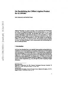
Cell 1 Cell 2 1× Bit-Wide Interconnect Tree
Cell 3
2× Word-Wide Interconnect Trees
. . . Cell n
Fig. 1. Example interconnect with two different interconnect types (bit-wide and word-wide). The word-wide interconnect is implemented as two parallel trees.
used to implement the actual application [6]. In this work an approach is presented, which provides the (semi-) automated generation of the pre-silicon circuit and can generate the configuration data for an actual application in the post-silicon phase. 2.1. Pre-Silicon Phase In the pre-silicon phase, the reconfigurable circuit is designed. As first step, its specification is derived from the set of (usually similar) actual applications, which will be implemented in the reconfigurable logic. During this design space exploration, the “needs of [the] applications [...] drive the construction of the fabric” [3, p. 1]. This approach requires the a-priori knowledge of all future applications and it is generally not possible to implement a different application with the resulting fabric. To enable yet unknown applications, we propose to include additional hardware and interconnect resources to the fabric. The specification includes information on the employed blocks (also called functional units) (e.g., adders, FSMs, ...), which can be reconfigurable themselves (e.g. an adder be reconfigured as a subtracter, reconfigurable FSM [7]). Additionally it includes the number of instances of each block as well as details on the connections among them. 2.2. Post-Silicon Phase After production in the post-silicon phase the actual application has to be implemented by configuring the silicon structure designed in the pre-silicon phase. So, on one hand, the postsilicon phase is limited by the results of the pre-silicon phase. On the other hand, the pre-silicon phase requires information on the actual implementations later used in the post-silicon phase to provide the required resources.
the according connection type by setting the proper configuration. 3. INTERCONNECT Most applications of coarse-grain reconfigurable logic are designed for computational tasks [4]. These use an array of homogeneous functional units connected with a highly regular interconnect (e.g. mesh structure), similar to FPGAs. In contrast, the presented approach assumes heterogeneous functional units (cell types), which also require a non-regular interconnect. 3.1. Requirements For the connection of the cells an interconnect topology with the following properties is required. 1. Allow random connections of the cells up to a certain degree. 2. Allow optimization of the interconnect for recurring pattern and similarities in the example netlists. 3. Can be characterized using a relatively simple and regular data structure. The existence of such a representation allows for easy manipulation and investigation of the interconnect topology. 4. Prohibits over-optimization to the example netlists that would prevent the interconnect to work with netlists that have similarities with, but are not identical to any example netlist. 5. Allow for easy oversizing of the interconnect resources to broaden the spectrum of implementable netlists. 6. Easy to implement with currently available logic synthesis tools.
2.3. Hardware Structure
3.2. Topology
For the presented algorithm, a few terms have to be defined. The circuit is built of multiple cells, which are instances of various cell types (previously called blocks, e.g. adder, FSM, lookup tables). Each has a number of input and output ports. Analogous to the separation of the control logic and the data-path in the FSM+D concept, each port of the cell types implements a connection type, e.g. bit-wide, word-wide or other categories. The connection types are defined based on compatible signaling (e.g. identical bit width) as well as semantics (e.g. clock enable vs. other control signal). All cells are connected using a reconfigurable interconnect. For every connection type a separate interconnect is implemented (see Fig. 1) which provides connections between all ports of its connection type. In the post-silicon phase, an actual application is implemented by connecting the cells as given by the netlist. This specifies nodes of certain cell types, which are mapped to the cells of the reconfigurable circuit. The ports of these nodes are connected with nets, which are routed via the interconnect of
Different interconnect topologies are evaluated in this section. The most powerful topology provides connections from every output to all inputs. The disadvantages are a large circuit overhead. On the other hand, a minimalistic interconnect with a small number of multiplexers to switch between alternative datapaths (compare [2]) does not allow to implement yet-unknown applications in the reconfigurable circuit. The topology proposed by [3, 8] uses alternating layers of functional units (FUs) and interconnecting MUXes. Although these MUXes only partially connect the FUs above and below the interconnect, the topology assumes a homogeneous pool of FUs. Mesh structures are an alternative to the layered topology, but also assume homogeneous FUs which can be configured to perform each of its basic functionalities. The interconnect itself requires a high number of switches which pose a high overhead in terms of silicon area and power. To reduce the large amount of hardware resources for the interconnect, FUs can be configured to route-through signals. On the other hand, this reduces
Switch 1
Cell 9
Switch 7
Cell 7
Cell 6
Cell 5
Switch 6
Cell 4
Cell 3
Switch 5
Cell 2
Cell 1
Switch 4
Switch 3
Cell 8
Switch 2
Fig. 2. Example interconnect with seven switches in three levels connecting nine cells of varying cell types the number of FUs available for processing tasks. To free up FUs in domain specific reconfigurable arrays, [9] augment the mesh network by additional links using inexact graph matching and the A∗ search algorithm. A mesh of heterogeneous FUs (adder, multiplier, constant, ...) for a domain-specific reconfigurable array is designed using a genetic algorithm [10]. It optimizes the placement of the FUs to reduce the wire length of the interconnect. The algorithm provides the physical structure (i.e., placement) of the reconfigurable circuit and extends mesh structures to heterogeneous FUs. Another topology for heterogeneous FUs are multistage interconnection networks (MINs) as Clos, Benes and Omega networks [11]. This topology poses two disadvantages: Firstly, the signal cannot be routed from an output to multiple inputs (multicast). This is tackled by the introduction of a copy-benes stage [12]. Secondly, the network is blocking, that means that certain combinations of signal routing cannot be implemented concurrently. By using two parallel MINs, this problem is reduced [12]. In SoCs, a bus topology is used to connect the CPU with the memory and all peripherals. For reconfigurable logic circuits with all cells working in parallel, this leads to high traffic and thus congestions [4]. The utilization of every cell is reduced and the total processing time protracted, which is not acceptable in the domain of low-power circuits. A tree based interconnect topology [13] allows to group the cells to provide short paths through lower levels of the tree for connections, which are used frequently by the different applications. On the other hand, connections to other nodes are still possible using higher hierarchical levels of the tree. This provides a large optimization potential to reduce circuit overhead but still results in a rich set of routing resources. 3.3. Tree Topology For the implementation of the reconfigurable modules, the tree topology was chosen to connect the individual cells due to its advantages and that it fulfils the above defined requirements. The interconnect is a tree (see Fig. 2) with the cells as leaf nodes and reconfigurable switches as inner nodes as well as the edges as connections (electrical nets).
The switches are unidirectional circuits which can be configured to connect any input port to any output port (see the detail in Fig. 2). The degree of a switch is the number of its children, (e.g., Switch 3 has a degree of two, Switch 6 has a degree of three). Each cell and each switch have a parent switch, except the top-most root switch. The height of the tree is the number of levels (e.g., Fig. 2 has a height of three). The routing length of a net is the number of switches it passes from its source cell to its destination cell. The total routing length is the sum for all nets of a given netlist. Each non-root switch in the tree has a number of connections to and from its parent switch. Only the number of these connections limits the capability of the interconnect to implement different netlists. Each switch can drive all outputs from any input, with one exception: A signal driven by one switch to another switch cannot be routed back to its originating switch. To improve the connectivity, for each connection type multiple parallel trees with identical topology can be implemented (as also implemented by [12], compare Fig. 3 and the two wordwide interconnect trees on the right side in Fig. 1). Each cell is assigned to a (generally different) leaf node in each tree. Therefore each net can be routed in any tree. As each cell might be assigned to a different leaf node in each tree, the routing length of a net can be small in one tree but high in the other trees. The tree interconnect provides numerous advantages in comparison with the alternatives in respect to the requirements established in Sec. 3.1. Ad 1) The netlists, which can be implemented by a given interconnect tree is only limited by the number of connections between the switches and their parent switches and the tree layout (number of levels and degree of switches). An interconnect with only one big root switch is equivalent to a full-MUX interconnect that can implement any netlist. This might be useful for connection types with only a small number of input or output ports. Ad 2) The interconnect can be optimized towards the similarities in the example netlists by choosing cell to tree leaf mappings in a way that minimizes the interconnect utilization of the example netlists. Ad 3) The whole interconnect can be described using only two simple data sets: Firstly the mapping of each cell to one leaf in each tree and secondly for each switch the number of
A Y
OUT[0]
IN[0]
FF[1]
ADD[0]
P
P
D Q
A B Y
MUL[3]
A Y
ADD[2] A B Y
MUL[0]
MUL[2]
FF[2]
D Q
A B Y
ADD[2]
A Y
MUL[4]
D Q
FF[0] A Y
P
IN[0] FF[0] D Q
A Y
MUL[1] MUL[3] A Y
A B Y
ADD[3] FF[2] D Q
A B Y
ADD[1] ADD[1] A B Y
P
OUT[0] FF[3] D Q
D Q
MUL[0] A Y
FF[1]
A Y
ADD[3] A B Y
MUL[2]
D Q
MUL[4] A Y
FF[3]
A B Y
ADD[0] MUL[1] A Y
Fig. 3. Exemplary interconnect for the digital filters shown in Fig. 5 using two parallel interconnect trees (top and bottom). The routed signal paths show the post-silicon configuration for the biquad-df1 filter. In the pre-silicon phase, the interconnect was optimized with the other three topologies. Note that the cells in the bottom half are the same as the cells in the top half, but in a different order, because they are mapped to different leaves in the second interconnect tree. connections to and from its parent switch. The first data set can be charaterized as a per-tree permutation and can be manipulated and optimized easily by exchanging the assignments of two cells in one tree. The second data set is a list of integers where greater value implies more flexibility in the post-silicon phase, but also more chip resources. Ad 4) As whole cells (instead of individual ports) are mapped to tree leaves, the optimization potential towards the individual datapaths is limited. There will always be nets that cannot be routed only by using the lowest layer of the interconnect. Thus smart grouping of cells can be used to optimize the interconnect to the requirements of the example netlists up to a certain degree. On the other hand, the interconnect will not be limited to the example netlists. Ad 5) Oversizing is done by increasing the number of connections between switches. Netlists which are similar but not part of the set of example netlists might have nets which result in a high routing length. With oversizing, extra routing resources help to improve these cases. Ad 6) The interconnect topology provides only unidirectional links. This allows for an implementation using MUXes built from standard cells, as generated by ASIC synthesis tools. For the interconnect in most up-to-date FPGAs, unidirectional links are also reconsidered [14]. An additional problem arises from potential combinational loops within the interconnect circuitry. This is eliminated by forbidding routing back a signal back to its originating switch. It is, however, still possible to create loops through combinational cells connected to the interconnect. This problem must be taken care of by breaking the loops when applying the synthesis constraints, e.g. using false paths and virtual clocks [15].
4. INTERCONNECT SYNTHESIS A tool called InterSynth was implemented, which automatically generates the interconnect for the reconfigurable module. It uses a set of example netlists (each representing an actual application, compare Sec. 2.1) with instances of cell types and connections among them. These are used to optimize the interconnect to provide cells and connectivity, able to implement any of these netlists. The output is a synthesizable Verilog file which instantiates the cells and describes the reconfigurable interconnect. In the pre-silicon phase, the algorithm first builds the interconnect topology with the given number of parallel trees, height of the trees and order of each level. The total number of leaves is given by the number of cells required by the example netlists. Then the cells are assigned to leaves in the interconnect trees (cell-to-leaf-mapping) and the required number of connections for each switch to and from its parent switch are determined so that the connections of all example netlists can be routed. In that course the algorithm also implements all example netlists. This means that for each netlist, each node is mapped to a cell (node-to-cell-mapping) and each net is routed via one of the interconnect trees. 4.1. Optimization Algorithm During the interconnect optimization, the cell-to-leaf-mappings are permuted, so that a smaller number of connections to and from the parent switches (and therefore hardware resources) are required to still implement all example netlists. This is preformed using an iterative algorithm, of which a single iteration is shown in Fig. 4. It operates on the state S , which contains all node-to-cell-mappings for all netlists and all cellto-leaf-mappings for all interconnect trees. The optimization is based on the Kernighan-Lin algorithm
S ← initial state function K ERN L IN O PTIMIZE(S, P , T ) j←1 S0 ← S while P contains compatible pairs do Sj ← Sj−1 (p1 , p2 ) ← best candidate pair from P Swap T mapping of p1 and p2 in Sj Remove p1 and p2 from P j ←j+1 end while S ← best candidate from S0 . . . Sj−1 end function if mode_align_netlists then repeat Sold ← S for all N = example netlist do P ← set of all nodes in N K ERN L IN O PTIMIZE(S, P , node_to_cell) end for until Sold = S end if for i = 1 → max. interconnect levels do if mode_swap_cell_mappings then for all I = interconnects with min. i levels do P ← set of all leaves in I K ERN L IN O PTIMIZE(S, P , cell_to_leaf) end for end if if mode_swap_node_mappings then for all N = example netlist do P ← set of all nodes in N K ERN L IN O PTIMIZE(S, P , node_to_cell) end for end if end for
Fig. 4. Intersynth Algroithm
[16], which is a heuristic procedure for solving partitioning problems by permuting the domain mappings of entities. In InterSynth it is used (in a slightly modified manner) to permute the node-to-cell- and cell-to-leaf-mappings in the state S . The function K ERN L IN O PTIMIZE in Fig. 4 implements the Kernighan-Lin algorithm. For the first iteration of the algorithm a start state S with random mappings is used. For all further iterations the result of the previous iteration is used as starting point. Experiments have shown that usually six iterations are enough to find a reasonable good solution. The algorithm is controlled using flags that enable or disable certain parts of the algorithm. Note that the K ERN L IN O P TIMIZE function is using different optimization goals in the different parts of the algorithm. So the term best candidate pair in
K ERN L IN O PTIMIZE is using a different definition of best depending on the calling block. The flag mode_align_netlists enables a block that “aligns” the netlists so similar subcircuits are mapped to the same set of cells. In this block the optimization goal for K ERN L IN O PTIMIZE is to minimize the number of unique pairs of connected cell ports over all netlists. The flag mode_swap_cell_mappings enables a block that permutes the cell-to-leaf-mappings for the individual interconnect trees and the flag mode_swap_node_mappings permutes the node-to-cellmappings. In both blocks the optimization goal is to minimize the sum of the total routing lengths for all netlists in the top i levels of the interconnect trees. Therefore the first iteration of the i-loop only tries to reduce the utilization of the root switch and further iterations of the i-loop refine this first solution with respect to the other switching levels in a top-down manner. For the pre-silicon procedure the algorithm is used with the flag mode_align_netlists enabled in the first iteration. Thus the actual algorithm is using aligned netlists as starting point. The flag mode_swap_cell_mappings is set for all iterations and mode_swap_node_mappings is only set for the second half of iterations. Thus the algorithm first tries to find a good solution without modifying the aligned netlists and after that uses this solution as starting point for an optimization run with all degrees of freedom. After this the number of required connections for each switch to and from its parent switch is calculated by using the maximum number of these connections used for each switch in the routing results generated by the algorithm. InterSynth also provides configuration options for the oversizing. In post-silicon runs the flag mode_align_netlists is never activated as there is only one netlist in post-silicon runs. The flag mode_swap_cell_mappings is also never set during the post-silicon procedure as the cell-to-leaf-mappings cannot be changed once the chip has been manufactured. The flag mode_swap_node_mappings is set in all iterations of the post-silicon procedure. As information about the available routing resources is available during the post-silicon procedure this information is used by the post-silicon routing algorithm. Thus the postsilicon routing algorithm does not optimize for shortest path but for least congestion. 4.2. Implementation Details The actual implementation of InterSynth is using performance optimizations. For example, instead of copying S to S0 , . . . , Sj−1 , a journal of the swaps is maintained that can be rolled back to the best solution. When the number of utilized nodes of a certain type varies between the netlists, additional “dummy nodes” are added by InterSynth to level the number of used nodes across all netlists. This is necessary as InterSynth can only permute the existing cell-to-leaf-mappings. So there must be mappings for all leafs in all trees in the initial state in order to make all possible mappings accessible to the optimization algorithm. The cell type descriptions used by InterSynth provide a flag to mark a cell input as possible feedback input. An input which does not have this flag set cannot be connected
directly to an output from the same cell. For most cell types such connections would never be part of a valid netlist. The Verilog HDL code generated by InterSynth can be used as-is in the final ASIC design as InterSynth can be configured to not only include the cell instantiations and interconnect logic but also additional support code in the HDL output, such as connections of cell ports to ports of the generated module (for input and output purposes or distributing global signals such as clock and reset). It is also possible to embed configuration data for reconfigurable cells (ALUs, etc.) within the InterSynth config bitstream. Inputs and outputs to the whole reconfigurable modules are handled as special cell types and therefore are not explicitly drawn in Fig. 1 and 2. The automatically generated interconnect shown in Fig. 3 only has one input and one output labeled IN[0] and OUT[0].
5. DESIGN FLOW INTEGRATION The integration of InterSynth in the design flow starts with the specification of the application class of a reconfigurable module and multiple example applications (pre-silicon phase). From these applications, the required cell types are derived and defined using appropriate connection types. These are used in the netlists created for all example applications. In the manual design flow described in [5], these cell types are instantiated in a hierarchical and structured design. Three connection types (bit, byte and word) were used to connect the peripherals (ADC, serial bus masters, ...) with the control logic (using a TR-FSM [7]), the byte memory and the arithmetic unit. The interconnect is also implemented hierarchically using large multiplexers and switch boxes. For the automated design flow, the whole reconfigurable module is implemented as a pool of cells. The interconnect is constructed and optimized by InterSynth to fulfil the requirements of the examples application. The user provides the definition of the connection types and the interfaces of all cell types. The example netlists instantiate these cells and specify the nets connecting them. Additionally, the designer can provide various tuning parameters, such as the number of parallel trees and oversizing rules. The output of InterSynth is the Verilog HDL source code, which instantiates the optimized set of cells and describes the reconfigurable interconnect. This file can be used directly for the ASIC synthesis. It also creates a description of the created circuit to be used in the post-silicon phase. Additionally, debug output in various formats like the TikZ-image in Fig. 3 can be generated. In the post-silicon phase, the circuit description created by the pre-silicon phase is used together with the netlist of the actual application. InterSynth creates the configuration bitstream for the reconfigurable module to implement this application. Again, optional debug output is available.
6. EVALUATION Two different application classes were used to evaluate InterSynth: digital filters (see Sec. 6.1) and logic functions (see Sec. 6.2). For both an identical interconnect configuration was used, which has two parallel trees of height three (although with different connection types). The switches in the bottom two layers have a degree of four and the top level (root) switch connects all switches of the second layer. In order to create more flexible interconnects, an oversizing rule for one additional connection to each switch to and from its parent switch was used. 6.1. Filter Networks Two instances of the four different digital filter topologies as shown in Fig. 5 were concatenated in all 16 possible combinations to build netlists of higher-order filters. The cell types employed are (word-wide) adders, multipliers and flip-flops. Test 1) From the pool of 16 netlists a random sample of n was selected and used for the pre-silicon phase to optimize the interconnect. Then the post-silicon phase was attempted with each of the 16 netlists. This test was performed 1000 times each for n ∈ {1, . . . , 6}. The number of attempts, in which the netlist could not be routed within the interconnect generated by the pre-silicon phase are shown in the center part (green background) of Tab. 1 for each n (columns) and each post-silicon netlist (rows). It shows, that increasing the number of example netlists n in the pre-silicon phase results in less failed attempts in the post-silicon phase. The average resource usage of the generated interconnect is expressed with two figures: the number of bits of the configuration data and the number of 2-to-1 MUXes (MUX2) required to build the interconnect. Both numbers are normalized to the total number of cell ports. The bottom part (yellow background) of Tab. 1 gives their mean and the standard deviation for n ∈ {1, . . . , 6}. For the case of n = 1 pre-silicon netlist, the average number of MUX2 is shown in the right part of the table separated for every pre-silicon netlist type (blue background).
biquad-df1
biquad-df2
fir4-df1
fir4-df2
Fig. 5. Filter topologies used as test netlists. Circles represent adders, squares represent delays and triangles represent configurable constant factor multipliers.
Table 1. Filter Network Post-Silicon Errors vs. Number of Pre-Silicon Netlists 6
1 Pre-Si. Netl. mux2 dev
biquad-df1.biquad-df1 biquad-df1.biquad-df2 biquad-df1.fir4-df1 biquad-df1.fir4-df2
138 40 130 27
5 2 6 1
1 0 0 0
0 0 0 0
0 0 0 0
0 0 0 0
6.6 6.6 6.7 6.6
0.26 0.30 0.32 0.27
biquad-df2.biquad-df1 biquad-df2.biquad-df2 biquad-df2.fir4-df1 biquad-df2.fir4-df2
34 22 46 40
0 2 1 2
0 0 0 0
0 0 0 0
0 0 0 0
0 0 0 0
6.5 6.6 6.6 6.6
0.30 0.29 0.31 0.25
fir4-df1.biquad-df1 fir4-df1.biquad-df2 fir4-df1.fir4-df1 fir4-df1.fir4-df2
144 38 160 60
3 2 5 3
1 0 0 0
0 0 0 0
0 0 0 0
0 0 0 0
6.6 6.6 6.7 6.7
0.33 0.28 0.25 0.26
fir4-df2.biquad-df1 fir4-df2.biquad-df2 fir4-df2.fir4-df1 fir4-df2.fir4-df2
69 36 71 361
3 2 0 56
0 0 0 11
0 0 0 5
0 0 0 3
0 0 0 0
6.5 6.7 6.7 6.7
0.28 0.28 0.28 0.25
avg. bits / port avg. mux2 / port
4.7 6.6
5.3 8.2
5.8 9.6
6.3 10.9
6.7 12.0
6.9 12.8
dev. bits / port dev. mux2 / port
0.13 0.29
0.27 0.72
0.30 0.82
0.30 0.79
0.28 0.76
0.27 0.79
The test also shows that the topology fir4-df2.fir4-df2 can not be implemented with a small fraction of the generated interconnects while the other topologies can be implemented in all tests with n ≥ 4 example netlists. This can be explained by the differences in the fir4-df2 topology compared to the other three topologies in Fig. 5: All multipliers in fir4-df2 are driven directly from the input (which therefore has a fanout of five) and all delay outputs are connected to adder inputs while in the other topologies delay outputs are connected to delay or multiplier inputs. It is worth mentioning that fir4-df2.fir4-df2 does not require more routing resources than the other topologies (see right part of Tab. 1). It only requires a different interconnect because it is composed of different patterns. Thus an interconnect that can implement fir4-df2.fir4-df2 as well as the other 15 topologies needs more resources than one that can only implement the 15 others. Test 2) The resource usage of the pre-silicon results where compared to the resource usage of an interconnect with a random, i.e, unoptimized cell-to-leaf-mappings (mode_swap_cell_mappings disabled in all iterations of the algorithm). The difference in the resources needed for these two cases is an indicator of the optimization potential utilized by InterSynth to optimize the interconnect for the application domain described by the example netlists. When n = 4 pre-silicon netlists are used and no additional routing resources are added, an average number of 3.0 (stddev 1.1) word-wide MUX2 per cell port are required to implement the filter example. When the InterSynth cell to leaf mapping is replaced with a random mapping and InterSynth is only used for the node-to-cell-mappings, this number increases to 7.2 (stddev 0.6). This shows that InterSynth can drastically optimize interconnects for scenarios like this one with a relatively large number of cell types compared to the number of cells. Test 3) The number of parallel interconnect trees was var-
2
Degree of Interconnect Trees 3 4 5 6
1 2 3 4
10.74 8.51 8.48 9.57
8.39 7.86 8.57 10.21
8.42 8.27 9.75 12.23
7.21 8.31 10.39 13.22
8.34 9.14 11.80 15.22
MUX2
Number of Pre-Silicon Netlists 2 3 4 5
1 2 3 4
116 46 0 0
82 34 0 0
81 5 0 0
43 6 0 0
32 2 0 0
Post. Err.
1
Number of Trees
Topology
Table 2. Number of Trees and Degree of Switches vs. Interconnect Resource Usage and Post-Silicon Errors
ied from one to five and the degree of the switches was varied from two (binary tree) to six. For each of these interconnect configurations, two random pre-silicon netlists where used for optimization. The average resource utilization (number of MUX2) for each configuration is given in the top part (green background) of Tab. 2. Each optimized interconnect was used for 1000 post-silicon netlists. The number of errors (i.e., the post-silicon netlist could not be routed within the interconnect) is shown in the bottom part (yellow background) of Tab. 2. For a single interconnect tree, even with a high degree of the switches a large number of post-silicon errors are present. Two parallel trees and a degree of four and above result in an acceptable number of post-silicon errors. Therefore two parallel trees with switches of degree four are a trade-off with resource utilization. More parallel trees result in a large increase of resource utilization and also might result in a wiring congestion on chip in larger scenarios. 6.2. Logic Networks Random logic functions with six input and one output where generated and ABC [17] was used to convert these logic functions to netlists of inverters, two-input AND gates and two-input XOR gates. Of course such a problem would be better solved using lookup tables rather than configurable interconnects and basic logic gates, but this is a simple method for generating a virtually unlimited pool of “similar” large netlists. For this test InterSynth was configured with oversizing rules to add 10 % plus 5 cells of each kind to compensate for the variation in the cell usage in the generated netlists. Test 1) For the pre-silicon phase, four random example netlists were used to optimize the interconnect. The results from this pre-silicon phase were then tested using 1000 other random netlists (limited by the number of available cells) for the post-silicon phase. This was performed 50 times. The post-silicon run failed in only 0.05 % of these 50000 tests. Test 2) An average number of 16.8 (stddev 0.8) MUX2 per cell port are required to implement this testcase (with four presilicon netlists) regardless of whether the cell-to-leaf-mapping was optimized or not (i.e, mode_swap_cell_mappings was enable or disabled). This shows that while it is possible to use
InterSynth for large homogeneous networks like this test case, it doesn’t have an advantage over distributing the cells regularly.
[5] J. Glaser, K. Gravogl, J. Haase, and C. Grimm, “A Reconfigurable Architecture for Ultra-Low Power Wireless Sensors,” The Mediterranean Journal of Electronics and Communications (MEDJEC), vol. 7, no. 3, pp. 255–266, 2011.
7. CONCLUSION
[6] J. Glaser, J. Haase, and C. Grimm, “Designing a Reconfigurable Architecture for Ultra-Low Power Wireless Sensors,” in Proceedings of the Seventh IEEE, IET International Symposium on Communication Systems, Networks and Digital Signal Processing (CSNDSP), Z. Ghassemlooy and W. P. Ng, Eds., Northumbria University, Newcastle upon Tyne, United Kingdom, 21.-23. July 2010, pp. 343–347.
A tool is presented that automatically optimizes a heterogeneous coarse-grain reconfigurable logic architecture. In the presilicon phase, the application class for the reconfigurable module is defined and specified by several example applications. These are used by the presented algorithm to optimize a tree structured interconnect and the selection of the building blocks which are able to implement all example applications. Spending additional hardware resources even allows to implement yet-unknown applications with the resulting silicon. The tool is used in the post-silicon phase to map the netlists of the actual applications to the logic circuit. The evaluation of the algorithm was performed using digital filter topologies. With only two example netlists and slight oversizing in the pre-silicon phase, nearly all other example netlists could be realized in the post-silicon phase. Additionally, a large optimization potential to keep the hardware resources limited was demonstrated. Future development will integrate the generalization of building blocks, e.g. an ALU as a replacement for different simple arithmetic operations [2]. The routing algorithm for pre- and post-silicon phase will be improved, for example to support the routing of a single net in multiple trees. As depicted in the bottom part (yellow background) of Tab. 1, the hardware resources (MUX2) of the interconnect increase when more presilicon netlists are used, even when all example netlists can be routed. A consolidating step after the pre-silicon procedure will reduce the hardware resources. InterSynth is a generic tool for creating interconnects using the procedure described in this paper. It is implemented in C++ and released as Open Source project at http://www.clifford. at/intersynth/. The scripts used to run the experiments in Sec. 6 are included. 8. REFERENCES [1] J. Glaser, J. Haase, M. Damm, and C. Grimm, “Investigating Power-Reduction for a Reconfigurable Sensor Interface,” in Proceedings of Austrochip 2009, Graz, Austria, 7. Oct. 2009. [2] J. Ou, F. Muhammad, J. Haase, and C. Grimm, “A Technique for the Identification of Reconfigurable Resources of Flexible Communication Systems,” in NASA/ESA Conference on Adaptive Hardware and Systems (AHS), June 2011, pp. 256–263. [3] G. Mehta, J. Stander, J. Lucas, R. R. Hoare, B. Hunsaker, and A. K. Jones, “A Low-Energy Reconfigurable Fabric for the SuperCISC Architecture,” Journal of Low Power Electronics, vol. 2, no. 2, pp. 148–164, Aug. 2006. [4] Z. ul Abdin and B. Svensson, “Evolution in architectures and programming methodologies of coarse-grained reconfigurable computing,” Microprocessors and Microsystems, vol. 33, no. 3, pp. 161– 178, 2009.
[7] J. Glaser, M. Damm, J. Haase, and C. Grimm, “TR-FSM: Transition-based Reconfigurable Finite State Machine,” ACM Transactions on Reconfigurable Technology and Systems (TRETS), vol. 4, no. 3, pp. 23:1–23:14, Aug. 2011. [8] G. Mehta, J. Slander, M. Baz, B. Hunsaker, and A. Jones, “Interconnect customization for a coarse-grained reconfigurable fabric,” in Parallel and Distributed Processing Symposium, 2007. IPDPS 2007. IEEE International, Mar. 2007, pp. 1–8. [9] J. Yoon, J. Lee, J. Jung, S. Park, Y. Kim, Y. Paek, and D. Cho, “I2 CRF: Incremental Interconnect Customization for Embedded Reconfigurable Fabrics,” in Design, Automation Test in Europe Conference Exhibition (DATE), Mar. 2011, pp. 1–6. [10] W. Fung, T. Arslan, and S. Khawam, “Genetic algorithm based engine for domain-specific reconfigurable arrays,” in First NASA/ESA Conference on Adaptive Hardware and Systems, AHS 2006, June 2006, pp. 200–206. [11] R. Ferreira, M. Laure, A. Beck, T. Lo, M. Rutzig, and L. Carro, “A low cost and adaptable routing network for reconfigurable systems,” in Parallel Distributed Processing, 2009. IPDPS 2009. IEEE International Symposium on, may 2009, pp. 1–8. [12] R. Ferreira, J. Vendramini, L. Mucida, M. Pereira, and L. Carro, “An FPGA-based heterogeneous coarse-grained dynamically reconfigurable architecture,” in Proceedings of the 14th International Conference on Compilers, Architectures and Synthesis for Embedded Systems (CASES), Oct. 2011, pp. 195–204. [13] Z. Marrakchi, H. Mrabet, U. Farooq, and H. Mehrez, “FPGA interconnect topologies exploration,” International Journal of Reconfigurable Computing, vol. 2009, pp. 1–13, 2009. [14] G. Lemieux, E. Lee, M. Tom, and A. Yu, “Directional and single-driver wires in FPGA interconnect,” pp. 41–48, IEEE. [15] H. Bhatnagar, Advanced ASIC chip synthesis using Synopsys Design Compiler, Physical Compiler, and PrimeTime, Kluwer Academic Publishers, Boston, 2002. [16] B. W. Kernighan and S. Lin, “An efficient heuristic procedure for partitioning graphs,” Bell System Technical Journal, vol. 49, no. 1, 1970. [17] Berkeley Logic Synthesis and Verification Group, “ABC: A System for Sequential Synthesis and Verification,” HG 120213 http://www.eecs.berkeley.edu/~alanmi/abc/.