yield and high clock frequency even at scaled supply voltage. The idea is based on ... Low Power, Process Tolerant, Hybrid Adder, Adaptive Clock. Stretching ...
Exploring High-Speed Low-Power Hybrid Arithmetic Units at Scaled Supply and Adaptive Clock-Stretching Swaroop Ghosh and Kaushik Roy School of Electrical and Computer Engineering, Purdue University, West Lafayette, IN 47907 < ghosh3, kaushik>@ecn.purdue.edu
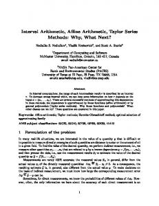
Mux
Adder Core
Logical o/p
Mux control Sign control
Fig. 1 Basic ALU organization Pre-decoder
●●●
Arithmetic and Logic Units (ALU) are the core of microprocessors where all computations are being performed. Demand for performance at low power consumption in today’s general purpose processors has put severe limitations on ALU design. ALUs are also one of the most power hungry sections in the processor and are often the possible location of hot-spots. The presence of multiple ALUs in superscalar pipelines further deteriorates the power and thermal issues [1]. Technology scaling has resulted in faster devices but at the same time the die-to-die delay variations has increased due to different lithographic subtleties. Therefore, low power ALU design while maintaining high yield under tighter delay constraint turns out to be a multidimensional problem. Typically, the core of the ALU consists of an adder which takes operands from register file, data cache or ALU writeback bus. The input multiplexers select the proper operands among these and provide the ALU inputs. The adder output is multiplexed with the logical output through an output multiplexer. The basic structure of the ALU is shown in Fig. 1. Since multiplication is a less frequent
Mux
I. INTRODUCTION
External operands
Mux
Low Power, Process Tolerant, Hybrid Adder, Adaptive Clock Stretching, Supply Voltage Scaling
Shift control
Mux
Keywords
Mux control External operands
Mux
Abstract— Meeting power and performance requirement is a challenging task in high speed ALUs. Supply voltage scaling is promising because it reduces both switching and active power but it also degrades robustness. Recently, researchers have proposed novel design technique for linear time complexity adders that maintain high yield and high clock frequency even at scaled supply voltage. The idea is based on the fact that the critical paths of arithmetic units are exercised rarely. The technique (a) predicts the set of critical paths, (b) reduces the supply voltage to operate non-critical paths at rated frequency, and; (c) avoids possible delay failures in the critical paths by dynamically stretching the clock period (to say, two-cycles assuming all standard operations are single-cycle), when they are activated. This allows circuits to operate at scaled supply with minimal performance degradation. The off-critical paths operate in single clock cycle while critical paths are operated in stretched clock period. Different classes of adders may benefit differently using such technique. For example, ripple carry adders can reap the benefits more effectively than say, tree adders (balanced paths). However, logic modification may ease the application of supply voltage scaling. In this paper, we explore various arithmetic units for possible use in high speed, high yield ALU design at scaled supply voltage with variable latency operation. We demonstrate that careful logic optimization of the existing arithmetic units indeed make them further suitable for supply voltage scaling with tolerable area overhead. Simulation results on different adder and multiplier topologies in BPTM 70nm technology show 18-60% extra improvement in power with only 2-8% increase in die-area at iso-yield. We also extend our studies to design low power and high yield multipliers. These optimized low power datapath units can be used to construct low power and robust ALU that can operate at high clock frequency with minimal performance degradation due to occasional clock stretching.
FA 31
C17 ●●●
FA 17
FA 16
FA 15
FA 14
FA 13
S17
S16
S15
S14
S13
●●● C12
FA 0
Cin=0
Cout S31
S0
Prediction of critical path activation
(a) Instruction 1
Instruction 2
Instruction 3
CLK cycle 1
cycle 2
cycle 3
cycle 4
computation Adaptive CLK Tc
2Tc
Tc
(b) Fig. 2 (a) Basic structure of variable latency adder, and; (b) adaptive clock stretching operation in variable latency adder (Tc is the clock period)
operation than addition/subtraction/shift operation, the multipliers are usually isolated from the ALU. This also ensures the high speed operations of the more frequent instructions. However, for signal processing applications (e.g., filters, DCT), the multipliers can be an integral part of the ALU. Supply voltage scaling is very effective in reducing the power dissipation due to quadratic dependency of switching power on supply voltage and linear dependence of sub-threshold leakage. Variable supply voltage and adaptive body biasing technique has been proposed in [2] to jointly optimize the switching and leakage power of a multiply-accumulate unit. In this technique, a critical path replica is used to predict the performance while body biasing is used to tune the threshold voltage of the actual circuit. Adaptive supply voltage is also used to match circuit speed with the clock frequency and to reduce power consumption. In [3] [4], the authors reduce the power consumption by observing the fact that the critical paths of arithmetic units are exercised rarely. Therefore, the supply voltage can be scaled down (while maintaining the clock frequency) to utilize the timing slack available between the critical paths and the longest off-critical paths. The off-critical paths are evaluated in rated frequency while the infrequent critical
A5
A4
A3
A2
A2
A5
A4
A3
A2
A2
31 30 29 28 27 26
M9
M10
M8
M6
M7
M5
M2
M3
M4
M1
C i1=1
Cout
C i0 =0
Co0
Co1
25 24 23 22 21 20 19 18 17 16
15 14 13 12 11 10
9
8
7
6
5
4
3
2
31:30
15:14 14:13 13:12 12:11 11:10 10:9
9:8
8:7
7:6
6:5
5:4
4:3
3:2
2:1
31:28
15:12 14:11 13:10 12:9 11:8 10:7
9:6
8:5
7:4
6:3
5:2
4:1
3:0
2:0
31:24
15:8 14:7 13:6 12:5 11:4 10:3
9:2
8:1
7:0
6:0
5:0
4:0
1
0
1:0
31:16
Cin= 0 A5
A4
Stage 10
A3
A2
A2
A5
A4
A3
A2
A2
Stage 1
Stage 6
15:0 14:0 13:0 12:0 11:0 10:0 9:0 8:0 7:0 6:0 5:0 4:0 3:0 2:0 1:0 0:0
31:0
(a) 31 30 29 28 27 26
25 24 23 22 21 20 19 18 17 16
(b)
15 14 13 12 11 10
9
8
7
6
5
4
3
2
1
0 31 30 29 28 27 26
31:30
15:14
13:12
11:10
9:8
7:6
5:4
3:2
31:28
15:12
13:10
11:8
9:6
7:4
5:2
3:0
31:30
31:24
15:8
13:6
11:4
9:2
7:0
25 24 23 22 21 20 19 18 17 16 15 14 13 12 11 10
9
8
7
6
5
4
3
2
1
0
1:0 15:14
13:12
11:10
23:22
31:28
23:20
31:24
23:16
7:6
19:18 19:16
17:16
15:14 15:12 15:8
13:12
11:10 11:8
9:8
7:6 7:4
5:4
3:2
1:0
3:0
7:0
5:0 31:16
31:16
31:0
15:014:013:012:011:010:0 9:0 8:0 7:0 6:0 5:0 4:0 3:0 2:0 1:0 0:0
31:0
15:014:013:012:011:010:0 9:0 8:0 7:0 6:0 5:0 4:0 3:0 2:0 1:0 0:0
(d) (c) Fig. 3 Critical and off-critical paths of various 32-bit adders (a) C2SA, (b) Kogge-Stone, (c) Han-Carlson, and; (d) Brent-Kung (the shaded bits have been pre-decoded for prediction of critical path activation). The pre-decoder is not shown in the figure.
paths are evaluated in two-clock cycles. This allows aggressive scaling of supply voltage with minimal throughput degradation. A pre-decoder is used to predict the activation of critical paths based on input pattern. In [3], the application of this methodology is shown for ripple carry adder. A new adder called “cascaded carry select adder (C2SA)” is proposed in [4] which improves the existing carry select adder (CSA) to make it amenable to supply voltage scaling and variable latency operation. Various adder families [5][6][7][8] have been proposed in the past to tradeoff speed, power and area for possible use in ALU. So far, ripple carry adder (RCA) turned out to be the most area and energy efficient but with worst critical path delay. CSA is faster than RCA however, it has larger area due to logic duplication. Kogge-Stone (KS) [6] on the other hand, is among the fastest adders but consumes large area and power. Therefore, a family of sparse tree adders have been proposed (e.g., Brent-Kung, HanCarlson, Sklansky etc) to reduce area at the cost of slight increase in delay. In Brent-Kung (BK) [7], the forward tree computes the longest carry fast and the intermediate carries are computed by a backward tree. Han-Carlson (HC) [8] computes the even carries first and generates the odd carries using a backward tree. In practice, sparse tree adders (e.g., HC) are preferred over faster KS for designing ALU’s in order to reduce wiring and area overhead. In [5], the various tree adders have been compared in energy-delay space. However, the adders have not been explored in terms of supply voltage scaling and variable latency operation for low power and high yield ALU design. In this paper, we explore various topologies of adders (e.g., RCA, C2SA, KS, BK, HC) in terms of their amenability to the above mentioned supply voltage scaling and variable latency operation for critical paths. We compare the power, area, speed and yield of these adders at scaled supply to find the best candidate suitable for high speed and low power dissipation. We further propose careful optimization to design hybrid adders that would
allow further scaling of supply voltage with small area penalty. We also extend this study to the design of low power multiplier. In summary, we make following contributions in this paper, • Comparison of adders in terms of power, area, speed and yield at scaled supply with variable latency operation for high speed and low power ALU design. • Propose hybrid adder design methodology that optimizes the off-critical paths of the adders to allow further scaling of supply voltage with improved yield. • Application and analysis of similar technique for the design of low power multiplier at scaled supply. The rest of the paper is organized as follows. In Section II, we briefly discuss supply voltage scaling and variable latency operation for low power ALU design. We also explore different adder topologies for power, speed and yield. We propose hybrid adder design methodology to allow further scaling of supply voltage in Section III. A low power multiplier is presented in Section IV. In this section, we use the hybrid adder design in the vector merging stage of carry save multiplier (CSM) architecture. Finally, conclusions are drawn in Section V.
II. LOW POWER ADDERS AT SCALED SUPPLY In this section, first we briefly discuss the concept of variable latency adders at scaled supply. Next, we analyze different types of adders namely, RCA, C2SA, KS, BK and HC in terms of their applicability to supply scaling, speed, area and tolerance to process variation. A. Variable Latency Adders Variable latency adders are based on the fact that the critical paths are activated occasionally. Therefore supply voltage can be scaled down while maintaining the rated frequency. The offcritical paths are evaluated in 1-cycle (at rated frequency) while the clock period is stretched to 2-cycles when the critical paths are
0.03 0.02 0.01 C2SA
KS HC BK Adder topology
RCA
400 200 0 C2SA
KS HC BK Adder topology
RCA
PDP analysis of conventional adders 8 Nominal VDD Low VDD 6
Power analysis of conventional adders 80 60
7
PDP(x10 )
0.04
Power analysis of conventional adders 800 Nominal VDD Low VDD 600
Power saving(%)
Power( µ W)
σ /µ
Process variation in conventional adders 0.06 Critical Off-critical 0.05
40
2
20 0 C2SA
4
KS
HC BK Adder topology
RCA
0 C2SA
KS HC BK Adder topology
RCA
(c) (d) (a) (b) Fig. 4 Comparison of variable latency adders in terms of: (a) process variation, (b) power dissipation, (c) % power saving, and; (d) power-delay product
activated. This allows us to utilize the timing slack between critical and off-critical paths for supply voltage scaling. A pre-decoder is required to predict the activation of critical paths based on the input pattern. The basic structure of a 32-bit variable latency ripple carry adder is shown in Fig. 2(a). Since decoder consumes area, only few intermediate bits are decoded to predict critical path activation. In Fig. 2, bit-13 through bit-17 is decoded to predict whether the current input pattern can propagate the input carry (C12) through bit-17. The decoding circuit is nothing but a set of XOR gates that determines whether p13.p14…p17 = 1 or not (where p’s are propagate [10]). For this choice of decoding, path C1 through Cout is the longest critical path whereas paths C1 through S17 and C13 through S31 are the longest off-critical paths. The adder supply is scaled down while keeping the frequency same such that the longest off-critical paths can be computed without any delay failure. For other longer paths, the decoder output is automatically asserted and a clock stretching operation is performed to avoid timing failure. Note that in this example, any path longer than 17 full adder delay is considered critical, and evaluated in stretched clock to avoid delay failure. For the sake of convenience, we use the term off-critical paths to refer to longest off-critical paths. The adaptive clock stretching operation in variable latency adders is further elucidated in Fig. 2(b) with the help of timing diagram for three pipelined instructions. Let us assume that out of these three instructions, the second instruction activates the critical path. Therefore adaptive clock stretching should be performed during the execution of second instruction for correct functionality of the pipeline. The regular clock and adaptive clock is shown in Fig. 2(b) for the sake of clarity. Note that, the second instruction is fired at cycle-2 but evaluated in cycle-4 by using the adaptive clock. This is achieved by gating the clock edge in cycle-3 based on the output of critical path prediction logic. Although better critical path prediction can made and performance penalty can be reduced by decoding more bits, the power/area overhead increases with decoder size. It has been shown in [9] that ~6-10 bit decoding is optimal. In the rest of the paper, we have decoded 7 bits from the middle of the adder for analysis and simulation purposes. B. Analysis of Different Adder Topologies Fig. 3 shows the 32-bit C2SA, KS, BK and HC adders with their critical path and two off-critical paths that determine the supply voltage scaling. The critical path is shown with bold line whereas the off-critical paths are shown with dashed lines. In C2SA [4], the cascading is done by dividing the 32-bits into chunks of {2, 2, 3, 4, 5, 2, 2, 3, 4, 5}. The partial sum is computed in parallel for Cin =0 as well as Cin =1 using RCA. Next, the multiplexers select the appropriate sum based on the actual carry. In the tree adders (Fig. 3), black squares denote the computation of
propagate and generate (pg) whereas grey squares denote computation of generate (g) only. The buffers are denoted by empty triangles. Intuitively, RCA is expected to allow better supply voltage scaling because of large timing slack present between critical and off-critical paths. However, the speed of the adder itself is slow. Tree adders, for example KS, are fast because it tries to compute all paths in parallel. But in the process, it also reduces the timing slack between critical and off-critical paths. Further the dense routing wires increase area as well as delay. Sparse tree adders like BK and HC, trade-off the area with speed and also reduce the wiring overhead. The delay of critical path also determines the adder’s tolerance to process variation. Longer paths may experience less variations compared to shorter paths due to cancellation effect (i.e, the average current drawn by the logic gates in longer path remains same under intra-die process variation). For analysis of adders, we experimented with 32-bit and 64-bit adders synthesized using Synopsis design compiler [11]. The simulation is done using Hspice with BPTM 70nm [12] devices. The process variation is modeled as lumped Vth variations due to inter- and intra-die process fluctuations. The (mean, sigma) of inter-die and intra-die variation is taken to be (0, 40mV) and (0, 20mV), respectively. The Vth of the transistor is given by the summation of nominal Vth and change in Vth due to inter- and intra-die process variations. The operating frequency of the adders at nominal supply (1V) is chosen such that the critical path meets 95% yield target. Supply voltage scaling is performed so that critical paths meet 100% yield while the off-critical paths meet 95% yield with respect to their delay targets. As discussed earlier, adaptive clock stretching is used with prediction logic to avoid delay failures at reduced supply voltage. C. Impact of Process Variation We have plotted the σ/µ for different 32-bit adders in Fig. 4(a) to observe the impact of process variation. Following points can be noted from this plot: (a) the off-critical paths are more susceptible to process variation. This is intuitive because the off-critical paths are shorter and hence the impact of intra-die process variation may not cancel out and, (b) the faster adders are more prone to variations compared to slower adders. This is true because slow adders have longer critical paths and the change in current drawn by the gates due to process variation averages out; resulting in small σ/µ. Therefore, for tolerance to process variation, RCA and BK are the best choice. D. Comparison in Terms of Power Dissipation For power estimation, we apply a set of 1000 random test patterns to the adders and compute the average power using Nanosim [13]. Fig. 4(b) shows the power dissipation at nominal
P re -d e co d e r
● ● ●
● ● ●
FA 31 ● ●C17 ●
●●● C12
KS Adder
31 30 29 28 27 26
31:30
FA 0
15:14
13:12
25 24 23 22 21 20 19 18 17 16 15 14 13 12 11 10
11:10
23:22
31:28
23:20
31:24
23:16
7:6
17:16
19:18
15:14
19:16
6
7:6
5
5:4
7:4
15:8
4
3
2
3:2
1
0
1:0
3:0
7:0
S12
● ● ●
critical path activation
S0
15:014:013:0 12:011:010:0 9:0 8:0 7:0 6:0 5:0 4:0 3:0 2:0 1:0 0:0
(b) Delay variation in C2SA adder (Nominal Voltage)
KS Adder A2
A5
A4
A3
A2
A2 Co0
M9
M10
M6
M7
M8
M5
M2
M3
M4
M1
Cin= 0 A5
A4
A3
A2
A2
A5
A4
A3
KS Adder Stage 6
A2
Off-critical (Conv) Critical (Conv) Off-critical (Hyb) Critical (Hyb)
0.12
0.08
0.1
0.06
0.04
0.04
0.02
A2
0.05
0 0
0.5
1 Delay (ns)
1.5
0 0
2
1
600 500
Conv (32-Bit) Hyb (32-Bit) Conv (64-Bit) Hyb (64-Bit)
400
σ /µ
Conventional Hybrid
300
0.04
200
0.02
30
100 0 C2SA
BK Adder topology
RCA
0 C2SA
BK Adder topology
0 0
4
1
2
3 4 Delay (ns)
5
6
7
Area Overhead of hybrid adders
70
700
BK Adder topology
RCA
Extra Power Saving (%)
50
3
Power comparison (at low voltage)
Power comparison (at low voltage)
P ow er ( µ W )
Process variation in hybrid adders
2 Delay (ns)
(d)
(c) 60
0.1
0.02
Stage 1
Process variation in hybrid adders 0.08 Conventional Hybrid 0.06
0.15
0.08
0.06
Co1
Stage 10
0.1
Delay variation in BK adder (Low Voltage) Off-critical (Conv) Critical (Conv) Off-critical (Hyb) Critical (Hyb)
0.2
0.14
# o f o c c u re n c e s
A2
C i0 =0
A3
Delay variation in BK adder (Nominal Voltage)
Off-critical (Conv) Critical (Conv) Off-critical (Hyb) Critical (Hyb)
# o f o cc u ren ces
A4
C i1 =1
A5
0.12
# o f o ccu ren ces
S19
31:0
σ (ps)
7
31:16
(a)
20 C2SA
9:8
11:8
32b 64b
60 50 40 30 20
10 % A rea Overhead
S31
40
11:10
8
Cin=0 Prediction of
Cout
Cout
13:12
15:12
9
8 6 4 2
64-Bit Adders 32-Bit Adders
10 0 C2SA
BK Adder topology
RCA
0 C2SA
BK Adder topology
RCA
RCA
(f) (e) Fig. 5 Hybrid adders (a) RCA, (b) Brent-Kung, (c) C2SA, (d) delay distribution of hybrid adders under process variation, (e) comparison of hybrid adders and conventional adders in terms of process variation, (f) comparison in terms of power saving for 32-bit and 64-bit adders and corresponding area overhead
supply voltage as well as at reduced supply voltage. At reduced supply, we maintain 95% yield with respect to the off-critical path delay and 100% yield with respect to the critical path delay. The adder is operated with variable latency using adaptive clock stretching to avoid delay failures at reduced supply. For the sake of comparison, we also plot % saving in power for these adders (Fig. 4(c)). The important points from this figure are (a) C2SA adder consumes highest power due to large area and switching capacitance, RCA on the other hand consumes smallest power, (b) the % power saving also increases as we move towards the slower adders. Fig. 4(d) shows the power-delay product (PDP) of the adders. The faster adders consume large power resulting to increased PDP whereas slower adders consume less power leading to small PDP. The plot suggests that HC or BK can be the best choice for low power with variable latency operations. From the above discussions, it is apparent that BK is reasonable both in terms of robustness as well as PDP. The RCA is at one extreme with good robustness and reasonable PDP however, it is too slow to be practical for high performance ALUs. C2SA adder is the fastest among the adders considered here however; it is not practical for low power ALU design because of large power dissipation (even at scaled supply and variable latency operation) and poor robustness.
III. HYBRID ADDERS In previous section, we presented an analysis of different kinds of adder topologies for low power and variation tolerance at scaled supply and clock stretching. In this section, we present the hybrid adders that can either be used to improve the yield at scaled supply or can be used to scale the supply voltage further at iso-yield. A. Basic Idea From Section II, it can be noted that the timing slack of off-critical paths is utilized for scaling down the supply voltage and to maintain the required yield. Based on this observation, we propose hybrid adder designs that increase the timing slack of off-critical paths. Fig. 5(a) shows the basic strategy of the hybrid adder design with RCA where the middle portion of the adder is replaced with a fast adder topology (KS in this case). The main idea is to compute the intermediate carries faster using a faster adder topology. The middle bits are chosen because these bits are common to both sets of off-critical paths (i.e., carry generated from LSBs and ending in the middle and carry generated from the middle and ending at the MSBs). B. Design of Hybrid Adders
●
HA
XN-1
●
●
●
●
●
●
HA
X2
X1
X2
X1
HA
HA
X0 X0
X2
X1
X0
●
FA
FA
FA
X2
X1
X0
FA
FA
FA
X3 FA
FA
X3
●
FA Z 2N-1
●
●
●
●
HA Y2
Y3
Z2N-2
0.18
46 44 42 40
●
Z N+1
HA ZN
0.16 0.14 0.12 0.1
38 32-bit
FA
0.2
48
Z3 ●
Area overhead in hybrid multiplier
Power saving in hybrid multiplier
Y0
Y1
A rea p en alty (% )
●
X N-2
Extra power saving (% )
XN-1 XN-1
64-bit
0.08 32-bit
64-bit
Width
Width
(b)
(c)
Hybrid vector merging adder Z2
Z1
Z0
(a) Fig. 6 (a) Critical and sub-critical paths of an NxN carry select multiplier; (b) extra power saving, (c) area overhead
The following points should be noted for hybrid adder design: (a) the adder topology (for fast computation of intermediate carries) should be selected carefully because it increases the area overhead, (b) more timing slack can be obtained by making more number of intermediate carries faster, however it also increases the area overhead and; (c) the benefit of hybrid adder design diminishes if the original adder itself is very fast. Based on the aforementioned observation, we designed hybrid RCA, BK and C2SA. The hybrid designs for 32-bit adder width are shown in Fig. 5(a)-(c). In each of these adders, the middle 8-bits (i.e., bit-12 to bit-19) are implemented with fast adder to create more timing slack in off-critical path. In hybrid-RCA, an 8-bit KS adder is used for this purpose. Hybrid-BK, on the other hand, has been customized to utilize the intermediate propagate/generate (pg) and to produce the off-critical sum’s faster. It can be noted from Fig. 5(b) that both forward and backward trees have been modified for this optimization. In forward tree, we put additional black dots in Kogge-Stone manner (to compute pg of intermediate even bits faster). In the backward tree, we compute the intermediate carries faster by tapping the generate output from bit-7 and pg signals computed using the forward tree. In C2SA, we implemented the 9 intermediate bits by KS adder (bit-12 to bit-20) as shown in Fig. 5(c). This is done owing to the irregular bit partitioning of C2SA. Note that the implementation of hybrid adder is straightforward for linear complexity adders. The logarithmic hybrid adder implementation, however, can be tricky and should be done carefully. It is worth mentioning that the hybrid adder becomes faster compared to conventional adder due to computation of intermediate carry faster. For example, in hybrid BK adder, the loading from bit-15 is reduced since the backward tree uses output from bit-7 to compute the carries. Therefore, carry to the 32nd bit is computed fast. This is certainly an advantage because for our isofrequency scenario, this extra slack in overall adder delay can either be used to improve the yield or to scale down the supply voltage for power savings. C. Simulation Results For simulation, we follow similar setup as explained in Section IIB. The experiments have been done on both 32-bit as well as 64-bit RCA, C2SA and BK adders. Note that, for 64-bit hybrid RCA and
BK adders we implemented the middle 8-bits to speed-up the offcritical paths. However, for 64-bit C2SA, we replaced the middle 10bits with KS adder (to maintain the uniform structure of the adder). The supply voltage reduction of hybrid adders is performed in a conservative manner to ensure that 95% yield is maintained at scaled supply (at rated frequency and variable latency operation). For the sake of comparison, we plot the power saving of both the conventional adder (at nominal supply as well as scaled supply with variable latency operation) and hybrid adder (at scaled supply with variable latency operation). Fig. 5(d) shows the statistical delay distribution of conventional and hybrid adders (C2SA and BK) at nominal supply voltage. Note that both the mean and spread of the delay distribution is reduced. We also plot the delay distribution of BK at reduced supply in Fig. 5(d) to illustrate that we maintain high yield in hybrid adders at reduced supply voltage. The overall σ/µ of the adders is compared in Fig. 5(e). The reduced delay spread indicates that the yield loss in hybrid adders can be less compared to its conventional counterpart. It can be noted that σ/µ of the hybrid adder is slightly higher than the conventional adder. This is primarily due to larger mean delay of the conventional adder. Similar trend was also observed for 64bit hybrid RCA, BK and C2SA adders. The power dissipation of 32-bit and 64-bit hybrid adders at reduced supply is presented in Fig. 5(f). It can be observed that the power dissipation in hybrid adder is less than the conventional adder. This is due to the fact that the off-critical paths are optimized to make them faster. Therefore supply voltage can be reduced further while maintaining similar/better yield. Simulation shows that for 32-bit adders, ~30%-60% extra power saving can be obtained using hybrid design. For 64-bit adders the power saving varies between ~18-20%. This is due to the fact that only 8 intermediate bits have been optimized for speed. More power saving can be obtained by optimizing 16 intermediate bits (at the cost of more area overhead). The power saving in the hybrid adders come at the price of area overhead. Fig. 5(f) also shows the area overhead for 32-bit and 64-bit adders. For the adder examples illustrated in this paper, the overhead is within 10%. Note that, the area overhead presented here does not account for the decoder overhead (for prediction of critical path activation) since it is common for both conventional and hybrid adders. Furthermore, the area overhead/power saving in hybrid adders can vary depending on the implementation choice of intermediate 8-bits.
Note that, at scaled supply, the throughput penalty of both the conventional adders and the hybrid adders is same (since signal probabilities of primary inputs are the same and the same number of bits is decoded for adaptive clock stretching). It has been shown in [9] that the performance penalty due to occasional clock stretching is minimal (less than 3%) for variable latency adders. Moreover, while designing the decoding circuitry for fast adders, we make sure that the delay of decoding is less than the off-critical path delay by proper sizing of the decode logic. This ensures that the decision to stretch the clock period is taken beforehand.
IV. HYBRID MULTIPLIERS In previous section, we presented the hybrid adder designs for low power, process tolerance and variable latency operations. In this section, we discuss the hybrid multiplier design for low power and variable latency operation.
using the hybrid multiplier. The extra area-overhead is found to be only ~0.2% (Fig. 6(b)).
V. CONCLUSIONS Variable latency functional units using adaptive clock stretching can allow aggressive scaling of supply voltage while maintaining rated frequency with small performance degradation. However, proper adder and multiplier should be chosen while implementing low power and high yield ALU. In this paper, we explored various topologies of adders and multipliers that are amenable to aggressive supply voltage scaling/clock-stretching while maintaining high yield and frequency. Our study suggests that Brent Kung adder can be a good candidate for ALU in terms of power and yield. We also proposed hybrid adder design that can be utilized for improving yield or scaling the supply voltage further. The proposed hybrid adder design techniques can be used to implement the vector merge stage of multipliers for low power and improved yield under process variations.
A. Basic Idea
VI. ACKNOWLEDGEMENTS The design of hybrid multiplier is based on the concept of hybrid adders. Fig. 6(a) shows the NxN bit carry save multiplier (CSM) [10]. The first N rows are carry-save stages while the final row is vector-merge stage. Conventionally, the carry-save stages are computed fast whereas the vector-merge stage is implemented by ripple carry adder (RCA) to simplify the design. The complication with CSM is that there are many critical paths of similar length. One of the possible critical paths is illustrated in Fig. 6(a) by bold line. The variable latency multipliers have been discussed in [9] where the authors pre-decode the middle few bits of the vector merge adder to predict the activation of critical path. The inputs to vector merge adder are treated as primary inputs by the predecoder and the sizing of pre-decoder is done in such a way that prediction can be made ahead of time. The timing slack between critical and off-critical paths of vector merging adder is utilized for supply voltage scaling. We follow similar strategy for variable latency multiplier design as in [9]. The vector merging RCA is replaced with the hybrid-RCA discussed in previous section to speed up the off-critical paths (shown by dashed line in Fig. 6(a)). Note that, if vector merge stage is implemented by any other adder topology, then a corresponding hybrid adder design can be used to optimize the offcritical paths. B. Simulation Results We performed simulations on both 32x32 as well as 64x64 bit carry save multipliers. The vector merge adder is implemented with hybrid RCA where the middle 8-bit of the RCA (bit [12:19] for 32 bit RCA and bit [28:35] for 64-bit RCA) is sped up by using the KS adder. The simulation is performed using BPTM 70nm devices using the test setup as described in Section IIB. The supply voltage scaling is done such that both conventional and hybrid multiplier maintains a yield target of 95% for off-critical path and 100% for critical path under scaled supply voltage. The power dissipation is estimated using Nanosim for a set of 200 random patterns. The simulation results are shown in Fig. 6(b) which indicates that ~39-46% of extra power saving can be gained by
The authors acknowledge the support of the Gigascale Systems Research Focus Center, one of five research centers funded under the Focus Center Research Program, a Semiconductor Research Corporation program.
REFERENCES [1] S. K. Mathew et al., A 4-GHz 300-mW 64-bit integer execution ALU with dual supply voltages in 90-nm CMOS, JSSC 2006. [2] J. Kao et al, A 175-mW multiply-accumulate unit using an adaptive supply voltage and body bias architecture, JSSC 2002. [3] H. Suzuki, et al., Low power adder with adaptive supply voltage, ICCD, 2003. [4] Y. Chen et al., Cascaded carry-select adder (C2SA): a new structure for low-power CSA design, ISLPED, 2005. [5] V. G. Oklobdzija et al, Comparison of high-performance VLSI adders in energy-delay space”, TVLSI, 2005. [6] P. M. Kogge et al, A parallel algorithm for the efficient solution of a general class of recurrence equations, TComp, 1973. [7] R. P. Brent et al, A regular layout for parallel adders, TComp, 1982. [8] T. D. Han et al, Fast Area-Efficient VLSI Adders, Arith, 1987. [9] D. Mahapatra et al, Low-power process-variation tolerant arithmetic units using input-based elastic clocking, ISLPED, 2007. [10] J. Rabaey, “Digital Integrated Circuits: A Design Perspective”, Prentice Hill, Second Edition, 2003. [11] Synopsys Design Compiler, www.synopsys.com. [12] BPTM 70nm: Berkeley predictive technology model. [13] Synopsys Nanosim , www.synopsys.com.