FPGA usage for power inverters diagnostics Nouman, Z., Knobloch, J., Klima, B. Department of Power Electrical and Electronic Engineering FEEC, Brno University of Technology Brno, Czech Republic
[email protected],
[email protected],
[email protected]
Abstract—This article deals with FPGA usage in power inverter diagnostics. This paper proposes inverter control system design with build in diagnostics features. The base of diagnostics functions is new IGBT driver architecture with advanced measurement of transient phenomena during transistor switching on and off. The processing of measured signal is assumed in FPGA directly built in in the driver hardware. The advantage of new inverter controller architecture is continuous monitoring of inverter condition and allows watching parameter degradation during inverter life. The data obtained from diagnostics system can serve for power system failure prediction and maintenance planning. The proposed solution is expensive, but it can be useful in very high power applications such as train drives.
advanced protection functions and methods of intelligent control is well known from literature and is used in industrial applications.
Keywords—ADC; FPGA;HP;HR IGBT; Inverter Controller ; opto-isolotor;
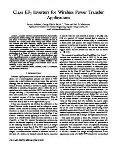
Standard drivers are built according to architecture in Fig.1. It contains usually an output stage, secondary logic, protection circuits and secondary part of insulated power source on the secondary side (side of power transistor). On the primary side there are primary parts of power source and primary logic. The control PWM signal and power supply are transferred through the insulation barrier to the secondary side and transistor/driver error signal is transferred to the primary side. Insulation barrier has to have high du/dt immunity, low parasitic capacity and static insulating capability according to the application field of the drive. These barriers are usually realized by using Optoisolotor or signal transformers [6][7]. There are other possibilities of insulation barrier realization as mentioned in [8] where it used a printed transformer which insulates voltage of 10KV. In [9] [10] was proposed a wireless transmission of switch control information. An opto-coupler is designed to withstand a very high voltage (500V to 10kV) between its input and output.
I. INTRODUCTION The electric drives diagnosis has increasing importance during past years. The reason are increasing requirements on drives reliability and avoiding critical failures by planning of well-timed maintenance. The next requirement is determination of which part of the system is going to a failure or has failed and is necessary to repair or replace. Because of complexity to motor control designs, programmable logic control has quickly increased. Engineers largely use microcontrollers to build a motor control system; sometimes the designers have to use several microcontrollers to complete the design which needs additional functions and this will be expensive. If the design has been completed, the stress of designers will stay in what functionality they can add to the control system and maybe they can’t add any function. So the microcontroller is going to disappear with the appearance FPGA. With an FPGA, the designer can add all control system features to a single chip and even add new functions after he has completed this control system. The electric drive is a system, which can be divided into several parts: driven mechanical system including bearing and gearboxes, electric motor, power inverter, which can be subdivided onto power semiconductor devices, transistor drivers, control circuits, sensors, communication interface and software. A lot of papers have been published and discussed the diagnosis methods for these parts [1][2][3][4]. This paper focuses into the field of power inverter diagnosis. The implementation of diagnostics methods,
Power transistors used in inverters need to be protected from failure. If we understand the power transistor driver as a key part, which directly touches the transistor, it is clear that only in this place it is possible to watch the phenomena that is going to failure of transistor. Monitoring and evaluating of these processes allow performing of very comfortable and circumspective control of state transistor and also allow monitoring of technical state of the transistor and course of downgrading its parameters [5].
II.
The most of diagnostics strategies for inverter can detect proper IGBT operation or its failure [11][12]. Failure in the case of IGBT means permanent switched on state (short circuit) or permanent off state (open circuit) regardless on the switching signal into the driver input. Mostly no methods exist for continuous monitoring of inverter switching transistor condition or other parts of power inverter such as DC link capacitance, leakage resistance, or terminals contact resistances etc. Diagnostics methods for continuous condition monitoring, which was developed for mechanical vibration monitoring or for partial discharges in
This work was supported by the European Regional Development Fund under project No. CZ.1.05/2.1.00/01.0014 and by the faculty project FEKT-S-11-14 “Utilization of new technologies in the power electronics”.
978-1-4799-0224-8/13/$31.00 ©2013 IEEE
FUNDAMENTAL OF PROPOSED IGBT DIAGNOSTIC STRATEGY
785
motor windings etc. doesn’t exists for IGBT transistors proper operation.
III.
ARCHITECTURE OF PROPOSED IGBT DRIVER
The quality of switching process is possible to observe only on transients, when transistor switches on or off. Many influences affect the switching transient in the transistor – transistor switching speed, gate resistance, gate current, dc link capacitance, snubbers capacitance, etc. The measurable quantities are drain-source voltage VDS, gate-source voltage VGS and gate current IG. These quantities are only measurable in the transistor driver in inverter. For this purpose is designed a driver architecture which allows this functionality. Transients of measured quantities can be evaluated and quality of switching process can be monitored. Two approaches can be used for switching process quality monitoring: a) Transient shapes attribute evaluation Transient shapes attributes which can be evaluated can be VDS overshoot, VDS or VGS rise or fall time etc. For this purpose is possible to realize dedicated electronic circuits such as peek detectors, differentiators [5] for observed quantities and separately measure its individual attributes by ADCs with low demands on sampling frequency. Values or changes of particular attributes can point on particular parameters degradation. b) Transient evaluation in frequency or time-frequency domain Transients of observed values can be recorded into memory and mathematical methods can be applied on these records. Assumed mathematical methods are Fourier or wavelet transformation. Outputs of these methods are frequency or time frequency spectrum. We assume that sizes of some selected bars and their combination and relations in these spectrums depend on some IGBT or other parts inverter parameters degradation. These dependencies and relations with IGBT degradation processes should be aim of next research. This way of transient analysis can be assumed as general method of inverter diagnostic and can provide data for many inverter failures propagation monitoring. It is clear, transient recording require high speed AD conversion and high speed data processing. FPGA realization is assumed in this case and is described later. The next stage of diagnostics processing is evaluation of obtained data (attributes, spectral bars) regardless if according to point a) or b). These data is input vector to the stage. Outputs vector is evaluated parameters of particular IGBT or whole inverter in actual time. For the multi-input and multi-output stage is suitable neural network or fuzzy-logic observer which will describe dependences of observed parameters on the input data vector. Time courses of these parameters can be recorded in time in next stage. It is assumed that exponential time course of failure propagation is usually expected. Time to reaching critical value of particular parameter can be computed using exponential extrapolation. These computations are useful for failure time prediction or maintenance planning.
Fig.1. Standard driver architecture
From figure 1 the development of the driver architecture is necessary for purposes of proposed diagnostics in the driver. The proposed driver assumes analogue measurements of various quantities on the driver secondary side and transients quantitative evaluation of measured data and storage of their long-time courses for monitoring particular power transistor or driver secondary circuit’s parameters downgrading. Possibility of parameters setting in the driver is also assumed. Threshold values of particular protection circuits and limiting values of long-time monitored quantities are mentioned as driver parameters. We can depend on the previous results from the recent researches in order to build the hardware with specific requirements, Multichannel ADC converter is necessary for digital processing of the measured data. In this case we have to add some programmable devices (FPGA in our work). RAM and FLASH memory are necessary for measured data storage. The next requirement is data transfer in both directions, measured data transferred from gate driver side and the parameter writing in reverse direction are assumed. For this purpose, we have to develop the inverter control interface (in both directions). Now high speed logic isolators can be used for this purpose When we want to use ADC features to measure the quantities on IGBT transistor (IG, VCE, VGE) or any phenomena occurs quickly, it is necessary to perform periodic data transfer each modulation cycle of the inverter and the current measured parameter has to be synchronized with PWM cycle. On other hand, monitored parameters which aren’t important for drive control and which serve for long-time monitoring as IL can be transferred in longer intervals. The figure 2 shows how we can measure the parameters and quantities of driver using ADC features; we assume the analysis of VCE, VGE and IG quantities during switching on and switching off process. The variables courses transient states are performed within short times (2-4 us in high power IGBTs). For variable analysis we assume necessity of 100 to 256
786
samples to be taken into input buffers. One chip FPGA will receive the all data of one power IGBT parameters in power inverter, this chip processes these data saved in the DDR memory and sends the information of switch on/off of IGBT, IL and VCE to main chip FPGA that generates PWM signals to switching drivers of IGBTs inverter. The data received from main chip will also carry information of faults if they happen, then the chip will interrupt the switching and indicates to the fault. In our proposed system we will use seven chip FPGAs, six chips will detect and diagnose the parameters of six IGBTs in power inverter and the seventh chip will be the master the receives results of detection and diagnosis and generates the PWM signals of IGBT drivers.
Fig.3. interface between one IGBT driver and one chip FPGA.
HR I/O banks have I/O pins more than HP banks and the interface voltage of these banks is up to 3.3V. I/O HR banks will receive the data from AD converters. The data that present the transient signals and the signals that quickly happen have to be written and saved in the DDR memory. Separate fault signal is not necessary, because the error information is also transferred through the data interface. But if we want to switch off the other transistors in the same moment when an error occurs in one transistor, it is necessary to separate the fault signals of each transistor in the power inverter.
Fig.2.Scheme of Driver architecture with ADC several measured quantities
The software used in this proposed system will be written in VHDL language. IV.
INTERFACE BETWEEN CHIPS FPGA AND SWITCHING DRIVERS OF IGBT INVERTER
Figure 3 illustrates the interface between one IGBT driver and one chip FPGA. All analogue signals that are coming from driver and IGBT transistor, using sensors and operational amplifiers, will go to AD converters. The number of AD converters depends on number of signals which we want to analyze. Data outputs of AD converter will go to I/O banks in chip FPGA. The proposed chip FPGA will be one from the 7 series FPGAs that are composed of a high-performance (HP) and high-range (HR) I/O banks. HP I/O banks are designed to perform requirements of high speed memory, they will be used to exchange the data and information between the other chips, this data may contain the present state of IGBT transistor, the interface voltage of these banks is up to 1.8V. Fig.4. interface between inverter controllers (seven chips FPGA) and IGBT drivers
787
The PWM signals that drive the switching drivers of IGBT inverter will be generated by the seventh chip FPGA that watches all functions of other chips FPGAs in the same time. The PWM signals have to be insulated by logic isolator for ignore the distortion. The logic device that is proposed in this hardware has a high speed digital I/O ports and it is designed to isolate five digital control signals to/from chip FPGA. Figure 4 shows the proposed diagram of interface between inverter controllers (seven chips FPGA) and IGBT drivers.
a)
The signal (SELECT/SYNC) is used to define begin and the end of data transfer. This signal doesn’t be used when the data transfer in one master-one slave communication, but if this signal is used, the communication will be more reliable and simple. The using of SPI (serial peripheral interface) with SELECT/SYNC creates a synchronous space between the feedback quantities and the modulation cycle period, especially in relation to inverter output currents measured in the driver. V.
b)
DATA EXCHANGE PROTOCOL
Data exchange is realized between inverter control unit (FPGA) and drivers by a simple communication protocol for standard SPI. There are several services required in the data transfer: driver parameters settings and periodic data reading from the driver at each modulation period. Read data can be divided into two groups: Feedback data used for control process (PERIODIC DATA) and data used for long time power transistor and driver secondary side monitoring. These data are called CYCLIC DATA, because they are mixed into periodic frame. Each message contains one issue of cyclic data addressed by inverter control unit. At least two message types are necessary: The first one is constant writing in to driver FLASH memory. The data frame is shown in fig. 5.a. The message, which is sent into the driver, contains data field MESSAGE_ID = WRITE_CONSTANT. The following data field DATA ADDRESS contains address (negotiated index) of written data. The third field contains value of written parameter. Checksum is unavoidable. Driver status (STATUS WORD) is sent back in each type of message. Status word contains status flags of individual protection circuits and limit values over passing. The second message type is data exchange MESSAGE_ID = DATA_EXCHANGE, fig. 5.c.
–
For periodic data exchange in each modulation period there are fields in outgoing data (PERIODIC_DATA1 to PERIODIC_DATAn) reserved. Only the inverter output current is assumed as periodic data. It means that the data packet length is only four words including checksum. Incoming data contains address (index) of desired cyclic data, which value is sent back in outgoing data in next word. In this data frame there is the incoming checksum in penult data field. Therefore when incoming checksum is invalid, it is possible to make invalid also outgoing checksum in the last data field of outgoing data frame. Due to this feature the validity result of complete data transfer in inverter controller is immediately known.
c) Fig.5. Proposed SPI data transfer protocol: a) data frame for writing parameter into driver memory, b) data frame back reading of parameter or an individual variable, c) data frame for periodic data exchange between the driver and inverter controller.
For written data validation it is important to have possibility of backward data reading. For this purpose the next message type – parameter/variable reading (MESSAGE_ID = READ_DATA) fig 5b has been designed. VI. CONCLUSION The paper proposes a new architecture of an IGBT Inverter with switching driver; this architecture performs diagnostic methods of the power IGBTs in power inverter and it also diagnoses the secondary circuits of driver. The system uses chips FPGAs of 7-series FPGA (kintex7XC7K70T) as an inverter controller. It also uses ADC devices whose number depends on the analogue signals which we want to measure for diagnosis, these signals present all quantities and parameters of IGBT transistors and secondary circuits of driver. Data of signals are transferred from ADCs into the inverter controller. These data serve for inverter critical failure prediction and for maintenance planning. This paper also showes the ability of chip FPGA since it has two types I/O banks HP and HR that allow us to interface between ADCs of drivers (HR) from side and between chips from other side. The article also explained data exchange SPI protocol between the inverter controller and drivers, where at least two message types are necessary. In the present time the inverter controller is going to be designed, using chips FPGAs, the scheme of one chip was designed; we will design the first PCB and test it on one IGBT transistor with its switching driver.
788
REFERENCES [1]
[2]
[3]
[4]
[5]
[6]
Bacha, K.; Gossa, M.; Henao, H.; Capolino, G.-A., "A time-frequency method for multiple fault detection in three-phase induction machines," Diagnostics for Electric Machines, Power Electronics and Drives, 2005. SDEMPED 2005. 5th IEEE International Symposium on , vol., no., pp.1,6, 7-9 Sept. 2005. Kiani, M.; Lee, W-J; Kenarangui, R.; Fahimi, B., "Frequency Domain Methods for Detection of Rotor Faults in Synchronous Machines under No-Load Condition," Power Symposium, 2007. NAPS '07. 39th North American , vol., no., pp.31,36, Sept. 30 2007-Oct. 2 2007. O.Ondel, E.Blanco, G.Clerc,”Beyond the diagnosis :the forecast of state system application in an induction machine,” Diagnostics for Electric Machines, power Electronics and Drives, 2007. SDEMPED 2007. IEEE international Symposium on, vol., no.,pp.491-496,6-8 sept.2007. I.Y.Onel, M.E.H.Benbouzid,”Induction Motors Bearing Failures detection and Diagnosis: Park and Concordia Transform Approaches Comparative Study,” Electric Machines and drives Conference, 2007. IEMDC’07. IEEE International, vol.2, no.,pp.1073-1078,3-5 May 2007. J.Knobloch, B.Klima, Z.Nouman,” Implementation of Diagnostics functions in IGBT drivers, part1,” Diagnostics for Electric Machines, power Electronics & drives (SDEMPED), 2011 IEEE International Symposium on,pp.145-148, 5-8 sept.2011. R.Herzer, S.Pawel, J.Lehmann,” IGBT driver chipset for high power applications,” Power Semiconductor Devices and ICs, 2002. Proceedings of the 14th International Symposium on, pp.161-164, 2002.
[7]
L.Dulau, S.Pontarollo, A.Boimond, J.F.Garnier, N.Giraudo, O.Terrasse, “A new gate driver integrated circuit for IGBT devices with advanced protections,” Power Electronics, IEEE Transactions on, Vol.21,no.1, pp.38-44, Jan.2006. [8] G.Schmitt, W.Kusserow, R.Kennel,” Power Supply for IGBT driver with high insulation voltage based on printed plannar transformers,” Power Electronics and Motion control Conference, 2008, EPE-PEMC 2008. 13Th , PP.1239-1242, 1-3 Sept.2008. [9] C.Batard, G.Andrieux, N.Ginot M.A.Mannah,”Wireless Transmission of IGBT Driver Control,” Applied Power Eectronics Conference and Exposition,2009, APEC 2009. Twenty-Fourth Annual IEEE, pp.12571262, 15-19 Feb.2009. [10] S.Brehaut, F.Costa,” Gate driving of high power IGBT by wireless transmission,” International power Electronics Motion Control,2006,5th IEEE IPEMC 2006. Conference record of the 2006 IEEE, Shanghai, China, 13-16 august 2006, page 1-5, Vol.1. [11] Rodríguez-Blanco, M.A.; Claudio-Sánchez, A.; Theilliol, D.; VelaValdés, L.G.; Sibaja-Terán, P.; Hernández-González, L.; AguayoAlquicira, J., "A Failure-Detection Strategy for IGBT Based on GateVoltage Behavior Applied to a Motor Drive System," Industrial Electronics, IEEE Transactions on , vol.58, no.5, pp.1625,1633, May 2011 [12] Rothenhagen, K.; Fuchs, F.W., "Performance of diagnosis methods for IGBT open circuit faults in voltage source active rectifiers," Power Electronics Specialists Conference, 2004. PESC 04. 2004 IEEE 35th Annual , vol.6, no., pp.4348,4354 Vol.6, 20-25 June 2004
789
Powered by TCPDF (www.tcpdf.org)