FSK Modulation and. Demodulation With the. MSP430 Microcontroller.
December 1998. Mixed-Signal Products. Application. Report. SLAA037 ...
FSK Modulation and Demodulation With the MSP430 Microcontroller
Application Report
December 1998
Mixed-Signal Products SLAA037
IMPORTANT NOTICE Texas Instruments and its subsidiaries (TI) reserve the right to make changes to their products or to discontinue any product or service without notice, and advise customers to obtain the latest version of relevant information to verify, before placing orders, that information being relied on is current and complete. All products are sold subject to the terms and conditions of sale supplied at the time of order acknowledgement, including those pertaining to warranty, patent infringement, and limitation of liability. TI warrants performance of its semiconductor products to the specifications applicable at the time of sale in accordance with TI’s standard warranty. Testing and other quality control techniques are utilized to the extent TI deems necessary to support this warranty. Specific testing of all parameters of each device is not necessarily performed, except those mandated by government requirements. CERTAIN APPLICATIONS USING SEMICONDUCTOR PRODUCTS MAY INVOLVE POTENTIAL RISKS OF DEATH, PERSONAL INJURY, OR SEVERE PROPERTY OR ENVIRONMENTAL DAMAGE (“CRITICAL APPLICATIONS”). TI SEMICONDUCTOR PRODUCTS ARE NOT DESIGNED, AUTHORIZED, OR WARRANTED TO BE SUITABLE FOR USE IN LIFE-SUPPORT DEVICES OR SYSTEMS OR OTHER CRITICAL APPLICATIONS. INCLUSION OF TI PRODUCTS IN SUCH APPLICATIONS IS UNDERSTOOD TO BE FULLY AT THE CUSTOMER’S RISK. In order to minimize risks associated with the customer’s applications, adequate design and operating safeguards must be provided by the customer to minimize inherent or procedural hazards. TI assumes no liability for applications assistance or customer product design. TI does not warrant or represent that any license, either express or implied, is granted under any patent right, copyright, mask work right, or other intellectual property right of TI covering or relating to any combination, machine, or process in which such semiconductor products or services might be or are used. TI’s publication of information regarding any third party’s products or services does not constitute TI’s approval, warranty or endorsement thereof.
Copyright 1998, Texas Instruments Incorporated
Contents 1 Introduction . . . . . . . . . . . . . . . . . . . . . . . . . . . . . . . . . . . . . . . . . . . . . . . . . . . . . . . . . . . . . . . . . . . . . . . . . . . . . . . . . . . 1 2 Demodulation Theory . . . . . . . . . . . . . . . . . . . . . . . . . . . . . . . . . . . . . . . . . . . . . . . . . . . . . . . . . . . . . . . . . . . . . . . . . . 2.1 Choosing the Sampling Rate . . . . . . . . . . . . . . . . . . . . . . . . . . . . . . . . . . . . . . . . . . . . . . . . . . . . . . . . . . . . . . . 2.2 Front End Processing . . . . . . . . . . . . . . . . . . . . . . . . . . . . . . . . . . . . . . . . . . . . . . . . . . . . . . . . . . . . . . . . . . . . . 2.3 FSK Demodulation . . . . . . . . . . . . . . . . . . . . . . . . . . . . . . . . . . . . . . . . . . . . . . . . . . . . . . . . . . . . . . . . . . . . . . . . 2.4 Bit Synchronization . . . . . . . . . . . . . . . . . . . . . . . . . . . . . . . . . . . . . . . . . . . . . . . . . . . . . . . . . . . . . . . . . . . . . . .
2 2 2 2 3
3 Modulation Theory . . . . . . . . . . . . . . . . . . . . . . . . . . . . . . . . . . . . . . . . . . . . . . . . . . . . . . . . . . . . . . . . . . . . . . . . . . . . . 3.1 Choosing the Sampling Rate . . . . . . . . . . . . . . . . . . . . . . . . . . . . . . . . . . . . . . . . . . . . . . . . . . . . . . . . . . . . . . . 3.2 Constructing the Look Up Table . . . . . . . . . . . . . . . . . . . . . . . . . . . . . . . . . . . . . . . . . . . . . . . . . . . . . . . . . . . . 3.3 FSK Modulation . . . . . . . . . . . . . . . . . . . . . . . . . . . . . . . . . . . . . . . . . . . . . . . . . . . . . . . . . . . . . . . . . . . . . . . . . .
4 4 4 4
4 Data Conversion . . . . . . . . . . . . . . . . . . . . . . . . . . . . . . . . . . . . . . . . . . . . . . . . . . . . . . . . . . . . . . . . . . . . . . . . . . . . . . . 5 4.1 A/D Conversion . . . . . . . . . . . . . . . . . . . . . . . . . . . . . . . . . . . . . . . . . . . . . . . . . . . . . . . . . . . . . . . . . . . . . . . . . . 5 4.2 D/A Conversion . . . . . . . . . . . . . . . . . . . . . . . . . . . . . . . . . . . . . . . . . . . . . . . . . . . . . . . . . . . . . . . . . . . . . . . . . . 5 5 Power Consumption . . . . . . . . . . . . . . . . . . . . . . . . . . . . . . . . . . . . . . . . . . . . . . . . . . . . . . . . . . . . . . . . . . . . . . . . . . . 6 6 Exercising the Software . . . . . . . . . . . . . . . . . . . . . . . . . . . . . . . . . . . . . . . . . . . . . . . . . . . . . . . . . . . . . . . . . . . . . . . . 7 6.1 FSK Receiver . . . . . . . . . . . . . . . . . . . . . . . . . . . . . . . . . . . . . . . . . . . . . . . . . . . . . . . . . . . . . . . . . . . . . . . . . . . . 7 6.2 FSK Transmitter . . . . . . . . . . . . . . . . . . . . . . . . . . . . . . . . . . . . . . . . . . . . . . . . . . . . . . . . . . . . . . . . . . . . . . . . . . 7 7 Example Circuits . . . . . . . . . . . . . . . . . . . . . . . . . . . . . . . . . . . . . . . . . . . . . . . . . . . . . . . . . . . . . . . . . . . . . . . . . . . . . . . 8 7.1 Using the MSP430C325 as Main Processor . . . . . . . . . . . . . . . . . . . . . . . . . . . . . . . . . . . . . . . . . . . . . . . . . . 8 7.2 Example Telephone Interface . . . . . . . . . . . . . . . . . . . . . . . . . . . . . . . . . . . . . . . . . . . . . . . . . . . . . . . . . . . . . . 8 8 Summary . . . . . . . . . . . . . . . . . . . . . . . . . . . . . . . . . . . . . . . . . . . . . . . . . . . . . . . . . . . . . . . . . . . . . . . . . . . . . . . . . . . . . 10 9 References . . . . . . . . . . . . . . . . . . . . . . . . . . . . . . . . . . . . . . . . . . . . . . . . . . . . . . . . . . . . . . . . . . . . . . . . . . . . . . . . . . . 11 Appendix A FSK Receiver Routine . . . . . . . . . . . . . . . . . . . . . . . . . . . . . . . . . . . . . . . . . . . . . . . . . . . . . . . . . . . . . . A-1 Appendix B FSK Transmitter Routine . . . . . . . . . . . . . . . . . . . . . . . . . . . . . . . . . . . . . . . . . . . . . . . . . . . . . . . . . . . B-1
List of Figures 1 Main Processor and A/D Converter . . . . . . . . . . . . . . . . . . . . . . . . . . . . . . . . . . . . . . . . . . . . . . . . . . . . . . . . . . . . . . . . . 8 2 Telephone Interface . . . . . . . . . . . . . . . . . . . . . . . . . . . . . . . . . . . . . . . . . . . . . . . . . . . . . . . . . . . . . . . . . . . . . . . . . . . . . . 9
List of Tables 1 FSK Transceiver Performance . . . . . . . . . . . . . . . . . . . . . . . . . . . . . . . . . . . . . . . . . . . . . . . . . . . . . . . . . . . . . . . . . . . . . 9
FSK Modulation and Demodulation With the MSP430 Microcontroller
iii
iv
SLAA037
FSK Modulation and Demodulation With the MSP430 Microcontroller ABSTRACT This application report describes a software program for performing V.23 FSK modem transceiver functions using an MSP430 microcontroller. It makes use of novel filter architecture to perform DSP functions on a processor with only shift and add capabilities.
1 Introduction Many measurement applications (for example, electric and gas meters) require a way to communicate electronically with a central office so that measured data can be reported back to the central office and new tariffs can be set in the remote site. Telephony provides a convenient means of data communication. Frequency shift keying (FSK) and dual tone multi frequency (DTMF) are two popular methods of representing binary data over telephone circuits. This application report describes a V.23-compliant FSK transceiver software module. Integrating the measurement and communication functions onto the same chip yields cost as well as power-saving benefits. Using the MSP430, a high MIPs ultra low power microprocessor, allows power to be drawn from the telephone line in some cases. This report describes the mathematical formulas for FSK signal transmission and detection. A list of the software modules is included with a reference schematic for telephone interface and low cost A/D converter. The schematic is only a reference, since the precise implementation can vary from country to country.
1
Demodulation Theory
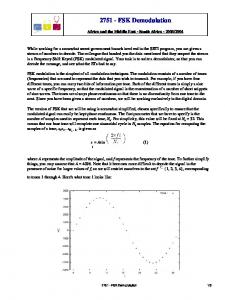
2 Demodulation Theory A quadrature demodulator provides the FSK demodulation. In this type of demodulation, the signal and its delayed version are multiplied together and then low-pass filtered. If the delay, T, is set such that Wcarrier × T = π/2, then the low-pass filter result is proportional to the frequency deviation from the carrier and therefore represents the bit value sent.
+
If w Wcarrier where w = 2π × f :
³
" Wdelta and T
+ "
+
Wcarrier
+ pń2
) cos(2wt–wT) ³ Low Pass Filter +" sin[Wdelta ]
cos[ wt ].cos[w( t–T )] coswT coswT sin[ Wdelta]
2.1
Choosing the Sampling Rate
�
The sampling is chosen to be Fcarrier 4 for the purpose of obtaining the delayed sample without computational overhead. For V.23, the F carrier frequency is 1700 Hz and therefore the sampling rate becomes 6800 Hz. Using a 32768-Hz crystal yields 6793.3 Hz, which is 0.1% out. The sampling frequency is set by the 8-bit interval timer. Because this timer is limited to 256 counts, the interrupt rated is set to twice the sampling rate and the processing is divided into two halves with signal sampling performed every other interrupt.
2.2
Front End Processing Most A/D converters, including the successive approximation A/D converter in the MSP430C325, need a dc bias; this yields an unsigned integer sample with an offset. Before this sample can be processed further, it needs to go through an unbias filter to take out the dc bias and turn the sample into a signed integer value. This unbias filtering also gives 30 dB or so of rejection for main frequencies.
2.3
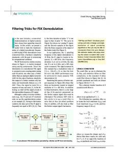
FSK Demodulation The signed integer sample and its delayed version are multiplied together; in this application, an 8×8 signed multiplication loop is used. The product, made up of two frequency elements, is low-pass filtered to remove the double frequency element. The remainder is a signed integer value representing the original bit value transmitted. The low-pass filter uses the digital wave filtering technique. This technique gives stable characteristics with very good coefficient tolerance. All multiplication is done through shifts and adds with the number of shift/add operations minimized through rounding off the coefficients. Because the filter has good coefficient tolerance, this rounding off does not affect the filter performance. The Butterworth filter used here gives approximately 40-dB attenuation in the stop band with 1-dB pass and ripple.
2
SLAA037
Demodulation Theory
2.4
Bit Synchronization The bit values coming out from demodulation need to be determined and synchronized to produce the incoming data bit stream. This process is also known as bit slicing and clock recovery. Because the sampling rate at 6800 is not an integer multiple of the data rate (baud rate) at 1200, an additional step is needed to consolidate between the two rates. This is done through a count-down counter with a sequence of preload value (5,6,5). Every 17 samples, the sampling rate and the data baud rate are resynchronized. Bit synchronization or clock recovery is done by monitoring bit value transitions. Lead or lag information is then obtained and the count-down counter is adjusted accordingly. Because of the difference between the sampling clock and the data clock, the data bit is never sampled at the middle of the baud period; instead a –5% to 13% variation is introduced. However, this should not have any adverse effect on the accuracy of the system, as it has been verified experimentally.
FSK Modulation and Demodulation With the MSP430 Microcontroller
3
Modulation Theory
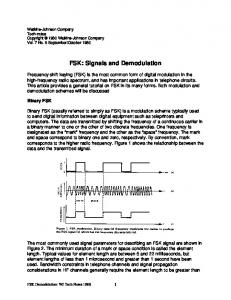
3 Modulation Theory FSK modulation involves alternating the value of a delta frequency from a carrier frequency according to the value of the bit to be represented. For V.23, a bit value of 0 = 400 Hz and a bit value of 1 = –400 Hz.
FSK signal
+ Amplitude
cos[t| 2p
( Fcarrier
" Fdelta )]
The sinusoidal signal is generated through a lookup table which contains cosine values from 0 to 2π. A parameter called PHASER (16 bit) represents the current angle: 0=0 degree, 8000 hex = 180 degree 10000 hex = 360 degree. With each sample, this angle is advanced by another parameter DELTA (16 bit) which determines the frequency of the signal (larger DELTA value = higher frequency). Frequency modulation is realized by changing the DELTA value according to the bit value to be transmitted at each baud period, according to the following formula:
DELTA
+ FdesiredńFsampling
65536.
The advantage of this method over a digital oscillator method is that this method preserves the phase relationship even when the frequency is shifted from sample to sample.
3.1
Choosing the Sampling Rate The 8-bit interval timer sets the sampling rate to 19200 samples/s. This rate is subdividable into the data baud rate of 1200. Also, it is sufficiently high to make the D/A process simpler.
3.2
Constructing the Look Up Table To save ROM space, only the first quadrant (0 to 127 degrees) in Q7 format is coded. This is done by dividing the first quadrant (90 degrees) into 128 steps of approximately 0.7 degrees each. The remaining three quadrants can be worked out from this first quadrant table using additional computation.
3.3
FSK Modulation The parameter PHASER is advanced by the amount DELTA at every interrupt. The first 9 bits of the PHASER is used to look up the cosine value. For the cosine function, the third and fourth quadrant are the same as the second and first quadrant, and so only the absolute value of the first 9 bits of PHASER is used. Next, all second quadrant values are derived from the first quadrant ROM table. The 8-bit result value is stored onto P0.OUT. Every 16 interrupts, the parameter DELTA is updated with the next frequency by looking at the next bit to be transmitted.
4
SLAA037
Data Conversion
4 Data Conversion This section describes the required digital-to-analog (D/A) and analog-to-digital (A/D) data conversions.
4.1
A/D Conversion The most straightforward way to digitize the incoming FSK signal is to use the 12-bit mode of the internal 14-bit A/D converter of the MSP430C325. However, not all of the 12 bits are needed to achieve good dynamic range for the FSK demodulation. Simulation results indicate that an 8-bit A/D stage gives good dynamic range up to 25 dB using internal AGC software. With an additional external AGC stage, the dynamic range can be further widened. As economical means of building 8-bit single slope A/D exists, this extends the application of this module to the rest of the MSP430 family. The application software included here uses a single slope A/D (universal timer with external comparator) for the demodulator. This makes the software universally applicable for the whole family.
4.2
D/A Conversion A 6-bit external R–2R ladder is used to construct the D/A converter. Because the carrier frequency of 19200 Hz is nine times the highest frequency of the FSK of 2100 Hz, the post filtering stage should be relatively simple. In the application circuit, a single capacitor forms a single pole low pass filter but more poles can be realized using additional passive networks.
FSK Modulation and Demodulation With the MSP430 Microcontroller
5
Power Consumption
5 Power Consumption The FSK concept is designed with low power in mind. The FSK demodulator takes less than 2 MIPs. With a low power op-amp as a front-end, total power consumption of less that 1.5 mA should be achievable. Thus, it is possible that the power can be derived entirely from the telephone line. A schematic is included for a suggested telephone line interface. The precise configuration may vary from country to country.
6
SLAA037
Exercising the Software
6 Exercising the Software This section describes operation of the software.
6.1
FSK Receiver The FSK signal is derived from the telecom interface circuit. This signal should have a dc bias of 1.2 V and a peak-to-peak level of 400 mV. The software decodes this FSK signal and produces three outputs which lets the user monitor the demodulated data. • TP.3. This is the clock signal recovered from the input FSK. • TP.5. This is the data recovered from the input FSK; data is latched out every rising edge of TP.3. • P0.2–P0.7. These six bits output the low pass filtered result. With an external R–2R ladder this becomes very useful in monitoring the analogue FSK demodulator output level. It is hard limited to 8 bits with the MSB 6 bits loaded to port P0
6.2
FSK Transmitter The transmitter software outputs an FSK signal according to the BIT MAP data defined in TX_DATA_TABLE. The bitmap pattern starts with a preamble followed by a long MARK period. Then the actual data is transmitted. This table uses a zero word as an end marker, and the software restarts the whole data sequence upon reaching a zero value in the bit map data.
FSK Modulation and Demodulation With the MSP430 Microcontroller
7
Example Circuits
7 Example Circuits This section shows and describes example circuits.
7.1
Using the MSP430C325 as Main Processor Figure 1 shows an example circuit using the MSP430C325 as the main processor. The circuit is tested with 400 mV peak-to-peak FSK input. To obtain the same results, Rx needs to be biased at 1.2 V with a 400 mV peak-to-peak FSK signal superimposed. VSS R1 R2
PO.2 PO.3 PO.4 PO.5 PO.6 PO.7
MSP430E325 TP.5
RX_DATA
TP.1 TP.4 CIN TP.3 RX_CLK
4066
Line Interface RX TX Hook
1
A
B
2
C 13 VCC 1N4148 33 kΩ
6 _
Voltage Ramp
5
7
+
PNP Sample_Hold NPN
1 nF
Figure 1. Main Processor and A/D Converter
7.2
Example Telephone Interface Figure 2 shows an example telephone interface, and Table 1 lists FSK transceiver performance data.
8
SLAA037
Example Circuits
Telephone Line A B 33 nF
20 kΩ 1 µF +
TX
1 kΩ
TLC2279 6 _
1 kΩ
5
VREF (1.5 V)
500 Ω
7
+ 6–8 V Zeners
33 kΩ 20 kΩ 20 kΩ 20 kΩ
9 _
10 kΩ
10
Tuning For Minimum Side Tone
DC Telephone Isolation Transformer
6–8 V Zeners
8
+
150 kΩ 400 mV pk–pk RX
1 µF
14
+
– +
33 kΩ
13
33 kΩ
12
680 Hook 150 kΩ
This is a reference circuit only and may not be applicable under some circumstances. Figure 2. Telephone Interface Table 1. FSK Transceiver Performance RAM (BYTES)
ROM (BYTES)
FSK Receiver
18
512
MIPS (APPROX.) 2
FSK Transmitter
12
400
1.4
FSK Modulation and Demodulation With the MSP430 Microcontroller
9
Summary
8 Summary FSK transceivers are normally realized by either analog means or by the use of DSPs with hardware MAC units. Using an MSP430 RISC processor without a hardware MAC to achieve the transceiver function is a very unusual approach. The ability to create filters using digital wave filtering techniques, together with the orthogonal instruction set and the 16 bit architecture of the MSP430, makes the code very ROM and MIPs efficient. Moreover, the ultra low power capability of the MSP430 means that power can readily be derived from the phone line. This leads to component-efficient designs. The author has conducted other tests to conclude that, with some enhancements, the FSK receiver can work with an 8-bit A/D converter with enough sensitivity. Therefore the FSK transceiver can be implemented economically across the whole MSP430 family.
10
SLAA037
References
9 References 1. Texas Instruments: MSP430 Family, Architecture User’s Guide and Module Library. 2. Texas Instruments Digital Signal Processing Application with the TMS320 Family Volume 2. 3. Gaszi, L: Explicit Formulas for Lattice Wave Digital Filters; IEEE Trans. On Circuits and Systems VOL. CAS-32, NO. 1, January 1985
FSK Modulation and Demodulation With the MSP430 Microcontroller
11
12
SLAA037
FSK Receiver Routine
Appendix A CPUOFF SCG0 SCG1 IE1 IE1_P0IE1 IE1_P0IE0 IE1_OFIE IE1_WDTIE IE2 IE2_BTIE IE2_TPIE IE2_ADIE IE2_UTXRIE IE2_URXIE IFG1 IFG1_2 IFG2 ME1 ME2 P0IN P0OUT P0DIR P0FLG P0IES P0IE LCDCTL LCDM BTCTL BTCTL_SSEL BTCTL_Hold BTCTL_DIV BTCTL_FREQ1 BTCTL_FREQ0 BTCTL_IP2 BTCTL_IP1 BTCTL_IP0 BTCNT1 BTCNT2 BTIFG TCCTL TCCTL_SSEL1 TCCTL_SSEL0 TCCTL_ISCTL TCCTL_TXE TCCTL_ENCNT TCCTL_RXACT TCCTL_TXD TCCTL_RXD TCPLD TCDAT TPD TPD_B16 TPD_CPON TPE TPE_0 TPE_1 TPE_2 TPE_3
.equ .equ .equ .equ .equ .equ .equ .equ .equ .equ .equ .equ .equ .equ .equ .set .equ .equ .equ .equ .equ .equ .equ .equ .equ .equ .equ .equ .equ .equ .equ .equ .equ .equ .equ .equ .equ .equ .equ .equ .equ .equ .equ .equ .equ .equ .equ .equ .equ .equ .equ .equ .equ .equ .equ .equ .equ .equ
FSK Receiver Routine 010h 040h 080h 0h 08h 04h 02h 01h 01h 80h 08h 04h 02h 01h 02h 04h 03h 04h 05h 010h 011h 012h 013h 014h 015h 030h 030h 040h 80h 40h 20h 10h 08h 04h 02h 01h 046h 047h 080h 042h 080h 040h 020h 010h 008h 004h 002h 001h 043h 044h 04eh 080h 040h 04fh 01h 02h 04h 08h
; LCD control & mode register address
; BT intrpt flag ; Address of Timer/Counter control register
; Address of Timer/Counter pre–load register ; Address of Timer/Counter
FSK MOdulation and Demodulation With the MSP430 Microcontroller
A-1
FSK Receiver Routine TPE_4 TPE_5 TPE_TPSSEL2 TPE_TPSSEL3 TPCTL TPCTL_EN1FG TPCTL_RC1FG TPCTL_RC2FG TPCTL_EN1 TPCTL_ENA TPCTL_ENB TPCTL_TPSSEL0 TPCTL_TPSSEL1 TPCNT1 TPCNT2 SCFI0 SCFI1 SCFQCTL CBCTL CBE AIN AEN ACTL ACTL_CSTART ACTL_SVCC_OFF ACTL_SVCC_ON ACTL_2 ACTL_3 ACTL_4 ACTL_5 ACTL_SEL_A0 ACTL_SEL_A1 ACTL_SEL_A2 ACTL_I_SRC_A0 ACTL_I_SRC_A1 ACTL_RNG_B ACTL_RNG_AUTO ACTL_POWER_UP ACTL_POWER_DOWN ACTL_CLK_MCLK ACTL_CLK_MCLK_2 ACTL_CLK_MCLK_3 ADAT ADIFG WDTCTL WDTHold WDT_wrkey STACK
.equ .equ .equ .equ .equ .equ .equ .equ .equ .equ .equ .equ .equ .equ .equ .equ .equ .equ .equ .set .equ .equ .equ .equ .equ .equ .equ .equ .equ .equ .equ .equ .equ .equ .equ .equ .equ .equ .equ .equ .equ .equ .equ .equ .equ .equ .equ .set
10h 20h 40h 80h 04Bh 01h 02h 04h 08h 10h 20h 40h 80h 04Ch 04Dh 050h 051h 052h 053h 1 0110h 0112h 0114h 0001h 0000h 0002h 0004h 0008h 0010h 0020h 0000h 0004h 0008h 0000h 0040h 0200h 0800h 0000h 1000h 0000h 2000h 4000h 0118h 04h 0120h 80h 05A00h 300h ;280h start of system stack
*********************************************** * Filters *********************************************** WDF_PARMS .usect ”FILTMEM”,10,0200h IN_Z .set 0 Z1_1 .set 2 Z1_2 .set 4 Z3_1 .set 6 Z3_2 .set 8 end_of_parms .usect ”FILTMEM”,2 data_word .usect ”FILTMEM”,2 last_sample .usect ”FILTMEM”,2 A-2
SLAA037
FSK Receiver Routine bit_lead_lag cycle_counter
.usect ”FILTMEM”,2 .usect ”FILTMEM”,1
;user service routine
;**************************************************************** ; These are used during the 8 bit timer interrupt ; for FSK demodulation ;**************************************************************** ************************ * DYNAMIC: The Registers Marked (used by WDF) must not be used moved. ************************ currenty .set R6 ;used by WDF currentx .set R7 ;used by WDF IROP1 .set currenty ;used by WDF IROP2L .set R7 ;used by WDF IRACL .set R8 ;used by WDF IRBT .set R9 ;used by WDF lastx .set R10 bit_data .set R11 ;used by WDF mem_ptr .set R15 ;used by WDF ************************ * STATIC ************************ bit_sync_timer global_status bits_count INTERRUPT_TOGGLE FALLING CLOCK
.set .set .set .set .set .set
R12 R13 R14 1 2 4
; ; ;
;************************************************** ;System Init ;************************************************** ;RAM_NORMAL_DEMOD .sect ”RAM_CODE”,02f0h Start .sect ”ADC”,0f000h ;0214h ;0F000h mov #STACK,SP ;initialize system stack pointer mov #(WDTHold+WDT_wrkey),&WDTCTL ; Stop Watchdog Timer clr.b &IFG1 ;clear all interrupt flags clr.b &IFG2 mov.b #(17*5)–1,&SCFQCTL ;MCLK=32768*17*5 gives 2.8 MIPs mov.b #4,&SCFI0 ;Set RC oscillator to 2xFreq range mov.b #–205,&TCPLD ;328/2 ;reset is lo/hi edge bis.b #TPD_B16,&TPD ;op–amp bis.b #11111110b,&P0DIR ;set P0.7–P0.1 to output ;P0.0 used for RING mov.b #(TCCTL_SSEL1+TCCTL_ISCTL+TCCTL_ENCNT),&TCCTL bic.b #IE2_BTIE,&IE2 ;disable Basic Timer Interrupt bic.b #IE1_P0IE0,&IE1 ;disable P0.0 interrupt bic.b #IE2_TPIE,&IE2 ;disable Universal timer Interrupt bis.b #TPE_0+TPE_1+TPE_2+TPE_3+TPE_5,&TPE ;TP_0 is used for Hook ;TP_1 is used for RAMP generator control ;TP_2 is used for test circuit ;TP_3 is the recovered clock bit ;TP_5 is the data bit mov #1,bit_sync_timer mov.b #3,cycle_counter call #clear_all_parameters ;