Gallium nitride nanorod arrays as lowrefractive-index transparent media in the entire visible spectral region Hung-Ying Chen,1 Hon-Way Lin,1 Chen-Ying Wu,1 Wei-Chun Chen,2 Jyh-Shin Chen,2 and Shangjr Gwo1,2,* 1
Department of Physics, National Tsing-Hua University Hsinchu 300, Taiwan, Republic of China 2 Instrument Technology Research Center, National Applied Research Laboratories, Hsinchu 300, Taiwan, Republic of China * Corresponding author:
[email protected]
Abstract: Vertically aligned gallium nitride (GaN) nanorod arrays grown by the catalyst-free, self-organized method based on plasma-assisted molecular-beam epitaxy are shown to behave as subwavelength optical media with low effective refractive indices. In the reflection spectra measured in the entire visible spectral region, strong reflectivity modulations are observed for all nanorod arrays, which are attributed to the effects of Fabry-Pérot microcavities formed within the nanorod arrays by the optically flat air/nanorods and nanorods/substrate interfaces. By analyzing the reflectivity interference fringes, we can quantitatively determine the refractive indices of GaN nanorod arrays as functions of light wavelength. We also propose a model for understanding the optical properties of GaN nanorod arrays in the transparent region. Using this model, good numerical fitting can be achieved for the reflectivity spectra. ©2008 Optical Society of America OCIS codes: (160.5320) Photorefractive materials; (160.4236) Thin films, optical
properties; (160.4236) Nanomaterials; (160.6000) Semiconductor Materials; (300.6550) Spectroscopy, visible; (260.2065) Effective medium theory.
References and links 1.
P. B. Clapham and M. C. Hutley, “Reduction of lens reflexion by the ‘moth eye’ principle,” Nature 244, 281−282 (1973). 2. S. J. Wilson and M. C. Hutley, “The optical properties of ‘moth eye’ antireflection surfaces,” Opt. Acta 29, 993−1009 (1982). 3. M. Srinivasarao, “Nano-optics in the biological world: Beetles, butterflies, birds, and moths,” Chem. Rev. 99, 1935−1961 (1999). 4. M. E. Motamedi, W. H. Southwell, and W. J. Gunning, “Antireflection surfaces in silicon using binary optics technique,” Appl. Opt. 31, 4371−4376 (1992). 5. P. Lalanne and G. M. Morris, “Antireflection behavior of silicon subwavelength periodic structures for visible light,” Nanotechnology 8, 53−56 (1997). 6. Y. Kanamori, K. Hane, H. Sai, and H. Yugami, “100 nm period silicon antireflection structures fabricated using a porous alumina membrane mask,” Appl. Phys. Lett. 78, 142−143 (2001). 7. D. E. Aspnes, “Optical properties of thin-films,” Thin Solid Films 89, 249−262 (1982). 8. D. R. Smith, W. J. Padilla, D. C. Vier, S. C. Nemat-Nasser, and S. Schultz, “Composite medium with simultaneously negative permeability and permittivity.” Phys. Rev. Lett. 84, 4184−4187 (2000). 9. D. R. Smith, J. B Pendry, and M. C. K. Wiltshire, “Metamaterials and negative refractive index,” Science 305, 788−792 (2004). 10. J.-Q. Xi, J. K. Kim, and E. F. Schubert, “Silica nanorod-array films with very low refractive indices,” Nano Lett. 5, 1385−1387 (2005). 11. J.-Q. Xi, J. K. Kim, E. F. Schubert, D. Ye, T.-M. Lu, and S.-Y. Lin, “Very low-refractive-index optical thin films consisting of an array of SiO2 nanorods,” Opt. Lett. 31, 601−603 (2006). 12. J.-Q. Xi, M. F. Schubert, J. K. Kim, E. F. Schubert, M. Chen, S.-Y. Lin, W. Liu, and J. A. Smart, “Optical thin-film materials with low refractive index for broadband elimination of Fresnel reflection,” Nat. Photonics 1, 176−179 (2007).
#93615 - $15.00 USD
(C) 2008 OSA
Received 10 Mar 2008; revised 1 May 2008; accepted 1 May 2008; published 20 May 2008
26 May 2008 / Vol. 16, No. 11 / OPTICS EXPRESS 8106
13. C.-H. Hsu, H.-C. Lo, C.-F. Chen, C. T. Wu, J.-S. Hwang, D. Das, J. Tsai, L.-C. Chen, and K.-H. Chen, “Generally applicable self-masked dry etching technique for nanotip array fabrication,” Nano Lett. 4, 471−475 (2004). 14. Y.-F. Huang, S. Chattopadhyay, Y.-J. Jen, C.-Y. Peng, T.-A. Liu, Y.-K. Hsu, C.-L. Pan, H.-C. Lo, C.-H. Hsu, Y.-H. Chang, C.-S. Lee, K.-H. Chen, and L.-C. Chen, “Improved broadband and quasi-omnidirectional anti-reflection properties with biomimetic silicon nanostructures,” Nat. Nanotechnol. 2, 770−774 (2007). 15. H.-Y. Chen, H.-W. Lin, C.-H. Shen, and S. Gwo, “Structure and photoluminescence properties of epitaxially oriented GaN nanorods grown on Si (111) by plasma-assisted molecular-beam epitaxy,” Appl. Phys. Lett. 89, 243105 (2006), and references therein. 16. E. F. Schubert, Light-Emitting Diodes, 2nd Edition (Cambridge University Press, Cambridge, 2006). 17. T. Fujii, Y. Gao, R. Sharma, E. L. Hu, S. P. DenBaars, and S. Nakamura, “Increase in the extraction efficiency of GaN-based light-emitting diodes via surface roughening,” Appl. Phys. Lett. 84, 855−857 (2004). 18. T. N. Oder, K. H. Kim, J. Y. Lin, and H. X. Jiang, “III-nitride blue and ultraviolet photonic crystal light emitting diodes,” Appl. Phys. Lett. 84, 466−468 (2004). 19. J. J. Wierer, M. R. Krames, J. E. Epler, N. F. Gardner, M. G. Craford, J. R. Wendt, J. A. Simmons, and M. M. Sigalas, “InGaN/GaN quantum-well heterostructure light-emitting diodes employing photonic crystal structures,” Appl. Phys. Lett. 84, 3885−3887 (2004). 20. A. David, T. Fujii, R. Sharma, K. McGroddy, S. Nakamura, S. P. DenBaars, E. L. Hu, C. Weisbuch, and H. Benisty, “Photonic-crystal GaN light-emitting diodes with tailored guided modes distribution,” Appl. Phys. Lett. 88, 061124 (2006). 21. J. Y. Kim, T. Gessmann, E. F. Schubert, J.-Q. Xi, H. Luo, J. Cho, C. Sone, and Y. Park, “GaInN lightemitting diode with conductive omnidirectional reflector having a low-refractive-index indium-tin oxide layer,” Appl. Phys. Lett. 88, 013501 (2006). 22. J. Zhong, H. Chen, G. Saraf, Y. Lu, C. K. Choi, J. J. Song, D. M. Mackie, and H. Shen, “Integrated ZnO nanotips on GaN light emitting diodes for enhanced emission efficiency,” Appl. Phys. Lett. 90, 203515 (2007). 23. H.-M. Kim, T. W. Kang, and K. S. Chung, “Nanoscale ultraviolet-light-emitting diodes using wide-bandgap gallium nitride nanorods,” Adv. Mater. 15, 567−569 (2003). 24. H.-M. Kim, Y.-H. Cho, H. Lee, S. I. Kim, S. R. Ryu, D. Y. Kim, T. W. Kang, and K. S. Chung, “Highbrightness light emitting diodes using dislocation-free indium gallium nitride/gallium nitride multiquantumwell nanorod arrays,” Nano Lett. 4, 1059−1062 (2004). 25. A. Kikuchi, M. Kawai, M. Tada, and K. Kishino, “InGaN/GaN multiple quantum disk nanocolumn lightemitting diodes grown on (111) Si substrate,” Jpn. J. Appl. Phys. 43, L1524−L1526 (2004). 26. A. Kikuchi, M. Tada, K. Miwa, and K. Kishino, “Growth and characterization of InGaN/GaN nanocolumn LED,” Proc. SPIE 6129, 612905 (2006). 27. K. Kishino, A. Kikuchi, H. Sekiguchi, and S. Ishizawa, “InGaN/GaN nanocolumn LEDs emitting from blue to red,” Proc. SPIE 6473, 64730T (2007). 28. G. Yu, G. Wang, H. Ishikawa, M. Umeno, T. Soga, T. Egawa, J. Watanabe, and T. Jimbo, “Optical properties of wurtzite structure GaN on sapphire around fundamental absorption edge (0.78−4.77 eV) by spectroscopic ellipsometry and the optical transmission method,” Appl. Phys. Lett.70 3209−3211 (1997); the refractive index n was found to follow the Sellmeir-type dispersion relationship n2(λ) = 2.272 + 304.72/(λ2 − 294.02) with the incident photon energy below the fundamental band edge of wurtzite GaN. 29. T. Kawashima, H. Yoshikawa, S. Adachi, S. Fuke, and K. Ohtsuka, “Optical properties of hexagonal GaN,” J. Appl. Phys. 82, 3528−3535 (1997). 30. H. C. van de Hulst, Light Scattering by Small Particles (Dover Publications, New York, 1981).
1. Introduction The ultimate goal of controlling the properties of optical media is to manipulate their refractive indices, which can alter their behaviors in light reflection, refraction, diffraction, and interference. For semiconductors, the problem of surface reflection is particularly severe because semiconductors have very high values of refractive index in the visible and near infrared spectral regions. For example, in the near-infrared region, the reflection loss of silicon in air is ~30% at normal incidence. Thus, achieving a way to reduce the reflection loss would be of interest for Si-based solar-cell and optoelectronic device applications. At present, there are some possibilities to overcome this problem. For instance, nanostructured periodic or aperiodic surfaces with feature sizes less than the light wavelength have been known to exhibit the antireflective effects of zero-order gratings (also known as the moth-eye effects) [1-6]. Alternatively, there are other approaches utilizing the optical properties of nanocomposite materials. In such type of materials, if the feature sizes of the embedded nanostructures in a composite material are significantly smaller than the wavelength of incident light, the
#93615 - $15.00 USD
(C) 2008 OSA
Received 10 Mar 2008; revised 1 May 2008; accepted 1 May 2008; published 20 May 2008
26 May 2008 / Vol. 16, No. 11 / OPTICS EXPRESS 8107
embedded nanostructures would not be resolved by the light and the composite material behaves as an effective medium with its optical properties interpolated between those of composing materials [7]. Therefore, by varying the filling factor (volume fraction) of the embedded nanostructures, it is possible to control the effective refractive index and engineer new optical materials previously unavailable in nature. Recently, the availability of new nanofabrication technologies and synthesis routes of nanostructured materials have made it possible to consider various artificial subwavelength optical media [8-14]. However, most of the reported subwavelength antireflective structures are made from silicon using lithographic methods [4-6] or other means (e.g., self-masked dry etching technique, see Refs. [13,14]). Here, we demonstrate that vertically aligned gallium nitride (GaN) nanorod arrays prepared by a catalyst-free, self-organized epitaxial growth method [15] can be used as subwavelength structured optical media with low effective refractive indices in the entire visible spectral region. Recently, GaN-based light-emitting diodes (LEDs) and lasers have become the major choice for devices operating in the short wavelength range because of the ambipolar dopability of GaN [16]. One of the remaining challenges for improving GaN-based LEDs is to reduce their optical losses, originating from the high refractive index of GaN (~2.5). For example, to realize general solid-state lighting or full-color display using high-efficiency GaN-based LEDs, it is important to enhance their light extraction efficiency, which is limited by the loss of total internal reflection. For an air/GaN planar interface, the critical angle for total internal reflection is only ~24° and only about 4% (≈1/(4n2), where n is the refractive index of GaN) of the emitting light can escape from the GaN region. There have been extensive ongoing research efforts to improve the light extraction efficiency of GaN-based LEDs, such as surface subwavelength texturing [17] or incorporation of photonic crystals in the LED structures [18-20]. However, these methods might not be practical for large-scale applications due to their complicate and costly lithographic processes. More recently, a new approach has been proposed to enhance light extraction efficiency by using transparent, conductive indium-tin oxide [21] and ZnO [22] nanorod arrays with low effective refractive indices. In comparison with these nanorod materials, GaN nanorod arrays can be doped to be both n- and p-type, and have the same physical and thermal properties as the bulk GaN crystal, making them more suitable and durable for high-power GaN-based optoelectronic applications. Furthermore, it has been shown that incorporation of active regions within the GaN nanorods is a viable approach to fabricate GaN-nanorod-based LEDs [23-27]. The aforementioned characteristics of GaN nanorod arrays make them particularly interesting for future GaN-based light emitting applications as low-refractive-index optical media. 2. Sample growth and optical measurements Vertically aligned, wurtzite GaN nanorod arrays studied here were grown on 3-inch Si(111) wafers by plasma-assisted molecular-beam epitaxy (PA-MBE). The details of growth process can be found elsewhere [15]. The grown GaN nanorod arrays have been confirmed to be single crystalline and epitaxially oriented with the epitaxial relationship of GaN ‖ < 1 10>Si and GaN‖ Si. And, the GaN nanorods are nitrogen-polar with the axial direction pointed to the –c-axis ([000 1 ] direction). The reflectivity spectra were measured using a Perkin-Elmer Lambda 900 spectrophotometer equipped with a tungsten lamp and an integrating sphere/photomultiplier tube for collecting the reflected light. This system was calibrated by a standard aluminum mirror from National Physical Laboratory (NPL, U.K.).
#93615 - $15.00 USD
(C) 2008 OSA
Received 10 Mar 2008; revised 1 May 2008; accepted 1 May 2008; published 20 May 2008
26 May 2008 / Vol. 16, No. 11 / OPTICS EXPRESS 8108
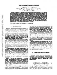
Fig. 1. FE-SEM images of the vertically aligned GaN nanorod arrays grown on Si(111) by PAMBE. Plan view (upper panels) and cross-sectional (lower panels) view of (a) 0.4 μm, (b) 1.2 μm, and (c) 2 μm GaN nanorod arrays.
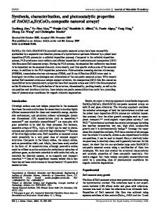
Fig. 2. Normal-incidence reflectivity spectra of vertically-aligned GaN nanorod arrays. The dashed line labels the incident photon energy that corresponds to the GaN band gap energy. To the left of the dashed line is the opaque region, and to the right of the dashed line is the transparent region. The dotted curves in the opaque region are the reflectivities of GaN epilayers measured with the same set-up.
#93615 - $15.00 USD
(C) 2008 OSA
Received 10 Mar 2008; revised 1 May 2008; accepted 1 May 2008; published 20 May 2008
26 May 2008 / Vol. 16, No. 11 / OPTICS EXPRESS 8109
3. Results and discussion Figure 1 shows the field-emission scanning electron microscope (FE-SEM) images in the plan and tilted views of GaN nanorods with different plasma-assisted molecular-beam epitaxy (PAMBE) growth times, corresponding to the rod lengths of 0.4 μm, 1.2 μm, and 2 μm, respectively. In the tilted view of GaN nanorods, no significant lateral growth of individual nanorods can be found. We also find that the mean diameter and aerial density of GaN nanorods depend on the growth temperature and III/V ratio, whereas the nanorod height mainly depends on the growth time. Analyzing from the FE-SEM images, independent of the nanorod length, the PA-MBE-grown GaN nanorods exhibit a uniform mean diameter of ~40 nm (standard deviation ~20 nm) and an aerial density of ~5×1010 cm−2. Moreover, the height of GaN nanorods appears to be quite uniform, forming an optically flat interface with the ambient air. Thus, the aspect ratio of nanorods can be simply controlled by growth time and the percentage of aerial coverage in the plan view can be regarded as the volume fraction occupied by the GaN nanorods. With increasing growth time (longer nanorod length), individual nanorods gradually coalesce into nanorod bundles on the top region of the GaN nanorod arrays, which can be clearly seen in the tilted-view FE-SEM images. Although the coalescence phenomenon becomes serious for the case of long GaN nanorods, the percentage of coverage are 50±5% for all samples. Here, the percentage of nanorod coverage is estimated by analyzing the contrast distributions [gray-scale histograms, ranging from 0 (white) to 255 (black)] in the plan-view FE-SEM images. A threshold gray level, corresponding to the nanorod edges, is selected first. And, the shaded area from zero to the threshold level in the histogram is used to determine the total number of image pixels that GaN nanorods occupy. Therefore, the percentage of coverage can be determined by the ratio of nanorod-occupied pixels to the total pixels in the FE-SEM image. The uncertainty of measurement exists due to the limited image resolution (i.e., boundary sharpness) and limited gray levels. Figure 2 shows the normal-incidence reflectivity spectra in the near-ultraviolet (UV) and visible regions from three GaN nanorod arrays, corresponding to rod lengths of 0.4 μm, 1.2 μm, and 2 μm, respectively. As can be clearly seen in the spectra, when the incident photon energy is larger than the direct band gap energy of GaN (3.4 eV; the wavelength of incident light in air λ < 365 nm), flat and featureless reflectivity spectra are observed. On the contrary, strongly modulated reflectivity spectra are measured when the incident photon energy is below the band gap energy of GaN (in the transparent region). In Fig. 2, the observed reflectivity fringe strongly depends on the rod length of nanorod arrays, suggesting that optical interference might be responsible for the observed reflectivity modulation in the transparent region. Indeed, as will be shown in the following discussion, this phenomenon can be attributed to the effects of Fabry-Pérot microcavities formed within the nanorod arrays by the optically flat air/nanorods and nanorods/substrate interfaces. First of all, we discuss the results of reflectivity measurements in the opaque region, where the incident light can only penetrate a limited depth of GaN nanorod arrays near the air interface. In this probing depth, the effective refractive index can be expressed as a complex number Neff = neff + ikeff and the imaginary part keff is a nonzero real number, which can be used to determine the light absorption coefficient (α = 4πk eff λ ). For GaN, the near-UV light penetration depth is smaller than 100 nm [28]. Thus, the single reflection at the interface between air and GaN nanorod array can be approximated to the total film reflection. By applying the Fresnel equation and nair = 1.0, the normal-incidence reflectivity R= r
2
=
(neff (neff
2 − 1)2 + k eff 2 + 1)2 + k eff
≈
(neff (neff
− 1)2 for photon energy just above the fundamental absorption + 1)2
2 edge ( keff