and positive edge triggered D flip-flop has been represented by using this reversible gate. Afterwards different sequence generators by the sequential elements ...
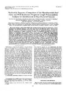
International Journal of Computer Applications (0975 – 8887) Volume 141 – No.1, May 2016
Implementation of Sequence Generator by the Sequential Elements (D-Flip Flop) of Reversible Gates Shefali Mamataj
Saravanan Chandran
Biswajit Das
Murshidabad College of Engineering and Technology, ECE Department, India
NIT,Durgapur Computer Centre, India
Murshidabad College of Engineering and Technology, CSE Department, India
ABSTRACT Power dissipation is a significant factor in the field of today’s electrical or electronic designing. The most promising substitute to these issues is the reversible computing. The reversible circuits do not dissipate energy as much as irreversible circuits. The reversible circuits do not lose information and can also produce unique outputs from the specific inputs and vice versa. So in the view point of designing issues reversible logic is the most important field of research having applications in low power computing, quantum computing, optical computing, and other emerging computing technologies, bioinformatics and nanotechnology based systems. This paper proposes a new reversible gate and its various classical operations. Furthermore negative and positive edge triggered D flip-flop has been represented by using this reversible gate. Afterwards different sequence generators by the sequential elements of reversible gates (SGSERG) have been implemented for the generation of specific sequence. Sequence Generator is a circuit that generates a desired sequence of bits in synchronization with a clock and it is useful in the various fields of real life applications. A comparison has also been made for the D flip flop represented here to the existing D flip flop reported in the literature in terms of the number of reversible gates, constant input, garbage output and total logical calculation in this paper.
General Terms Architecture, Logic Design, Reversible Logic.
Keywords Reversible Logic reversible gate, garbage, flip-flop, sequence generator, quantum cost,
1. INTRODUCTION The recent computers erase a bit of information during the execution of a logical operation which are called "irreversible logic". According to Landauer [1], conventional irreversible hardware computation unavoidably leads to energy dissipation due to the loss of each one bit of information which dissipates an amount of joules of energy. So energy dissipation is becoming a major binding in the growing field of nano computing. Thus, an alternative logic operation known as reversible logic came into existence. As reversible logic ensures low energy dissipation, it has gained very much importance in the designing field. Charles Bennet [2] showed that reversible computing devices can be built by reversible circuits. Logical reversibility means that after finishing a computation, it is possible to reconstruct the inputs from the outputs. In reversible computing, since no information is lost, energy is conserved. A gate is said to be reversible if the output logical states uniquely defines by the input logical states. The main challenges of designing reversible circuits are to reduce number of gates, garbage outputs, delay, quantum cost and hardware complexity.
Hardware complexity can be determined by the required number of EX-OR gates, AND gates and NOT gates for the designing of circuits.
2. REVERSIBLE LOGIC 2.1 Definitions Some of the basic definitions [3] pertaining to reversible logic are
Definition 1: Reversible Logic Function A reversible logic function maps each input vector to a unique output vector. A function is said reversible if, from its given output, it is always possible to determine back its input, because of the one-to-one relationship between input and output states.
Definition 2: Reversible Logic Gate A reversible logic gate performs reversible computation maintaining one to one mapping between the inputs and outputs. If a reversible logic gate has N inputs, then the number of outputs should also be N. Then this device may be called an N*N reversible logic gate whose inputs are denoted by I1 I2 I3 … IN and the outputs are denoted by O1O2 O3…ON.
Definition 3: Garbage These are the outputs that are not used in the synthesis of a function. These may appear to be redundant but are very essential to preserve the reversibility of a gate.
Definition 4: Constant Inputs These are the inputs that have to be maintained at either a constant 0 or at constant 1 in order to generate a given logical expression by using the reversible logic gates.
Definition 5: Quantum Cost This refers to the cost of the circuit in terms of the cost of a primitive gate. It is computed knowing the number of primitive reversible logic gates (1*1 or 2*2) required to realize the circuit.
Definition 6: Gate Count This refers to the number of gates that are required to implement a reversible logic circuit.
Definition 7: Hardware Complexity The hardware complexity [4] is measured by together with the number of EX-OR operations, AND operations and NOT operations. Let α = No. of EX-OR operations, β = No. of AND operations δ = No. of NOT operations. Then the total hardware complexity is given as sum of EX-OR, AND and NOT operations.
33
International Journal of Computer Applications (0975 – 8887) Volume 141 – No.1, May 2016
2.2 Reversible Logic Gates The important basic reversible logic gate is Feynman gate [5] which is the only 2*2 reversible gate and it is used most popularly by the designers for fan-out purposes. There is also a double Feynman gate [6], Fredkin gate [7] and Toffoli gate [8], New Gate [9], Peres gate [10], all of which can be used to realize important combinational functions and all are 3*3 reversible gates. Some basic reversible gates are shown in fig. 1.
Figure 1. Some important reversible gates
3
PROPOSED REVERSIBLE GATE
In this paper a new 4X4 reversible gate is proposed. The inputs are defined as (A, B, C, D) and output lines re defined as (P, Q, R, S) which further may be written as P=A; Q=A’C⊕AB; R= A’C ⊕ AB⊕D; S=AC⊕ A’B. The proposed RDFF gate and its truth table is shown in fig 2. From the truth table it is seen that the output states and the input states are mapping each other.
C=0 and D=1 the outputs are defined as P=A, i.e. copying operation; Q=AB, i.e. AND operation; R= (AB)’, i.e. NAND operation and S=A’B. Similarly all the other gates such as NOR, OR, EX-OR, EX-NOR, NOT gates have been realized by setting different input values shown in fig3.
Figure 3.Realization of conventional gate by proposed RDFF gate. The realization D flip flop has been made by using this proposed RDFF gate. When A= Clk, B=Q(t), C=D and D=1 values are given to the RDFF gate ,it will act as a negative edge triggered D-flip flop shown in fig4. Only one RDFF is required for this designing. The characteristic equation of the negative edge triggered D flip flop is given as Q(t+1)=E’D + EQ(t) ,where Q (t+1) is the present output, D is the present input and E is the clock. The truth table of negative edge triggered D-flip flop is also given in fig4. From the truth table it can be seen that when clock=0, Q(t+1) = D but when clock=1, Q(t+1) = Q(t).
Figure 4.Realization of negative edge triggered D flip flop by proposed RDFF gate and its truth table
Figure 2. Proposed RDFF gate and its trurh table.
4
REALIZATION OF CONVENTIONAL GATE AND DFLIP-FLOP BY PROPOSED REVERSIBLE GATE
Also positive edge triggered D-flip flop has been designed by using this proposed RDFF gate shown in fig 5. Only one RDFF and one Feynman gate are required for this designing. The characteristic equation of the positive edge triggered Dflip flop is given as Q(t+1)=ED + E’Q(t), where Q (t+1) is the present output, D is the present input and E is the clock. The truth table of positive edge triggered D-flip flop is also given in fig5. From the truth table it can be seen that when clock=0, Q(t+1) = Q(t) but when clock=1, Q(t+1) = D.
In this section, the realization of conventional gates by the proposed RDFF gate is discussed. For the inputs A=A, B=B,
34
International Journal of Computer Applications (0975 – 8887) Volume 141 – No.1, May 2016
Figure 5.Realization of positive edge triggered D-flip flop by proposed RDFF gate and its truth table
5
DESIGN APPROACHES OF SEQUENCE GENERATOR
In this paper three types of different sequence generators have been made by using sequential elements of proposed reversible gate. The proposed negative edge triggered D-flip flop has been taken into consideration as the sequential elements for the designing of different sequence generator. By synchronizing with a clock, sequence generator can produce the desired sequence bits. For that the minimum number of flip flops (n) needed for the generation of a sequence of length N is given by
Figure 7 .Realization of 5-bit SGSERG generating 11001
5.2 Realization of 6 bit sequence generator In this section, a 6-bit sequence generator has been designed to generate a sequence of 101011. As N=6, then again minimum 3 flip flops are required in this case. But by using 3 flip flops it cannot be possible to generate six distinct states. So 4 number of D-flip flops are taken for this designing. The state table is shown in fig. 8.
2n >=N
5.1 Realization of 5-bit sequence generator In this section, a 5-bit sequence generator has been implemented to generate a sequence of 11001. As N=5, then minimum 3 flip flops are required in this case. The state table is shown in fig 6. Figure 8 .State table for 6-bit (101011) sequence generator
Figure 6 .State table for 5 bit (11001) sequence generator
From the state table it can be seen that all the output states are distinct. So 4 numbers of proposed reversible D-flip flops are required for the designing of 6- bit SGSERG generating 101011. In this design, the required sequence bits are achieved from the output of MSB flip flop. From the state table, the serial input Z for MSB flip flop can also be calculated which is given by Z= (Q’3+Q’1+ Q’2Q’0). So 6-bit SGSERG generating 101011 is shown in fig. 9 that requires 7 RDFF gates, 10 constant inputs and produces 13 garbage outputs.
From the state table it can be seen that all the output states are distinct. So 3 numbers of proposed reversible D-flip flops are sufficient for the designing of 5- bit SGSERG generating 11001. In this design, the required sequence bits are achieved from the output of MSB flip flop. From the state table, the serial input Z for MSB flip flop can also be calculated which is given by Z= (Q’0+Q’1). So 5- bit SGSERG generating 11001 is shown in fig. 7 that requires 4 RDFF gates ,5 constant inputs and produces 6 garbage outputs.
35
International Journal of Computer Applications (0975 – 8887) Volume 141 – No.1, May 2016
Figure 11 .Realization of 7 bit SGSERG generating 1011011
Figure 9 .Realization of 6-bit SGSERG generating 101011
5.3 Realization of 7-bit sequence generator In this section, a 7-bit sequence generator has been designed for generating a sequence of 1011011. As N=7, then again minimum 3 flip flops are required in this case. But by using 3 flip flops it cannot be possible to generate six distinct states. So in this case it is found that for the fulfillment of the designing requirements, 6 flip flops are required to produce 7 distinct states. Therefore 6 numbers of flip flops are taken for the designing. The state table is shown in fig. 10.
Figure 10 .State table for 7 bit (1011011) sequence generator From the state table it can be seen that all the output states are distinct. So 7 numbers of proposed reversible D-flip flops are considered for the designing of 7-bit SGSERG generating 1011011.In this design, the required sequence bits are achieved from the output of the MSB flip flop. From the state table, the serial input Z for the MSB flip flop can also be drawn which is given by Z= (Q’5+Q’4+ Q’0). So 7-bit SGSERG generating 1011011 is shown in fig. 11 that requires 8 RDFF gates,10 constant inputs and produces 12 garbage outputs.
6
COMPARISON RESULTS
A comparison of cost matrics is shown in Table-I between the different circuits which has been designed by the proposed reversible RDFF gate in this paper.The comparison is drawn in terms of the gate count,constant inputs, garbage output and total logical calculation. Also another comparison of cost matrics is shown in Table II between the existing Dflip flops and the proposed one . Table 1. Comparison of Cost Matrices Between the Different Proposed Circuits in This Paper Cost Matrics Parameters Total Designs Number Constant Garbage logical of gates inputs outputs calculation Negative edge triggered 1 1 1 3α+4β+δ D-flip flop Positive 2 2 edge triggered 2 4α+4β+δ D-flip flop 5-bit SGSERG 4 5 6 12α+16β+4δ generating 11001 6-bit SGSERG 7 10 13 21α+28β+7δ generating 101011 7-bit SGSERG 8 10 12 24α+32β+8δ generating 1011011
36
International Journal of Computer Applications (0975 – 8887) Volume 141 – No.1, May 2016 Table 2. Comparison Between Existing and Proposed DFlip Flop Parameters Number Constant Garbage of gates inputs outputs Using RS latch[11] 5 6 5 Using FRG and 2 2 2 PERES[11] Not Existing [12] 7 8 specified Using BME and 3 4 4 PERES[13] Using MRFG2 and 2 2 2 DFG[14] Using FRG and 2 2 2 F2G[15] Proposed negative edge triggered D-flip 1 1 1 flop D flip flop
7
CONCLUSION
In this paper a reversible RDFF gate has been proposed and various types of canonical expressions have been realized by this gate. Moreover a novel attempt is made to design a sequential element negative and positive edge triggered Dflip flop which has been implemented by using RDFF gate. From Table II, it can be concluded that the proposed D- flip flop is much more effective with respect to the existing design reported in the literature in terms of gate count, garbage output and constant input. So it can be also concluded that using this proposed reversible RDFF gate, implementation of both the combinational circuit and sequential circuit is possible. In addition of this, 5-bit, 6-bit and 7-bit sequence generators have been designed by using this negative edge triggered D flip flop. Designing of more complex sequential circuits using the proposed designs may be the future work. Developing of this proposed reversible flip flop by using technologies like CMOS, in particular adiabatic CMOS ; Optical, thermodynamic technology ; Nanotechnology & DNA technology; transistor implementation ,may be the another area to investigate for future work.
8
ACKNOWLEDGMENT
The authors wish to thank ECE Department and CSE Department of Murshidabad College of Engineering and Technology, Berhampore for supporting this work.
9
REFERENCES
[1] Landauer. R., “Irreversibility and heat generation in the computing process”, IBM J.Research and Development, 5 (3): 183‐191, 1961.
IJCATM : www.ijcaonline.org
[2] C. H. Bennett, “Logical reversibility of computation”, IBM J. Research and Development, 17:pp. 525-532, November 1973. [3] Rakshith Saligram and Rakshith T R, “Novel Code Converter employing Reversible Logic”, IJCA, Vol 52, No. 18, Aug 2012.. [4] Md. Saiful Islam et.al, “Synthesis of fault tolerant Reversible logic”, IEEE 2009. [5] R.Feynman, “Quantum Mechanical Optical News, pp-11-20, 1985.
Computers”,
[6] B.Parhami; “Fault Tolerant Reversible Circuits” Proc. 40th Asilomar, Conf. Signals,Systems, and Computers, Pacific Grove, CA, Oct. 2006. [7] Fredkin, T. Toffoli, “Conservative Logic”, International Journal of Theor. Physics, 21, pp. 219-253, 1982. [8] T.Toffoli.,“Reversible Computing”, Tech memo MIT/LCS/TM-151,MIT Lab for Computer Science , 1980. [9] Md. M. H Azad Khan, “Design of Full-adder With Reversible Gates”, International Conference on Computer and Information Technology, Dhaka, Bangladesh, pp.515-519, 2002. [10] Peres, A., “Reversible logic and quantum computers, Physical Review”, vol 32 (6),pp- 3266-3276, 1985. [11] Ashis Kumer Biswas, Lafifa Jamal, M. A. Mottalib1, Hafiz Md. Hasan Babu.” Design of a Reversible Parallel Loading Shift Register ”.Dhaka Univ. J.Eng & Tech. Vol 1(2) 1-5,2011. [12] Himanshu Thapliyal, M.B.Srinivas, and M.Zwolinski, "A Beginning in the Reversible Logic Synthesis of Sequential Circuits “,MAPLD Conference (NASA office of Logic Design ), vol.8 2005. [13] Md. Belayet Ali , Md. Mosharof Hossin and Md. Eneyat Ullah, “Design of Reversible Sequential Circuit Using Reversible Logic Synthesis”, International Journal of VLSI design & Communication Systems (VLSICS) Vol.2, No.4, December 2011. [14] Md. Selim Al Mamun, Syed Monowar Hossain, “Design of Reversible Random Access Memory”, International Journal of Computer Applications (0975 – 8887) Volume 56– No.15, October 2012 . [15] Lafifa Jamal, Farah Sharmin, Md. Abdul Mottalib, Hafiz Md. Hasan Babu, “Design and Minimization of Reversible Circuits for a Data Acquisition and Storage System”, International Journal of Engineering and Technology ,Volume 2 No. 1, pp-9-15,January, 2012.
37