IEEE ELECTRON DEVICE LETTERS, VOL. 31, NO. 7, JULY 2010
725
Improved Resistive Switching Reliability in Graded NiO Multilayer for Resistive Nonvolatile Memory Devices Myoung-Jae Lee, Chang Bum Lee, Dongsoo Lee, Seung Ryul Lee, Jihyun Hur, Seung-Eon Ahn, Man Chang, Young-Bae Kim, U-In Chung, Chang-Jung Kim, Dong-Sik Kim, and Hosun Lee
Abstract—An alternative approach of controlling bistable resistance switching in NiO was investigated. By fabricating a multilayer structure of three NiOx layers with varying oxygen content, bistable resistance switching could be localized. By varying the enveloping oxygen partial pressure during NiOx layer deposition from 10% to 30%, improved resistance and switching voltage distribution from cycle to cycle was achieved. In addition, more localized switching could emulate sub-100-nm-sized cells showing decreased reset current values on the order of 100 μA. X-ray photon spectroscopy analysis shows a clear grading near the interfaces of successive NiO layers. Index Terms—Nonvolatile memory, resistance switching.
I. I NTRODUCTION
M
EMRISTIVE elements in crossbar array structures have showed many interesting electrical phenomena such as voltage- and current-controlled negative resistance [1], [2]. Recently, a great deal of attention has been paid to the bistable resistance switching of metal oxides at the device dimension of 10–100 nm due to its potential for high-density high-speed nonvolatile memory devices [3], [4]. Furthermore, resistive materials have been showing increasing popularity as a memory storage element. Of the transition-metal-oxide-based resistance memories, nickel oxide has been shown to be unique in its unipolar resistance switching, which has the most promise for the crossbar array structure [5]. Another merit of NiO is the ease of processing good-quality samples showing bistable resistance at room temperature by Ti doping [6]. However, cycle-tocycle resistance distribution and reset currents required for device integration and eventually replacing phase-change-based materials will require further research. In order to achieve a
place in the electronic device industry, reset currents will need to be lowered for low power consumption and high density, and the cycle-to-cycle distribution should be improved such that external error correction can be minimized. II. E XPERIMENTAL C ONDITIONS All samples were fabricated by reactive dc magnetron sputter of a Ni target in a mixture of Ar and O2 gas. Polycrystalline NiO thin films were deposited on Pt/Ti/SiO2 /Si substrates. The substrate temperature was kept at 300 ◦ C, and the working pressure of the chamber was 5 mtorr. The bottommost envelope layer is deposited at higher oxygen partial pressure of 10%–30%. Next, the oxygen ratio is reduced to 5%, and the gas mixture is allowed to stabilize, upon which we proceed to deposit the switching layer. Again, the oxygen ratio is increased to 10%–30%, and a symmetric NiO of the envelope/ switching/envelope structure is fabricated. The envelope layers were ∼30 nm thick, respectively, while the switching layer was ∼50 nm (30 nm/50 nm/30 nm thickness). The reference samples of single-layer NiO of ∼50 nm thick and consisting of only NiO film deposited at 5%–30% oxygen partial pressure were also fabricated. To explore the resistive switching properties of this material, Pt top and bottom electrodes of ∼100 nm thickness were deposited using dc magnetron sputtering. Standard photolithography was used to define storage node cells [4]. The size of each cell was defined by the top electrode as 30 × 30 μm. Electrical characterizations were performed using an semiconductor parametric analyzer (Agilent 4156C) in voltage or current sweep mode to verify the resistive memory and threshold switching of the Pt/NiO/Pt structures. III. E XPERIMENTAL R ESULTS
Manuscript received March 14, 2010; revised April 4, 2010; accepted April 9, 2010. Date of publication May 27, 2010; date of current version June 25, 2010. The work of H. Lee was supported by the Korean Government (MOST) under Korea Science and Engineering Foundation Grant R01-2007000-20142-0. The review of this letter was arranged by Editor T. Wang. M.-J. Lee, C. B. Lee, D. Lee, S. R. Lee, J. Hur, S.-E. Ahn, M. Chang, Y.-B. Kim, U-I. Chung, and C.-J. Kim are with the Samsung Advanced Institute of Technology, Suwon 440-600, Korea (e-mail: myoungjae.
[email protected]). D.-S. Kim is with Inha Technical College, Incheon 402-753, Korea. H. Lee is with Kyung Hee University, Suwon 449-701, Korea. Color versions of one or more of the figures in this letter are available online at http://ieeexplore.ieee.org. Digital Object Identifier 10.1109/LED.2010.2048886
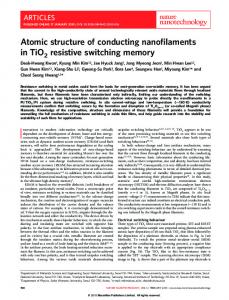
Fig. 1(a) shows X-ray diffraction (XRD) spectra in glancing 2θ scan mode of NiO thin films deposited in oxygen partial pressures of 5%–30%. The position of NiO diffraction peaks (111), (200), and (220) decreased with increasing oxygen contents, and the differences in peak position point to an increase in the lattice constant with higher oxygen content likely to be from increased strain effect due to increased nickel vacancies as oxygen content was raised. Fig. 1(b) shows the change in lattice constant calculated from Bragg’s law for the (111), (200), and (220) NiO peaks in the diffraction pattern of as-deposited samples from 5% to 20% oxygen partial pressure. The lattice
0741-3106/$26.00 © 2010 IEEE Authorized licensed use limited to: Samsung Electronics. Downloaded on June 26,2010 at 02:42:12 UTC from IEEE Xplore. Restrictions apply.
726
IEEE ELECTRON DEVICE LETTERS, VOL. 31, NO. 7, JULY 2010
Fig. 2. (a) Deposited at 5% oxygen partial pressure. (b) Deposited at 30% oxygen partial pressure. Samples deposited at 10%–30% oxygen partial pressure showed similar lack of metallic Ni peak.
Fig. 1. (a) XRD spectra of as-deposited NiO films prepared at 5%–30% oxygen partial pressure. (b) Change in lattice constant calculated from NiO (111), (200), and (220) peaks as oxygen partial pressure increases during deposition. (c) I–V curves of NiO films deposited at 5%–30% oxygen partial pressure. (d) Depth profile of oxygen and nickel composition by XPS for 30%–5%–30% NiO multilayer sample.
constants of films fabricated between 5% and 8%, calculated from XRD, are close to the lattice parameter of 0.4177 nm for bulk NiO [7]. With increasing lattice constant, the lattice parameter increases by about 0.83%, indicating a large amount of strain present in the films deposited at higher oxygen partial pressures. Additionally, as the shift in the (111), (200), and (220) planes is nearly equal, it indicates the presence of hydrostatic stresses within the film, rather than an in-plane or out-of-plane effect due to substrate lattice mismatch. The stresses are attributed to the effects of strain from a large number of metal vacancies spread homogenously throughout the film. Fig. 1(c) shows the current-versus-voltage (I–V ) characteristics of NiO films deposited at 5%–30% oxygen partial pressure. The leakage current increases as oxygen partial pressure increases, since higher oxygen partial pressure may induce both Ni vacancies and compensating holes inside a NiO film that shows intrinsically p-type semiconducting behaviors [4]. Meanwhile, we also observe some features in the XRD spectra that we point out here. First is that, for the samples deposited at 5% oxygen partial pressure, which are the only samples that show bistable resistance switching, there is a clear presence of Ni (111) peak, indicating that crystalline Ni is present. However, in the highresistance state, the conduction is dominated by the NiO matrix, even in the presence of metallic Ni content. Second, at 30%, the intensity of the NiO peak decreases abruptly, becoming nearly amorphouslike. Confirmation of graded oxygen content in our films was performed by XPS. Fig. 1(d) shows the depth profile of nickel and oxygen atomic content analysis of multilayer (5% switching and 30% envelope layer) NiO sample by XPS. The difference in each type of layer can be seen, as well as the diffusion at the interface. In order to investigate more details of the chemical states, depth profile XPS analysis on the surface and after 5, 10, and 15 min of sputtering was performed for the reference films deposited at each respective oxygen partial
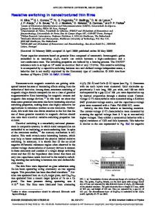
pressure of 5% and 30%, as shown in Fig. 2(a) and (b). The 5% sample shows a clear metallic Ni state peak at 862.7 eV, which the sample deposited at 30% oxygen partial pressure lacked. Both 5% and 30% layers showed the existence of NiO peaks, demonstrating that the 5% samples consist of coexisting Ni and NiO, indicating that bistable resistance switching may be related to metallic Ni contents in the switching layer [4]. Envelope layers with higher oxygen content, such as those deposited at 30% oxygen partial pressure, will naturally increase the envelope–switching interface layer thickness at each interface through oxygen diffusion compared to envelope layers deposited at lower oxygen partial pressures such as 10%. Reduction of the reset current value from ∼20 mA to ∼200 μA can be seen in Fig. 3(a) and (b). In addition, improved distribution in bistable resistance state and switching voltages was observed, as seen by comparison of Fig. 3(a) and (b), which are repeated switching measurements for single-layer (1-mA compliance current) and multilayer samples (200- μA compliance current), respectively. Because the single-layer sample has a broader distribution, it requires a larger compliance current to ensure switching for all cycles. Meanwhile, the current compliance within the submilliampere to few milliampere ranges did not affect the reset switching current. In a multilayer structure, the layers will be connected in serial resistance connections, and the lower resistivity of the 30% envelope layer is appropriate to act as a buffer during electrical switching. Fig. 3(c) shows the retention characteristics of multilayer samples. High- and low-resistance-state retention was almost constant over 100 h at 150 ◦ C. In addition, cells were seen to cycle more than 5 × 10² times in dc sweep measurement mode, as shown in Fig. 3(d). IV. D ISCUSSION Both reduction of switching current and improved distributions can be explained by envelope layers playing a role of buffer or diffused interface layer about the metallic switching filaments. The current in bistable resistance switching samples is localized near the grain boundaries; this is also shown in other works where the presence of metallic Ni is found near the grain boundaries as well [8]. As oxygen partial pressure is increased during deposition, the XRD and XPS data show that there is a reduction in active switching sites or grain boundaries. We believe that it is this phenomenon which can lead to the
Authorized licensed use limited to: Samsung Electronics. Downloaded on June 26,2010 at 02:42:12 UTC from IEEE Xplore. Restrictions apply.
LEE et al.: IMPROVED RESISTIVE SWITCHING RELIABILITY IN GRADED NiO MULTILAYER
727
V. C ONCLUSION In conclusion, we have fabricated a multilayer structure using higher oxygen content NiO to envelope the lower oxygen content NiO. The resulting sandwich structures showed lowered reset current values by nearly two orders of magnitude, and improved switching voltage and current distribution characteristics. We believe that the diffused regions are responsible in both cases, as shown by the relationship between reset current and envelope oxygen content. Also, as shown by XPS data, we confirm that metallic Ni coexists within a NiO matrix for active switching layers. Meanwhile, higher oxygen content layers were amorphouslike without any clear grain boundaries or metallic Ni content and did not exhibit bistable resistance switching. The improved switching behaviors through the use of NiO at different stoichiometries offer a new method for highdensity stacked-structure memory applications. R EFERENCES
Fig. 3. I–V switching characteristics of multi- and single-layer NiO films with top and bottom Pt metal electrodes. (a) Repeated switching characteristics of single-layer samples (50 nm thick). (b) Repeated switching characteristics of multilayer samples with envelope layers. (c) Retention characteristics of multilayer samples at 150 ◦ C. (d) Endurance properties of multilayer samples. (e) Schematic cross-sectional diagram showing how buffer layers are expected to improve electrical characteristics.
envelope layers acting as a buffer layer for switching. In the view that bistable resistance switching is caused by the formation and destruction of nanofilaments between the electrodes, successive measurements lead to a wider distribution in nanofilament sizes and composition in the single-layer sample. However, for NiO multilayer samples, the higher thermal conductivity Pt electrodes at 0.73 W/cm/◦ C compared to that of envelope NiO at 0.71 W/cm/◦ C can act to confine the thermal dissociation of nanofilaments, providing more control while also acting as oxygen containing a buffer layer, as described in other works [9], [10]. Also, the diffused interface layers decrease the actual active switching layer, which reduces the reset currents, as shown for smaller sized cells [5]. Also, as reported with IrO2 buffer layers [11], we believe that the oxygen containing envelope layers provides a similar effect in improving the distribution, but without using a different material, which is more advantageous. Although a more detailed study is required, the diagrams of the mechanisms that are believed to lead to improved characteristics are described in Fig. 3(e).
[1] M.-J. Lee, S. I. Kim, C. B. Lee, H. Yin, S.-E. Ahn, B. S. Kang, K. H. Kim, J. C. Park, C. J. Kim, I. Song, S. W. Kim, G. Stefanovich, J. H. Lee, S. J. Chung, Y. H. Kim, and Y. Park, “Low temperature grown transition metal oxide based storage materials and oxide transistor for high density nonvolatile memory,” Adv. Funct. Mater., vol. 19, no. 10, pp. 1587–1593, May 2009. [2] K. H. Kim, B. S. Kang, M.-J. Lee, S.-E. Ahn, C. B. Lee, G. Stefanovich, W. X. Xianyu, C. J. Kim, and Y. Park, “Multilevel programmable oxide diode for cross-point memory by electrical-pulse-induced resistance change,” IEEE Electron Device Lett., vol. 30, no. 10, pp. 1036–1038, Oct. 2009. [3] K. Szot, W. Speier, G. Bihlmayer, and R. Waser, “Switching the electrical resistance of individual dislocations in single-crystalline SrTiO3,” Nat. Mater., vol. 5, no. 4, pp. 312–320, Apr. 2006. [4] M.-J. Lee, S. Seo, D. C. Kim, S. E. Ahn, D. H. Seo, I. K. Yoo, I. G. Baek, D. S. Kim, I. S. Byun, S. H. Kim, I. R. Hwang, J. S. Kim, S. H. Jeon, and B. H. Park, “A low-temperature-grown oxide diode as a new switch element for high-density, nonvolatile memories,” Adv. Mater., vol. 19, no. 1, pp. 73–76, Jan. 2007. [5] S.-E. Ahn, B. S. Kang, K. H. Kim, M. J. Lee, C. B. Lee, G. Stefanovich, C. J. Kim, and Y. Park, “Stackable all oxide based nonvolatile memory with Al2O3 antifuse and p-CuOx/n-InZnOx diode,” IEEE Electron Device Lett., vol. 30, no. 5, pp. 550–552, May 2009. [6] I. G. Baek, D. C. Kim, M. J. Lee, H.-J. Kim, E. K. Yim, M. S. Lee, J. E. Lee, S. E. Ahn, S. Seo, J. H. Lee, J. C. Park, Y. K. Cha, S. O. Park, H. S. Kim, I. K. Yoo, U-I. Chung, J. T. Moon, and B. I. Ryu, “Multi-layer cross-point binary oxide resistive memory (OxRRAM) for post-NAND storage application,” in IEDM Tech. Dig., Dec. 2005, pp. 750–753. [7] Z. G. Yu, S. Krishnamurthy, and S. Guha, “Photoexcited-carrier-induced refractive index change in small bandgap semiconductors,” J. Opt. Soc. Amer. B, Opt. Phys., vol. 23, no. 11, pp. 2356–2360, Nov. 2006. [8] G.-S. Park, X.-S. Li, D.-C. Kim, R.-J. Jung, M.-J. Lee, and S. Seo, “Observation of electric-field induced Ni filament channels in polycrystalline NiOx films,” Appl. Phys. Lett., vol. 91, no. 22, p. 222 103, Nov. 2007. [9] Y. Sato, K. Kinoshita, M. Aoki, and Y. Sugiyama, “Consideration of switching mechanism of binary metal oxide resistive junctions using a thermal reaction model,” Appl. Phys. Lett., vol. 90, no. 3, p. 033 503, Jan. 2007. [10] M. J. Lee, S. Han, S. H. Jeon, B. H. Park, B. S. Kang, S.-E. Ahn, K. H. Kim, C. B. Lee, C. J. Kim, I.-K. Yoo, D. H. Seo, X.-S. Li, J.-B. Park, J.-H. Lee, and Y. Park, “Electrical manipulation of nanofilaments in transition-metal oxides for resistance-based memory,” Nano Lett., vol. 9, no. 4, pp. 1476–1481, Apr. 2009. [11] D. C. Kim, M. J. Lee, S. E. Ahn, S. Seo, J. C. Park, I. K. Yoo, I. G. Baek, H. J. Kim, E. K. Yim, J. E. Lee, S. O. Park, H. S. Kim, U.-I. Chung, J. T. Moon, and B. I. Ryu, “Improvement of resistive memory switching in NiO using IrO2 ,” Appl. Phys. Lett., vol. 88, no. 23, p. 232 106, Jun. 2006.
Authorized licensed use limited to: Samsung Electronics. Downloaded on June 26,2010 at 02:42:12 UTC from IEEE Xplore. Restrictions apply.