Sep 21, 2015 - Jalan Ganesha 10 Bandung, 40132, Indonesia ... of conventional two-level inverter in high power applications [1-4]. ... level inverter, the twenty five percent third harmonic signal (a sinusoidal signal with frequency ..... the injection signal takes its simplest form i.e the twenty five percent third harmonic only for.
International Journal on Electrical Engineering and Informatics - Volume 7, Number 3, September 2015
Influence of Third Harmonic Injection Signal on Output Current Ripple and Neutral Current of Three-Level PWM Inverter I Made Wiwit Kastawan1, Agung Harsoyo2, Mervin Tangguar Hutabarat2, and Pekik Argo Dahono2 1
Department of Energy Conversion Engineering, Politeknik Negeri Bandung, Jalan Ciwaruga, Bandung, Indonesia 2 School of Electrical Engineering and Informatics, Institute of Technology Bandung, Jalan Ganesha 10 Bandung, 40132, Indonesia Abstract: The influence of injecting third harmonic signal into three-phase sinusoidal reference signal of natural sampled PWM technique on output current ripple and neutral current of three-level inverter is analyzed in this paper. Expressions for both inverter output current ripple and neutral current as a function of PWM reference signal are derived first. Then, it is shown that injecting one fourth or twenty five percent third harmonic signal into three-phase sinusoidal reference signal may produce minimum output current ripple and neutral current. The twenty five percent third harmonic injection signal can simultaneously minimize output current ripple and neutral current of the three-level inverter only for unity power factor operation. Simulation and experimental results are included to show validity of the analysis results. Keywords: current ripple; neutral current; PWM technique; third harmonic; three-level inverter. 1. Introduction Multilevel inverter is a technology originally introduced to cope with problems due to use of conventional two-level inverter in high power applications [1-4]. Among many kinds of multilevel inverter structure, diode-clamped three-level inverter or shortly three-level inverter is the most accepted for industrial applications [4-6]. Using three-level inverter gives advantages such as produces lower output current ripple without necessarily using high switching frequency and applies lower voltage stress on inverter switches. However, threelevel inverter has a problem of neutral current flow which leads to unbalance neutral voltage. For many years, pulse width modulation (PWM) has been accepted as a standard technique to control inverter switching process [7-8]. Various PWM techniques have been developed, among them is the popular natural sampled PWM technique. Various methods to develop this natural sampled PWM technique, particularly the ones aimed to reduce or even minimize inverter output current ripple, were also proposed. Most popular one is the third harmonic injection method, in which the reference signal used is three-phase sinusoidal injected by third harmonic signal instead of three-phase sinusoidal signal only [9-11]. For conventional twolevel inverter, the twenty five percent third harmonic signal (a sinusoidal signal with frequency three times of reference signal frequency and amplitude one fourth or twenty five percent of reference signal amplitude) has been proven to be the optimum injection signal that results in minimum output current ripple and minimum input voltage ripple for unity power factor operation [11]. Regarding the neutral current or unbalance neutral voltage problem of threelevel inverter, many papers describing method to analyze and minimize it were published. Ogasawara et al studied the importance of zero sequence voltage on neutral current of threelevel inverter and expression of zero sequence voltage to reduce it has been derived. Unfortunately, use of zero sequence voltage makes the control more complicated [12]. Other papers provided analysis of unbalance neutral voltage based on space vector PWM (SVPWM) technique [13-16]. Basically all these methods have the same principle i.e. utilizing small redundant vectors in such a way to achieve balance neutral voltage. However, determination of Received: November 21st, 2014. Accepted: September 21st, 2015 DOI: 10.15676/ijeei.2015.7.3.1 366
I Made Wiwit Kastawan, et al.
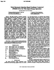
voltage reference vectors, sequence and duty cycle of active voltage vectors of the SVPWM technique are much more complicated. This paper presents analysis on the influence of injecting third harmonic signal into threephase sinusoidal reference signal of natural sampled PWM technique on output current ripple and neutral current of three-level inverters. It is shown that third harmonic injection signal can be used to minimize both output current ripple and neutral current of three-level PWM inverters. The twenty five percent third harmonic injection signal makes inverter output current ripple and neutral current simultaneously minimum only for unity power factor operation. In order to give systematic descriptions, the remaining of this paper will be organized as follows: Section 2 will describes in brief about three-level PWM inverter. In Section 3, the influence of third harmonic injection signal on output current ripple of three-level inverter is analyzed. Meanwhile, influence of third harmonic injection signal on neutral current of three-level inverter is going to be analyzed in Section 4. All analysis results are then verified by simulation and experimental results described in Section 5. Finally, the paper is concluded in Section 6. 2. Three-Level PWM Inverter Structure of the three-level inverter is shown in Figure 1. As shown by Table 1, this inverter has three switching states namely positive (Pos), zero (0) and negative (Neg) with the associated output phase voltage levels. These switching states are commonly realized by PWM technique, one example is the natural sampled PWM technique. Natural sampled PWM technique for three-level inverter requires two level-shifted triangular carrier signals, VT1 and VT2, with no phase difference between them. The reference signals are three-phase sinusoidal vu, vv, and vw. Figure 2 illustrates how intersections between reference and carrier signals produce the switching states and output phase voltages given in Table 1. il
id
Ld ic Cd
D1u Ed
Sv1
Sw1
Su2
Sv2
Sw2
D1w
u
N
Vd
Su1
D1v iU Three phase load iV
v
w iW
D1u’ Cd
Su3
Sv3
Sw3
D1v’ Ed
D1w’ Su4
Sv4
Sw4
Figure 1. Structure of three-level inverter Table 1. Switching states and output phase voltages of the three-level inverter. Switch state
No 1 2 3
Sx1 ON OFF OFF
Sx2 ON ON OFF
Sx3 OFF ON ON
Sx4 OFF OFF ON
Note: index x refers to phase u, v, or w.
367
Output phase voltage vxN Ed 0 –Ed
Remarks Positive (Pos) Zero (0) Negative (Neg)
VT1
vu
vw
vv
VT2
VT 0 -VT Ed
(a)
0 -Ed
(b)
Figure 2. (a) Reference and carrier signals of three-level PWM inverter (b) Output voltage for phase u. 3. Output Current Ripple of Three-Level PWM Inverter To investigate the influence of third harmonic injection signal on output current ripple of three-level PWM inverter, it is necessary to derive the expression for output current ripple first. Assumptions below are taken when deriving the expression: a) The input dc voltage, Ed, is ripple free and has a constant value. b) Carrier/switching frequency (fs) is much higher than reference frequency (fr). c) Dead time effect is negligible. d) Inverter load is balance three-phase load. Each phase load consists of a resistance (RL), an inductance (LL) and a sinusoidal back emf (e) connected in series. The reference signals are three-phase sinusoidal injected by arbritrary signal, s0, and expressed as: 𝑣𝑢 = 𝑘 sin(𝜃) + 𝑠0 ; 𝑣𝑣 = 𝑘 sin (𝜃 −
2𝜋 3
) + 𝑠0 ; and 𝑣𝑤 = 𝑘 sin (𝜃 +
2𝜋 3
) + 𝑠0
(1)
in which θ = 2πfrt and k is the modulation index i.e. a ratio between sinusoidal part of reference signal amplitude and the unity value of twice of carrier signal amplitude. To begin the analysis, half of the reference signal period is divided into thirty analysis intervals with thirty different switching states. Figure 3 shows the switching states/output voltages generated in an analysis interval. From this figure, relation between time parameters, carrier signals and reference signals can be easily derived as: 𝑡1 = (𝑇𝑆 ⁄2)𝑣𝑢 ; 𝑡2 = (𝑇𝑆 ⁄2)(1 + 𝑣𝑣 ); and 𝑡3 = (𝑇𝑆 ⁄2)𝑣𝑤 (2) The phase to phase voltage ripples are derived by applying principle of Fourier series expansion. For example, voltage ripple between phases u and v is derived as: ~
~
∞
~
𝑣𝑢𝑣 = 𝑣𝑢N − 𝑣𝑣N = ∑
(𝑎𝑛,𝑢 − 𝑎𝑛,𝑣 ) cos (
𝑛=1
2𝑛𝜋𝑡 𝑇𝑠
)
(3)
where: 𝑎𝑛,𝑢 = 𝑇𝑠⁄ 2
∫
𝑡2
2 𝑇𝑠
∫
𝑡1
−𝑡1
𝑣𝑢𝑁 (𝑡)cos (
𝑣𝑣𝑁 (𝑡)cos (
2𝑛𝜋𝑡 𝑇𝑠
2𝑛𝜋𝑡 𝑇𝑠
) ⅆ𝑡;
𝑎𝑛,𝑣 =
) ⅆ𝑡]
2 𝑇𝑠
[∫
−𝑡2
𝑇 − 𝑠⁄2
𝑣𝑣𝑁 (𝑡)cos (
2𝑛𝜋𝑡 𝑇𝑠
) ⅆ𝑡 + (4)
Then, current ripple for load between phases u and v in delta configuration is going to be: ~
∞
𝑖 𝑢𝑣 = ∑
~
𝑣𝑢𝑣
(5)
𝑛=1 𝑛 𝜔 𝐿𝐿
368
I Made Wiwit Kastawan, et al.
where ω = 2πfs. Due to high switching frequency, evaluation of (5) is sufficient for n = 1. Evaluating (3), (4), and (5) with substitution of (1) and (2) yields the load current ripple expression as follows: 𝐾 2𝜋 2𝜋𝑡 𝑖̃𝑢𝑣 = 12 [sin 𝜋(𝑘 sin 𝜃 + 𝑠0 ) + sin 𝜋 (𝑘 sin (𝜃 − ) + 𝑠0 )] cos ( ) (6) 𝜋
3
𝑇𝑆
𝐸 𝑇
with 𝐾1 = 𝑑 𝑆. The above analysis steps must be performed to the twenty nine analysis 𝐿 intervals remain. The result is a set of load current ripple expression given by Table 2. v VT Vw
Vu
0
Vv –VT Ed
0
VuN
0
VvN
–Ed Ed VwN
0
- Ts/2
- t3
- t2
- t1 0 t1
t2
t3
Ts/2
Figure 3. Output voltages generated in an analysis interval. Table 2. Load current ripple expressions. Interval 0≤𝜃≤ 𝜋 ≤𝜃 3 2𝜋 ≤ 3 2𝜋 ≤𝜃 3 ≤𝜋
𝜋 3
Equation 𝑖̃𝑢𝑣 =
𝐾1 2𝜋 2𝜋𝑡 [sin 𝜋(𝑘 sin 𝜃 + 𝑠0 ) + sin 𝜋 (𝑘 sin (𝜃 − ) + 𝑠0 )] cos ( ) 𝜋2 3 𝑇𝑆
𝑖̃𝑢𝑣 =
𝐾1 2𝜋 2𝜋𝑡 [sin 𝜋(𝑘 sin 𝜃 + 𝑠0 ) + sin 𝜋 (𝑘 sin (𝜃 − ) + 𝑠0 )] cos ( ) 2 𝜋 3 𝑇𝑆
𝑖̃𝑢𝑣 =
𝐾1 2𝜋 2𝜋𝑡 [sin 𝜋(𝑘 sin 𝜃 + 𝑠0 ) − sin 𝜋 (𝑘 sin (𝜃 − ) + 𝑠0 )] cos ( ) 2 𝜋 3 𝑇𝑆
Using expressions given by Table 2, the effective value of load/output current ripple of three-level PWM inverter will be obtained as follows: a) For s0 = 0 (no signal injected into reference signal)
369
b) 𝐼̃𝑢𝑣𝑆𝐼𝑁 =
1 √2𝜋5
(8.744𝑘 2 − 32.120𝑘 4 + 47.819𝑘 6 − 35.241𝑘 8 + 15.567𝑘10 − 4.603𝑘12 + 1
0.976𝑘14 − 0.152𝑘16 + 0.017𝑘18 )2 1 c) For s0 = 𝑘 sin[3𝜃] (injected by twenty five percent third harmonic) 4 1 d) 𝐼̃𝑢𝑣𝑆𝐼𝑁34 = (4.917𝑘 2 − 16.145𝑘 4 + 20.227𝑘 6 − 12.162𝑘 8 + 4.325𝑘10 − 5 √2𝜋
1
12
1.025𝑘 + 0.174𝑘14 − 0.022𝑘16 + 0.002𝑘18 )2 1 e) For s0 = 𝑘 sin[3𝜃] (injected by seventeen percent third harmonic) 6
f) 𝐼̃𝑢𝑣𝑆𝐼𝑁36 =
1 √2𝜋5
(7)
(8)
(5.619𝑘 2 − 17.997𝑘 4 + 21.774𝑘 6 − 12.572𝑘 8 + 4.271𝑘10 − 1
0.962𝑘12 + 0.155𝑘14 − 0.019𝑘16 + 0.002𝑘18 )2
(9)
Figure 4 shows the line plot of output current ripples expressed by (7) – (9). The figure shows clearly that third harmonic injection signal can be used to reduce output current ripple of three-level PWM inverter and minimum output current ripple is obtained by injecting twenty five percent third harmonic signal into three-phase sinusoidal reference signal. 𝐼̃ℎ𝑢𝑣 𝐾1 (A) uv
0.05
0.04
SIN SIN36 0.03
SIN34 0.02
0.01
k 0.2
0.4
0.6
0.8
1.0
Figure 4. Output current ripples of three-level PWM inverter. Using twenty five percent third harmonic injection signal to minimize output current ripple of three-level PWM inverter is confirmed by mathematical analysis. By taking the derivation of total mean square value of load current ripple to arbritrary injected signal, s0, which is followed by equalizing it to zero then expressions of injection signal given by Table 3 will be obtained. These expressions can be approximated as: 1 s0 = 𝑘 sin[3𝜃] (10) 4
which is the twenty five percent third harmonic injection signal. Table 3. Expressions of injection signal for minimizing output current ripple. Interval Equation 𝜋 1 0≤𝜃≤ s0 = (√3cos[𝜃] + sin[𝜃])𝑘 3 8 𝜋 2𝜋 1 ≤𝜃≤ s0 = − sin[𝜃]𝑘 3 3 4 2𝜋 1 ≤𝜃≤𝜋 s0 = (−√3cos[𝜃] + sin[𝜃])𝑘 3 8
370
I Made Wiwit Kastawan, et al.
4. Neutral Current of Three-Level PWM Inverter When zero switching state is achieved, the neutral point of three-level inverter (N) is connected to its output phase line allowing current to flow out-of or into neutral point, known as neutral current (IN), and causing unbalance neutral voltage. Therefor, neutral current of the condition shown previously in Figure 3 can be derived as: 𝐼𝑁 =
2 𝑇𝑆
𝑡
𝑡
𝑡
1
2
𝑇𝑆
(∫0 1(𝑖𝑣 ) 𝑑𝑡 + ∫𝑡 2(𝑖𝑢 + 𝑖𝑣 ) 𝑑𝑡 + ∫𝑡 3(𝑖𝑢 ) 𝑑𝑡 + ∫𝑡 2 (𝑖𝑢 + 𝑖𝑤 ) 𝑑𝑡 ) 3
(11)
If the inverter phase currents are defined as: 𝑖𝑢 = √2 𝐼𝑟𝑚𝑠 sin(𝜃 − ∅); 𝑖𝑣 = √2 𝐼𝑟𝑚𝑠 sin ((𝜃 − (2𝜋⁄3)) − ∅); and
𝑖𝑤 =
√2 𝐼𝑟𝑚𝑠 sin ((𝜃 + (2𝜋⁄3)) − ∅)
(12)
where ∅ is phase angle and cos(∅) is load power factor (pf), then evaluating (11) followed by substitution of (1), (2) and (12) results in: 𝐼𝑁 =
𝐼𝑟𝑚𝑠 (𝑘(cos[2𝜃−∅]−cos[∅]+√3sin[2𝜃−∅])−2(√3cos[𝜃−∅]+sin[𝜃−∅])𝑠𝑜 )
Interval 𝜋 0≤𝜃≤ 3 𝜋 2𝜋 ≤𝜃≤ 3 3 2𝜋 ≤𝜃≤𝜋 3 4𝜋 𝜋≤𝜃≤ 3 4𝜋 ≤𝜃 3 5𝜋 ≤ 3 5𝜋 ≤𝜃 3 ≤ 2𝜋
√2
(13)
Table 4. Neutral current expressions. Equation 𝐼𝑟𝑚𝑠 (𝑘(cos[2𝜃 − ∅] − cos[∅] + √3sin[2𝜃 − ∅]) − 2(√3cos[𝜃 − ∅] + sin[𝜃 − ∅])𝑠𝑜 )⁄√2
𝐼𝑟𝑚𝑠 (𝑘(2cos[2𝜃 − ∅] + cos[∅]) − 4sin[𝜃 − ∅]𝑠𝑜 )⁄√2 𝐼𝑟𝑚𝑠 (𝑘(cos[2𝜃 − ∅] − cos[∅] − √3sin[2𝜃 − ∅]) + 2(√3cos[𝜃 − ∅] − sin[𝜃 − ∅])𝑠𝑜 )⁄√2 𝐼𝑟𝑚𝑠 (𝑘(−cos[2𝜃 − ∅] + cos[∅] − √3sin[2𝜃 − ∅]) + 2(√3cos[𝜃 − ∅] + sin[𝜃 − ∅])𝑠𝑜 )⁄√2
−𝐼𝑟𝑚𝑠 (𝑘(2cos[2𝜃 − ∅] + cos[∅]) − 4sin[𝜃 − ∅]𝑠𝑜 )⁄√2
𝐼𝑟𝑚𝑠 (𝑘(−cos[2𝜃 − ∅] + cos[∅] + √3sin[2𝜃 − ∅]) + 2(−√3cos[𝜃 − ∅] + sin[𝜃 − ∅])𝑠𝑜 )⁄√2
In deriving neutral current of the three-level PWM inverter, analysis interval are identified along the reference period. Thus, a total of sixty analysis intervals are obtained. Table 4 gives the expressions of neutral current obtained after performing the above analysis steps to all sixty analysis intervals have been identified. If we take the derivation of mean square value of inverter neutral current to arbritrary injected signal, s0, followed by equalizing it to zero then expressions of injection signal given by Table 5 will be obtained. Figure 5 shows the line plot of the injection signal expressions. It can be seen that it is a third harmonic signal with waveform strongly affected by load pf. As shown by Figure 5 (a), the injection signal takes its simplest form i.e the twenty five percent third harmonic only for unity pf operation. This is also the injection signal that produces minimum output current ripple for three-level inverter (according to analysis results described previously in Section 3) as well as for conventional two-level inverter [11]. For load with pf lower than unity, Figure 5 (b) shows that injection signal turns into a more complex periodic discontinuous signal, although its frequency remains three times reference signal frequency. After performing several mathematical simplification process, this complicated signal can be approximated by a more simple expression as follows: 𝑘 𝑠0 ′ = ((4 cos ∅ sin 3𝜃) − (6 sin ∅ cos 3𝜃)) (14) 5𝜋
371
Table 5. Expressions of injection signal for minimizing neutral current Interval Equation
(0 − 𝜋⁄3); (𝜋 − 4𝜋⁄3) (𝜋⁄3 − 2𝜋⁄3); (4𝜋⁄3 − 5𝜋⁄3) (2𝜋⁄3 − 𝜋); (5𝜋⁄3 − 2𝜋)
1 𝑠0 = 𝑘((cos[2𝜃 − ∅] − cos[∅] + √3sin[2𝜃 − ∅])⁄(√3cos[𝜃 − ∅] + sin[𝜃 − ∅])) 2
1 𝑠0 = 𝑘((2cos[2𝜃 − ∅] + cos[∅])⁄sin[𝜃 − ∅]) 4 1 𝑠0 = 𝑘((−cos[2𝜃 − ∅] + cos[∅] + √3sin[2𝜃 − ∅])⁄(√3cos[𝜃 − ∅] − sin[𝜃 − ∅])) 2
Figure 5. Injection signal to minimize neutral current (a) pf = 1, (b) pf = 0.8. Using expressions given by Table 4, the effective value of neutral current of three-level PWM inverter can be obtained as: a) For s0 = 0 (no signal injected into reference signal) 𝐼𝑁𝑟𝑚𝑠𝑆𝐼𝑁 = 𝑘 𝐼𝑟𝑚𝑠 [ (
−3√3+𝜋 4𝜋
1
) cos[2∅] + (
−6√3+5𝜋 4𝜋
1 2
)]
(15)
b) For s0 = 𝑘 sin[3𝜃] (injected by twenty five percent third harmonic) 4
𝐼𝑁𝑟𝑚𝑠𝑆𝐼𝑁34 = 𝑘 𝐼𝑟𝑚𝑠 [ ( 1
3√3−32𝜋 128𝜋
) cos[2∅] + (
−264√3+176𝜋 128𝜋
1 2
)]
(16)
c) For s0 = 𝑘 sin[3𝜃] (injected by seventeen percent third harmonic) 6
𝐼𝑁𝑟𝑚𝑠𝑆𝐼𝑁36 = 𝑘 𝐼𝑟𝑚𝑠 [ (
−81√3−24𝜋
𝑘
288𝜋
) cos[2∅] + (
−540√3+376𝜋 288𝜋
1 2
)]
(17)
d) For s0 = ((4 cos ∅ sin 3𝜃) − (6 sin ∅ cos 3𝜃)) (injected by the approximated injection 5𝜋 signal) (
(
𝐼𝑁𝑟𝑚𝑠𝑆𝐼𝑁3′ = 𝑘 𝐼𝑟𝑚𝑠
+( [
−90√3𝜋−400𝜋2
) cos[∅] −
200𝜋3 160𝜋−594√3+150√3𝜋2 −50𝜋3 200𝜋3
90√3𝜋+80𝜋2 200𝜋3
+(
1 2
) 𝐶𝑜𝑠[3∅] − (
) cos[2∅]
189√3 200𝜋3
416𝜋+27√3−300√3𝜋2 +250𝜋3 200𝜋3
(18)
) cos[4∅] )
]
Figure 6 shows the line plot of inverter neutral currents expressed by (15) – (18). This figure confirms that third harmonic injection signal can be used to reduce and minimize neutral current of three-level PWM inverter. The twenty five percent third harmonic injection signal gives minimum neutral current of three-level PWM inverter only for unity pf operation.
372
I Made Wiwit Kastawan, et al.
Figure 6. Neutral current of three-level PWM inverter (a) pf = 0.85, (b) pf = 1. 5. Simulation and Experimental Results An experimental system shown by Figure 7 has been constructed to verify the analysis results. Power MOSFETs with high switching frequency are selected as the switches of threelevel inverter. The load is static balance three-phase load. The load impedance and switching frequency have to be carefully determine to assure that load time constant is higher than inverter switching period. Thus, 19.51 ohm per-phase resistance, 5.89 mH per-phase inductance and 1 kHz switching frequency have been selected. The reference frequency of the inverter is 50 Hz. A three-phase full-bridge rectifier is used to generate a 100 V dc voltage fed into the input terminal of three-level inverter. The PWM switching pulse is generated by FPGA modul. To get a more comprehensive comparison, simulations using a software commonly used to simulate electrical power circuit i.e. PSIM@ version 9.0.3 are performed. Figures 8 and 9 show comparison of simulation, experimental and analysis/calculated results for output current ripple and neutral current respectively. Both figures show that simulation results are very close to calculated results. Average errors between simulation and calculated results are about 3.9% and 5,7% for output current ripple and neutral current respectively. Although the average errors between experimental and calculated results are slightly higher i.e 10.4% and 12.3% for output current ripple and neutral current respectively, but the shape and pattern of curves depicted from experimental results are very similar to the curves depicted from calculated results. Experimental results emerge higher error because ideal conditions assumed for analysis are not completely fulfilled such as dead time that is not equal to zero and dc supply voltage that can not be maintained constant and ripple free. Thus, validity of the calculated/analysis results can be appreciated from these simulation and experimental results.
DC supply
+ -
Three-level inverter
Delta connected three-phase load
DC – AC
FPGA Figure 7. Block diagram of the three-level PWM inverter experimental system.
373
Figure 8. Calculated, simulation and experimental results of output current ripple of three-level PWM inverter.
Figure 9. Calculated, simulatioan and experimental results of neutral current of three-level PWM inverter. Table 6. Output current ripple of three-level PWM inverter k 0.0 0.1 0.2 0.3 0.4 0.5 0.6 0.7 0.8 0.9 1.0
SIN 0.0000 0.1992 0.3768 0.5134 0.5948 0.6147 0.5779 0.5085 0.4639 0.5213 0.6882
Calculated SIN36 0.0000 0.1601 0.3048 0.4203 0.4948 0.5204 0.4944 0.4216 0.3233 0.2683 0.3568
SIN34 0.0000 0.1497 0.2848 0.3917 0.4598 0.4818 0.4559 0.3887 0.3046 0.2736 0.3704
SIN 0.0000 0.2091 0.3666 0.5021 0.5886 0.6027 0.5532 0.5026 0.4745 0.5270 0.6747
374
Simulation SIN36 0.0000 0.1629 0.3124 0.4208 0.4903 0.5351 0.4951 0.4351 0.3162 0.2709 0.3606
SIN34 0.0000 0.1475 0.2806 0.3938 0.4749 0.4931 0.4527 0.3826 0.3040 0.2759 0.3675
SIN 0.0000 0.2291 0.3770 0.5189 0.5425 0.5543 0.4984 0.4424 0.4368 0.5169 0.6141
Experimental SIN36 0.0000 0.2025 0.3352 0.4234 0.4577 0.4852 0.4322 0.3325 0.2786 0.2660 0.3216
SIN34 0.0000 0.1948 0.3170 0.4132 0.4438 0.4766 0.4199 0.3173 0.2509 0.2802 0.3279
I Made Wiwit Kastawan, et al.
Note: 1. The unit for values in table is ampere (A) 2. SIN is without injection signal 3. SIN36 is with seventeen percent third harmonic injection signal 4. SIN34 is with twenty five percent third harmonic injection signal Table 7. Neutral current of three-level PWM inverter k 0 0.1 0.2 0.3 0.4 0.5 0.6 0.7 0.8 0.9 1 k 0 0.1 0.2 0.3 0.4 0.5 0.6 0.7 0.8 0.9 1
SIN 0.0000 0.0332 0.1326 0.2981 0.5297 0.8274 1.1916 1.6224 2.1203 2.6853 3.3179
Calculated SIN36 SIN34 0.0000 0.0000 0.0188 0.0168 0.0822 0.0735 0.1893 0.1692 0.3397 0.3037 0.5336 0.4768 0.7703 0.6882 1.0497 0.9377 1.3714 1.2250 1.7353 1.5498 2.1409 1.9117
SIN3’ 0.0000 0.0029 0.0091 0.0199 0.0354 0.0556 0.0805 0.1098 0.1437 0.1819 0.2257
SIN 0.0000 0.0410 0.1048 0.2219 0.4823 0.6350 1.0045 1.3838 1.8221 2.2446 2.6966
Experimental SIN36 SIN34 0.0000 0.0000 0.0337 0.0335 0.0263 0.0263 0.1023 0.0926 0.2489 0.2285 0.3676 0.3273 0.5670 0.5160 0.8115 0.7715 1.0910 0.8510 1.3280 1.0230 1.6670 1.2650
SIN3’ 0.0000 0.0196 0.0273 0.0395 0.0428 0.0612 0.1111 0.1339 0.1934 0.2349 0.3081
SIN 0.0000 0.0329 0.1321 0.2971 0.5277 0.8231 1.1862 1.6155 2.1090 2.6689 3.2967
Simulation SIN36 SIN34 0.0000 0.0000 0.0165 0.0141 0.0753 0.0066 0.1761 0.1545 0.3175 0.2800 0.5008 0.4403 0.7239 0.6351 0.9851 0.8632 1.2855 1.1258 1.6250 1.4215 1.9997 1.7511
SIN3’ 0.0000 0.0046 0.0149 0.0310 0.0525 0.0790 0.1083 0.1426 0.1773 0.2142 0.2552
Note: The unit for values in table is ampere (A) SIN is without injection signal SIN36 is with seventeen percent third harmonic injection signal SIN34 is with twenty five percent third harmonic injection signal SIN3’ is with approximated third harmonic injection signal
Table 6 and Table 7 show respectively values of output current ripple and neutral current of the three-level PWM inverter as modulation index varies from zero to unity (k = 0 – 1). It can be seen from both tables that injecting third harmonic signal into three-phase sinusoidal reference signal of the natural sampled PWM technique results in significant reduction of both output current ripple and neutral current of three-level inverter. According to Table 6, using seventeen percent third harmonic injection signal gives reduction of output ripple current in range of 14.4% - 48.5% or approximately 24,8% in average (based on calculated data), 10.5% 48.6% or approximately 23.3% in average (based on simulation data), and 11.1% - 48.5% or approximately 24.0% in average (based on experimental data). More significant output current ripple reduction is achieved when twenty five percent third harmonic injection signal used. It reduce the output current ripple of three-level PWM inverter in range of 21.1% - 47.5% or approximately 29,0% in average (based on calculated data), 18.2% - 47.6% or approximately 28.3% in average (based on simulation data), and 14.0% - 46.6% or approximately 26.2% in average (based on experimental data). Using twenty five percent third harmonic injection signal gives maximum reduction or minimum value of output current ripple of three-level PWM inverter. Further analysis shows that output current ripple reduction higher than 30% will be achieved if the modulation index is higher 0.7. According to Table 7, using seventeen percent third harmonic injection signal gives reduction of neutral current in range of 35.3% 43.4% or approximately 36,6% in average (based on calculated data), 39.0% - 49.8% or approximately 40.8% in average (based on simulation data), and 40.1% - 53.9% or approximately 43.6% in average (based on experimental data). Higher neutral current reduction is achieved when twenty five percent third harmonic signal is injected into three-phase
375
sinusoidal reference signal of the natural sampled PWM technique. Neutral current reduction is in range of 42.2% - 49.4% or approximately 43,4% in average (based on calculated data), 46.5% - 57.1% or approximately 48.0% in average (based on simulation data), and 44.2% 58.3% or approximately 51.6% in average (based on experimental data). The highest or maximum neutral current reduction will be achieved if the approximated third harmonic injection signal used. Ranges of neutral current reduction are 91.3% - 93.3% or approximately 93.0% (based on calculated data), 86.0% - 92.3% or approximately 90.3% in average (based on simulation data), and 82.2% - 91.1% or approximately 88.8% in average (based on experimental data). The reduction is very significant and the neutral current is minimum. The approximated third harmonic injection signal will become twenty five percent third harmonic signal if the inverter operates in unity pf. Data of neutral current reduction of three-level PWM inverter listed in Table 7 also show that modulation index has no effect. Percentage of neutral current reduction varies slightly when modulation index varies from zero to unity. 6. Conclusion The influence of third harmonic injection signal on output current ripple and neutral current of three-level PWM inverter has been analyzed. It is shown that third harmonic injection signal can be used to produce minimum output current ripple and neutral current. However, in general the third harmonic injection signal which produces minimum output current ripple is different from that which produces minimum neutral current. The twenty five percent third harmonic injection signal simultaneously produces minimum output current ripple and minimum neutral current only for unity power factor operation. 7. References [1]. D. G. Holmes and T. A. Lipo, “Pulse Width Modulation for Power Converters. Principles and Practice”, IEEE Press Series on Power Engineering, Wiley-Interscience, p. 38-55 , 2003 [2]. N. S. Choi, J. G. Cho, and G. H. Cho, “A General Circuit Topology of Multilevel Inverter”, IEEE/PESC, pp. 96-103, 1991. [3]. Menzies, P. Steimer, and J. K. Steinke, “Five Level GTO Inverters For Large Induction Motor Drives”, in IEEE/IAS Annual Meeting, pp. 595-601, 1993. [4]. J. Rodriguez, J. S. Lai, F. Z. Peng, “Multilevel Inverter: A Survey of Topologies, Controls and Applications”, IEEE Transactions on Industrial Electronics, 49 (4), pp. 724-738, 2002. [5]. H. P. Krug. T. Kume, M. Swamy, “Neutral -Point Clamped Three-Level General Purpose Inverter-Features, Benefits and Applications”, in 35th Annual IEEE Power Electronics Specialists Conference, pp. 323-328, 2004. [6]. R. Teichmann, S. Bernet, “A Comparison of Three-Level Converters versus Two-Level Converters for Low-Voltage Drives, Traction, and Utility Applications”, IEEE Transactions on Industry Applications, 41 (3), pp. 855-865, May/Jun 2005. [7]. J. Holtz, “Pulsewidth Modulation for Electronic Power Conversion”, Proceedings of the IEEE, 82 (8), pp. 1194-1214, Aug 1994. [8]. M. A. Patel, A. R. Patel, D. R. Vyas, K. M. Patel, “Use of PWM Techniques for Power Quality Improvement”, International Journal of Recent Trends in Engineering, 1 (4), pp. 99-102, May 2009. [9]. J. A. Houldsworth, D. A. Grant, “The Use of Harmonic Distortion to Increase the Output Voltage of a Three-Phase PWM Inverter”, IEEE Transcations on Industry Applications, IA-20 (5), pp. 1224-1228, Sep/Oct 1984. [10]. M. A. Boost, P. D. Ziogas, “State of The Art Carrier PWM Techniques: A Critical Evaluation”, IEEE Transactions on Industry Applications, 24 (2), pp. 271-280, Mar/Apr 1988.
376
I Made Wiwit Kastawan, et al.
[11]. P. A. Dahono, Y. Sato, T. Kataoka, “Analysis and Minimization of Harmonics in The AC and DC Sides of PWM Inverters”, IEE Japan Transactions on Industry Applications, pp. 553-561, May 1995. [12]. S. Ogasawara, H. Akagi, “Analysis of Variation of Neutral Point Potential in NeutralPoint-Clamped Voltage Source PWM Inverters”, in Conf. Rec. IEEE-IAS Annual Meeting, pp. 965-970, 1993. [13]. D. H. Lee, S.R. Lee, F. C. Lee, “An Analysis of Midpoint Balance for The Neutral Point Clamped Three-Level VSI”, IEEE Annual Power Electronics Specialists Conference, pp. 193-199, 1998. [14]. K. Shinohara, E. Sakasegawa, “A New PWM Method With Suppressed Neutral Point Potential Variation of Three-Level Inverter for AC Servo Motor Drive”, IEEE International Conference on PEDS, pp. 668-672, 1999. [15]. K. Yamanaka, A. M. Hava, H. Kirino,Y. Tanaka, N. Koga, T. Kume, “A Novel Neutral Poin Potential Stabilization Technique Using the Information of Output Current Polarities and Voltage Vector”, IEEE Transactions on Industry Applications, Vol. 38, No. 6, pp. 1572-1580, Nov/Dec 2002. [16]. J. Zaragoza, J. Pou, S. Ceballos, M. Saeedifard, D. Boroyevich, “A Carrier Based PWM Strategy With Zero-Sequence Voltage Injection for A Three-Level NPC Converter”, IEEE Transactions on Power Electronics, Vol. 27, No. 2, Feb 2012.
I Made Wiwit Kastawan was born in Denpasar, Indonesia in 1974. He received the B.Eng. and M.Eng. degrees in electrical engineering from Institute of Technology Bandung (ITB), Indonesia, in 1998 and 2002, respectively. He also received M.Sc. degree in energy engineering from Royal Institute of Technology (KTH), Stockkholm, Sweden in 2002. He received Doctor degree in electrical engineering from ITB, Indonesia, in 2013. He was a researcher at Electrical Energy Conversion Research Laboratory, School of Electrical Engineering and Informatics (STEI), ITB, during 1999 – 2003. Since 2004 he joined the Department of Energy Conversion Engineering, State Polytechnic of Bandung (Polban), Indonesia, as a lecturer. He has research interests in power converter and harmonics elimination techniques and actively publish papers in the related area in some national and international conferences.
Agung Harsoyo was born in Yogyakarta, Indonesia, in 1969. He received B.Eng. degree in telecommunication engineering from Institute of Technology Bandung (ITB), Indonesia, in 1993. He received M.Sc degree in optoelectronics and M.Eng degree in signal processing on telecommunication both in 1996 from Université de Bretagne Occidentale (UBO), France and Université de Bretagne Sud (UBS), France respectively. In 2003, he received Doctor degree in optical and electromagnetic also from Université de Bretagne Sud (UBS), France. His fields of research include electromagnetic system, signal processing, telecommunication network and information system and technology. Dr. Agung Harsoyo is the recipient of ICT Award (Ina-Icta) for two consecutive years, in 2009 and 2010. He has long experience of research and profesional work in area related to his expertise since 1994. Dr. Agung Harsoyo was appointed to be the head of Control System and Computer Laboratory, School of Electrical Engineering and Informatics (STEI), ITB, in 2004. He is at STEI, ITB, since 1993.
377
Mervin Tangguar Hutabarat (member of IEEE) received the Engineer degree in Electrical Engineering from Institute of Technology Bandung (ITB), Indonesia in 1988, M.Sc. degree in Electrical Engineering from the Ohio State University (OSU), Columbus OH, USA in 1992 and PhD. degree in Electronics from University College London (UCL), London, UK in 2000. His current research interests include linear and nonlinear devices and circuits.
Pekik Argo Dahono received the Engineer degree from the Institute of Technology Bandung, Indonesia, the Master and Doctor of Engineering degrees from Tokyo Institute of Technology, Japan, in 1985, 1992 and 1995, respectively, all in electrical engineering. He is a Senior Member of the Institute of Electrical and Electronic Engineers. His fields of research are power electronics and electrical machinery. He is a recipient of the PII Engineering Award and also ASEAN Outstanding Engineering Achievement award both in 2006. He has published more than 100 papers in international conferences and journals. He has received several best paper awards. He is registered as Insinyur Profesional Utama and ASEAN Chartered Professional Engineer. At present, he is an associate professor in the School of Electrical Engineering and Informatics, Institute of Technology Bandung, Indonesia.
378